On-demand quantum storage of photonic qubits in an on-chip waveguide
Abstract
Photonic quantum memory is the core element in quantum information processing (QIP). For the scalable and convenient practical applications, great efforts have been devoted to the integrated quantum memory based on various waveguides fabricated in solids. However, on-demand storage of qubits, which is an essential requirement for QIP, is still challenging to be implemented using such integrated quantum memory. Here we report the on-demand storage of time-bin qubits in an on-chip waveguide memory fabricated on the surface of a 151Eu3+:Y2SiO5 crystal, utilizing the Stark-modulated atomic frequency comb protocol. A qubit storage fidelity of is obtained with single-photon-level coherent pulses, far beyond the highest fidelity achievable using the classical measure-and-prepare strategy. The developed integrated quantum memory with the on-demand retrieval capability represents an important step toward practical applications of integrated quantum nodes in quantum networks.
Photonic quantum memory plays an important role in quantum information processing (QIP). Typical applications include enabling the long-distance quantum communication based on the quantum repeater approach [1, 2, 3], enhancing the precision of quantum metrology [4, 5], converting the heralded photons to on-demand photons [6] and synchronizing the operations in quantum computation [7, 2]. Quantum memory based on the integrated structure can further meet the requirements of ease of use, robustness and low consumption for scalable networking applications [8]. Photonic storage has been successfully implemented in the integrated quantum memory based on various fabrication methods applied in rare-earth-ion (REI) -doped solids, such as femtosecond-laser micromachining (FLM) [9, 10, 11, 12, 13], focused-ion-beam milled nanoresonators [14, 15, 16, 17] and lithium niobate waveguides [8, 18, 19, 20].
As a synchronizing tool in QIP, on-demand readout of photonic qubits is a fundamental requirement for quantum memory [1, 2]. A typical solution, as widely employed in bulk material, is reversibly transferring the optical collective excitation into the spin-wave excitation using strong control pulses [21, 22, 23, 24]. However, filtering of such strong control pulses in the integrated waveguide structure is extremely challenging due to the overlapped spatial mode between single photons and control pulses. As a result, to date, the demonstrated integrated quantum storage based on REI-doped solids is limited to a preprogrammed delay, mostly based on the atomic frequency comb (AFC) protocol [10, 11, 14, 17, 8, 18, 19]. The only exception is the recent demonstration in a nanophotonic resonator fabricated in a : crystal, in which a dynamically controlled shift of AFC delay up to 10 ns is obtained [14]. Unfortunately, the controlled shift is less than the duration of the readout pulse, which severely limits its practical applications.
Here we report the high-fidelity and on-demand storage of time-bin qubits in an integrated quantum memory with a controlled storage time exceeding 2 s, far beyond the pulse width (100 ns). The recently proposed Stark-modulated AFC protocol [25] is implemented in a FLM on-chip waveguide to achieve the goal of noise-free on-demand photonic qubit storage. This protocol is further modified here to introduce two electric pulses with opposite directions to eliminate the dephasing caused by the unwanted inhomogeneity in Stark shifts [26].
The AFC scheme has been one of the most successful protocols implemented in REI-doped solids with the advantages of wideband operation [8, 27], large multimode capacity [11, 19, 28], and high fidelity [29, 30]. The basic idea of this scheme is to prepare an absorption profile with a comb structure in the inhomogeneously broadened optical transition. An input photon will be absorbed by the AFC and the natural atomic dephasing will lead to a collective echo emission at the predetermined time of due to the periodical absorption structure, where is the periodicity of the comb [29, 21].
Originated in [31], the electric field gradient has been introduced to AFC protocol aiming at on-demand readout in discrete steps. Recently, Horvath et al. [25] proposed a Stark-modulated AFC protocol, in which two homogeneous electric field pulses are employed for storage time control, and a high signal-to-noise ratio (SNR) storage is demonstrated in a : crystal. Since no strong control optical pulses are required here, this scheme is suitable for implementations in the integrated quantum memory.
For the crystal, when the electric field is applied along the crystallographic axis or in the mirror plane, the Stark effect splits two group ions that acquire frequency shifts of the same magnitudes but opposite directions [32, 25]. The magnitude of the frequency shift is , where is the difference between the ground state electric-dipole moment and the excited state electric-dipole moment , is the applied electric field, is the Planck constant.
Two groups of ions acquire the phases of and , respectively, for an electric field duration of . Considering the scenario when , the two groups of ions will accumulate a relative phase of , inducing a destructive interference, thus the original AFC echo at is effectively suppressed by the first electric pulse [25]. A second electric pulse applied at time window cancels the relative phase and leads to the on-demand retrieval of the echo at where is an integer and . The storage efficiency is [21, 25]:
| (1) |
where is the effective absorption depth of the comb and is the full width at half maximum (FWHM) of the single absorption peak.
In practice, the absorption peaks in the prepared AFC can be significantly broadened when the electric field is not homogeneous, this is the case in our experiments, as shown later. This electrically induced broadening causes an extra dephasing process during the total pulse duration () of two pulses. A similar mechanism has been discussed in Ref. [33]. In our case, this broadening already leads to strongly suppressed signal as compared to that expected from Eq. (1). Inspired by previous works [34, 33], here we apply the second electric field pulse with the same magnitude but the opposite direction with respect to the first pulse.
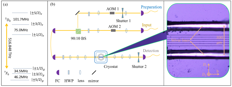
The experimental sample is a : crystal with an isotope enrichment of for 151Eu. The substrate crystal has a dimension of mm3 along the crystal’s axes and a dopant concentration of . A series of type IV waveguides are fabricated on the surface of the crystal utilizing the FLM system [13]. Compared to our previous result presented in Ref. [13], now we find better fabricating parameters. The 1030 nm femtosecond laser has a pulse duration of 210 fs and a repetition rate of 201.9 kHz. A objective (NA=0.65) is utilized to focus the laser beam. Here we choose the low pulse energy of 60 nJ and adopt the multiscan method [35, 36] to minimize the propagation loss in the waveguide. The chosen waveguide has an end-to-end device efficiency of , as defined by the ratio between the output of the single-mode fiber (SMF) and the input before the cryostat. This high device efficiency sets a new record for integrated photonic memories based on REI-doped solids. The waveguide mode is close to the Gaussian mode and has a FWHM of m [26]. As a comparison, the typical coupling efficiency is in the lithium niobate waveguide memory (waveguide mode size of m FWHM) [19, 8, 20, 37], while the coupling efficiency from the SMF to the focused-ion-beam milled waveguide memory is less than (fundamental mode volume of ) [38, 14] .
To introduce the required electric field for storage time control, two silver lines with a diameter of m and a spacing of m are buried in two grooves beside the waveguides (as shown in Fig. 1) which can apply electric field parallel to the axis. The grooves have a depth of approximately m and a width of about m, and are also fabricated with the FLM system.
The experimental setup for quantum storage is similar to that presented in our previous work [12]. The laser source is a frequency-doubled semiconductor laser which is externally locked at the frequency of 516.848 THz with a linewidth of subkilohertz. A cryostat (Montana Instrument) with a base temperature of 3.2 K is employed to cool down the sample. All optical pulses are modulated by the acoustic optic modulators (AOMs) which are driven by an arbitrary waveform generator. In addition, two mechanical shutters are placed in the pump path and before the single-photon detector (SPD), respectively, to protect the SPD in the preparation procedures. An arbitrary function generator (Tektronix, AFG3102C) is utilized to directly generate the electric pulses.
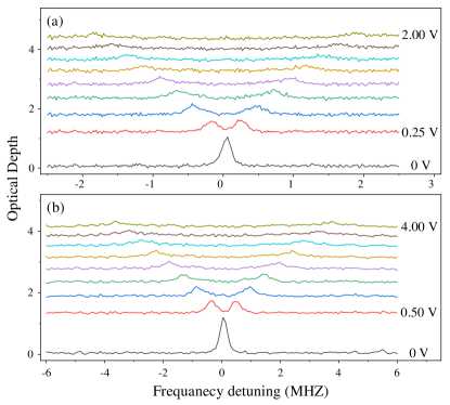
We characterize the Stark effect of our sample using spectral-hole burning measurements. We create a single absorption peak in the center of a transparent spectral window. The Stark coefficient can be obtained by looking on the frequency shift of the absorption peak in a dc bias electric field. Figure. 2(b) shows the linear shift of the peak when increasing the magnitude of the electric field. A linear fitting of the peak position of each peak gives a Stark coefficient of kHz/Vcm-1. Here, we do not pick up a single class of ions, i.e. various transitions between the hyperfine levels in the excited state and the ground state are involved [39]. Then we conduct the spectral-hole burning measurements again, while first isolating a single class of ions using the pumping scheme described in Ref. [12]. In this way, we specifically measure the Stark coefficient for the transition . The measured Stark coefficient is 28.6 kHz/Vcm-1 (Fig. 2(a)) which is basically the same as that obtained in Fig. 2(b), considering the errors in identifying the peak centers of the broadened peaks. Our measurement agrees with the value reported in the previous work [40].
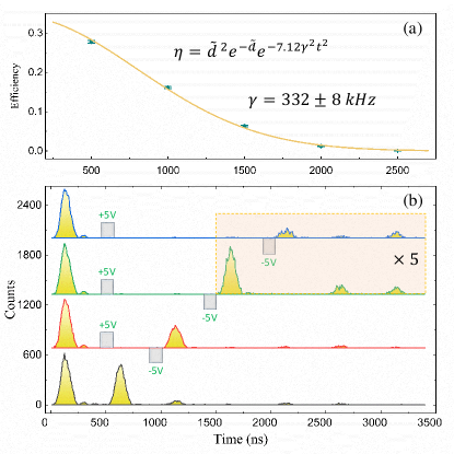
In order to increase the available optical depth for efficient storage, we pump the ions with transition frequency of (-72, -7) and (+7, +72) MHz, forming a strong absorption peak at with a bandwidth of 14 MHz and an optical depth of 5.9. An AFC with a total bandwidth of 11 MHz and a comb periodicity of MHz is prepared. On-demand retrieval of the AFC echo is enabled by applying two electric pulses with opposite directions as explained above. The electric pulse has a FWHM of 55 ns to induce a relative phase shift of between the two groups of ions to suppress the ordinary AFC echo. Fig. 3(b) presents the photon counting histograms of the on-demand AFC storage with a variable storage time up to 2 s, with an input of weak coherent pulse with the average photon number . The input signal pulse has a FWHM of 100 ns. The efficiency for a storage time of 1 s is , while a SNR of is obtained [26]. The storage efficiency as a function of the storage time (as shown in Fig. 3(a)) is well fitted by Eq. (1) with kHz and , demonstrating the dephasing caused by the inhomogeneity of Stark shifts is completely eliminated.
| Input state | |||||
|---|---|---|---|---|---|
| Fidelity |
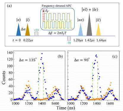
The above results demonstrate high-SNR storage of single-photon-level coherent states in the integrated memory and this device is ready for the qubit storage. Here we choose the time-bin encoded qubits which are particularly robust for long-distance transmission in optical fibers [41, 42]. The analysis of time-bin qubits requires an unbalanced Mach-Zehnder interferometer (MZI) for projection on a superposition basis [29, 23]. Here we rely on two superimposed AFC to serve as a built-in unbalanced MZI [29] and a dynamical phase is introduced by the frequency-detuned AFC [43] for projection on arbitrary superposition states [26].
The double AFC are programmed to give standard AFC storage times of 600 ns and 710 ns, respectively. Two single-photon-level coherent Gaussian pulses with a FWHM of 100 ns and a spacing of ns serve as input, generating a time-bin qubit with the form [23, 29], where and denote the early and late time bin, respectively. is the relative phase between two pulses and . As shown in Fig. 4(a), the memory outputs three time bins {}, after applying the second electric pulse.
The characterization of the is accomplished by introducing a certain amount of frequency detuning of the AFC featuring delay of 1/= 600 ns. The phase introduced by the detuned AFC is with a storage time of [43].
The fidelity for and is defined as , while is the noise and is the signal without including the noise [23]. The fidelity of and is measured to be and . We calculate the average fidelity as . The fidelity of the coherence measurement is defined as [44]. By varying the measurement phase through the frequency-detuned AFC, we measure the interference visibility for input states of and , as shown in Fig. 4. The interference visibility is , with and corresponding to the maximum and minimum photon counts measured with and , respectively. The storage fidelity for and is and , respectively, and the mean fidelity .
The total storage fidelity, as defined by [23] is calculated to be . As a comparison, one can calculate the best achievable fidelity using the classical measure-and-prepare strategy, taking into account the Poissonian statistics of the input and the finite storage efficiency [45, 24]. Considering the average photon number of 0.5 and the storage efficiency of in double AFC measurements, the strict classical fidelity bound is . The experimentally achieved fidelity violates the classical bound by more than 89 standard deviations, demonstrating its high reliability in qubit storage.
In conclusion, based on an on-chip waveguide memory combined with on-chip electrodes, we demonstrate on-demand storage of photonic time-bin qubits with the fidelity of . This is approximately the same as the highest fidelity obtained in a quantum memory based on the bulk material [30]. The small volume of the integrated memory enables the use of a transistor-transistor-logic-compatible voltage for actively controlling the storage time. In the current demonstration, the storage time is limited by the broadened absorption peaks. The storage time can be greatly extended with much narrower AFC peaks and is fundamentally limited by the optical coherence time [26]. This compact, reliable and low-insertion-loss integrated quantum memory shall enable plentiful applications in QIP, especially in the construction of large-scale quantum networks based on integrated quantum nodes.
Acknowledgments Chao Liu and Tian-Xiang Zhu contributed equally to this work. This work is supported by the National Key R&D Program of China (Grant No. 2017YFA0304100), the National Natural Science Foundation of China (Grant No. 11774331, No. 11774335, No. 11504362, No. 11821404, and No. 11654002), the Anhui Initiative in Quantum Information Technologies (Grant No. AHY020100), the Key Research Program of Frontier Sciences, the CAS (Grant No. QYZDY-SSW-SLH003), the Science Foundation of the CAS (Grant No. ZDRW-XH-2019-1) and the Fundamental Research Funds for the Central Universities (Grant No. WK2470000026, and No. WK2470000029). Z.-Q.Z acknowledges the support from the Youth Innovation Promotion Association CAS.
References
- Sangouard et al. [2011] N. Sangouard, C. Simon, H. De Riedmatten, and N. Gisin, Rev. Mod. Phys 83, 33 (2011).
- Lvovsky et al. [2009] A. I. Lvovsky, B. C. Sanders, and W. Tittel, Nat. photonics 3, 706 (2009).
- Duan et al. [2001] L.-M. Duan, M. D. Lukin, J. I. Cirac, and P. Zoller, Nature 414, 413 (2001).
- Gottesman et al. [2012] D. Gottesman, T. Jennewein, and S. Croke, Phys. Rev. Lett. 109, 070503 (2012).
- Komar et al. [2014] P. Komar, E. M. Kessler, M. Bishof, L. Jiang, A. S. Sørensen, J. Ye, and M. D. Lukin, Nat. Phys. 10, 582 (2014).
- Nunn et al. [2013] J. Nunn, N. Langford, W. Kolthammer, T. Champion, M. Sprague, P. Michelberger, X.-M. Jin, D. England, and I. Walmsley, Phys. Rev. Lett. 110, 133601 (2013).
- Knill et al. [2001] E. Knill, R. Laflamme, and G. J. Milburn, Nature 409, 46 (2001).
- Saglamyurek et al. [2011] E. Saglamyurek, N. Sinclair, J. Jin, J. A. Slater, D. Oblak, F. Bussieres, M. George, R. Ricken, W. Sohler, and W. Tittel, Nature 469, 512 (2011).
- Corrielli et al. [2016] G. Corrielli, A. Seri, M. Mazzera, R. Osellame, and H. De Riedmatten, Phys. Rev. Appl. 5, 054013 (2016).
- Seri et al. [2018] A. Seri, G. Corrielli, D. Lago-Rivera, A. Lenhard, H. de Riedmatten, R. Osellame, and M. Mazzera, Optica 5, 934 (2018).
- Seri et al. [2019] A. Seri, D. Lago-Rivera, A. Lenhard, G. Corrielli, R. Osellame, M. Mazzera, and H. de Riedmatten, Phys. Rev. Lett. 123, 080502 (2019).
- Liu et al. [2020] C. Liu, Z.-Q. Zhou, T.-X. Zhu, L. Zheng, M. Jin, X. Liu, P.-Y. Li, J.-Y. Huang, Y. Ma, T. Tu, et al., Optica 7, 192 (2020).
- Zhu et al. [2020] T.-X. Zhu, C. Liu, L. Zheng, Z.-Q. Zhou, C.-F. Li, and G.-C. Guo, Phys. Rev. Appl. 14, 054071 (2020).
- Zhong et al. [2017a] T. Zhong, J. M. Kindem, J. G. Bartholomew, J. Rochman, I. Craiciu, E. Miyazono, M. Bettinelli, E. Cavalli, V. Verma, S. W. Nam, et al., Science 357, 1392 (2017a).
- Zhong et al. [2015a] T. Zhong, J. M. Kindem, E. Miyazono, and A. Faraon, Nat. Commun. 6, 8206 (2015a).
- Zhong et al. [2017b] T. Zhong, J. M. Kindem, J. Rochman, and A. Faraon, Nat. Commun. 8, 14107 (2017b).
- Craiciu et al. [2019] I. Craiciu, M. Lei, J. Rochman, J. M. Kindem, J. G. Bartholomew, E. Miyazono, T. Zhong, N. Sinclair, and A. Faraon, Phys. Rev. Appl. 12, 024062 (2019).
- Sinclair et al. [2016] N. Sinclair, K. Heshami, C. Deshmukh, D. Oblak, C. Simon, and W. Tittel, Nat. Commun. 7, 13454 (2016).
- Sinclair et al. [2014] N. Sinclair, E. Saglamyurek, H. Mallahzadeh, J. A. Slater, M. George, R. Ricken, M. P. Hedges, D. Oblak, C. Simon, W. Sohler, et al., Phys. Rev. Lett. 113, 053603 (2014).
- Askarani et al. [2019] M. F. Askarani, M. G. Puigibert, T. Lutz, V. B. Verma, M. D. Shaw, S. W. Nam, N. Sinclair, D. Oblak, and W. Tittel, Phys. Rev. Appl. 11, 054056 (2019).
- Afzelius et al. [2009] M. Afzelius, C. Simon, H. De Riedmatten, and N. Gisin, Phys. Rev. A 79, 052329 (2009).
- Jobez et al. [2015] P. Jobez, C. Laplane, N. Timoney, N. Gisin, A. Ferrier, P. Goldner, and M. Afzelius, Phys. Rev. Lett. 114, 230502 (2015).
- Gündoğan et al. [2015] M. Gündoğan, P. M. Ledingham, K. Kutluer, M. Mazzera, and H. De Riedmatten, Phys. Rev. Lett. 114, 230501 (2015).
- Yang et al. [2018] T.-S. Yang, Z.-Q. Zhou, Y.-L. Hua, X. Liu, Z.-F. Li, P.-Y. Li, Y. Ma, C. Liu, P.-J. Liang, X. Li, et al., Nat. Commun. 9, 3407 (2018).
- Horvath et al. [2020] S. P. Horvath, M. K. Alqedra, A. Kinos, A. Walther, S. Kröll, and L. Rippe, arXiv preprint arXiv:2006.00943 (2020).
- [26] See supplemental material at [url will be inserted by publisher] for details about the protocol and experiments, which includes refs. [46, 47].
- Saglamyurek et al. [2016] E. Saglamyurek, M. G. Puigibert, Q. Zhou, L. Giner, F. Marsili, V. B. Verma, S. W. Nam, L. Oesterling, D. Nippa, D. Oblak, et al., Nat. Commun. 7, 11202 (2016).
- Zhou et al. [2015a] Z.-Q. Zhou, Y.-L. Hua, X. Liu, G. Chen, J.-S. Xu, Y.-J. Han, C.-F. Li, and G.-C. Guo, Phys. Rev. Lett. 115, 070502 (2015a).
- De Riedmatten et al. [2008] H. De Riedmatten, M. Afzelius, M. U. Staudt, C. Simon, and N. Gisin, Nature 456, 773 (2008).
- Zhou et al. [2012] Z.-Q. Zhou, W.-B. Lin, M. Yang, C.-F. Li, and G.-C. Guo, Phys. Rev. Lett. 108, 190505 (2012).
- Lauritzen et al. [2011] B. Lauritzen, J. Minář, H. De Riedmatten, M. Afzelius, and N. Gisin, Phys. Rev. A 83, 012318 (2011).
- Meixner et al. [1992] A. Meixner, C. Jefferson, and R. Macfarlane, Phys. Rev. B 46, 5912 (1992).
- Arcangeli et al. [2016] A. Arcangeli, A. Ferrier, and P. Goldner, Phys. Rev. A 93, 062303 (2016).
- Hedges et al. [2010] M. P. Hedges, J. J. Longdell, Y. Li, and M. J. Sellars, Nature 465, 1052 (2010).
- Osellame et al. [2007] R. Osellame, M. Lobino, N. Chiodo, M. Marangoni, G. Cerullo, R. Ramponi, H. Bookey, R. Thomson, N. Psaila, and A. Kar, Appl. Phys. Lett. 90, 241107 (2007).
- Rodenas and Kar [2011] A. Rodenas and A. K. Kar, Opt. Express 19, 17820 (2011).
- Staudt et al. [2007] M. U. Staudt, S. R. Hastings-Simon, M. Nilsson, M. Afzelius, V. Scarani, R. Ricken, H. Suche, W. Sohler, W. Tittel, and N. Gisin, Phys. Rev. Lett. 98, 113601 (2007).
- Zhong et al. [2016] T. Zhong, J. Rochman, J. M. Kindem, E. Miyazono, and A. Faraon, Opt. Express 24, 536 (2016).
- Lauritzen et al. [2012] B. Lauritzen, N. Timoney, N. Gisin, M. Afzelius, H. de Riedmatten, Y. Sun, R. Macfarlane, and R. Cone, Phys. Rev. B 85, 115111 (2012).
- Macfarlane et al. [2014] R. M. Macfarlane, A. Arcangeli, A. Ferrier, and P. Goldner, Phys. Rev. Lett. 113, 157603 (2014).
- Brendel et al. [1999] J. Brendel, N. Gisin, W. Tittel, and H. Zbinden, Phys. Rev. Lett. 82, 2594 (1999).
- Marcikic et al. [2002] I. Marcikic, H. de Riedmatten, W. Tittel, V. Scarani, H. Zbinden, and N. Gisin, Phys. Rev. A 66, 062308 (2002).
- Zhou et al. [2015b] Z.-Q. Zhou, S. F. Huelga, C.-F. Li, and G.-C. Guo, Phys. Rev. Lett. 115, 113002 (2015b).
- Marcikic et al. [2003] I. Marcikic, H. Riedmatten, W. Tittel, H. Zbinden, and N. Gisin, Nature 421, 509 (2003).
- Specht et al. [2011] H. Specht, C. Nölleke, A. Reiserer, M. Uphoff, E. Figueroa, S. Ritter, and G. Rempe, Nature 473, 190 (2011).
- Equall et al. [1994] R. W. Equall, Y. Sun, R. L. Cone, and R. M. Macfarlane, Phys. Rev. Lett. 72, 2179 (1994).
- Zhong et al. [2015b] M. Zhong, M. P. Hedges, R. L. Ahlefeldt, J. G. Bartholomew, S. E. Beavan, S. M. Wittig, J. J. Longdell, and M. J. Sellars, Nature 517, 177 (2015b).