Additional excitonic features and momentum-dark states in ReS2
Abstract
Unidirectional in-plane structural anisotropy in Rhenium-based dichalcogenides introduces a new class of 2-D materials, exhibiting anisotropic optical properties. In this work, we perform temperature dependent, polarization-resolved photoluminescence and reflectance measurements on several-layer ReS2. We discover two additional excitonic resonances (X3 and X4), which can be attributed to splitting of spin degenerate states. Strong in-plane oscillator strength of exciton species X1 and X2 are accompanied by weaker counterparts X3 and X4 with similar polarization orientations. The in-plane anisotropic dielectric function has been obtained for ReS2 which is essential for engineering light matter coupling for polarization sensitive optoelectronic devices. Furthermore, our temperature dependent study revealed the existence of low-lying momentum-forbidden dark states causing an anomalous PL intensity variation at 30 K, which has been elucidated using a rate equation model involving phonon scattering from these states. Our findings of the additional excitonic features and the momentum-dark states can shed light on the true nature of the electronic band structure of ReS2.
I Introduction
In-plane structural anisotropy in individual layers of van der Waals materials produces electronic bandstructures that are unique in contrast to the family of Transition Metal Dichalcogenides (TMDCs) with in-plane rotational symmetry. Rhenium (Re) based Group VII TMDCs like ReS2 have garnered considerable attention because of their intriguing anisotropic optical, vibrational and electronic properties arising from reduced crystal symmetry [1, 2, 3, 4, 5, 6, 7, 8, 9, 10, 11, 12, 13, 14]. This originates from ReS2’s distorted 1T structure [15], where the extra electron from the Re atom contributes to the strong Re-Re metal bond, forming a zigzag chain along the b-axis. This results in higher electron mobility along the b-axis [9], and optical anisotropy manifesting itself as highly polarized photoluminescence (PL) and absorption due to two strongly bound exciton species X1 and X2 with dipole moments along different in-plane directions [1, 5, 6, 7]. These properties open the door to a class of polarization-sensitive, on-chip devices like polarization controlled all-optical switches [16], polarized LEDs [17], photodetectors [18] and polarization-based quantum logic gates [19]. Additionally, for Group VI TMDCs the electronic and optical properties are strongly dependent on the number of layers of the crystal, and show a drastic change in the monolayer limit [20]. Conversely, ReS2 with its weak interlayer coupling shows no such drastic change when going from bulk to monolayer [2], making it ideal for multilayer photonic device applications. In order to create highly sensitive devices, however, a meticulous study of its anisotropic dielectric properties is required. Furthermore, there has been considerable debate about the nature of ReS2’s bandgap, with the recent consensus being that it is marginally indirect except in bilayer form [6, 8, 12, 21, 22]. Experimental studies that can shed light into this matter are essential.
In this work, we focus on high-resolution, polarization-resolved reflectance and PL at low temperature, discovering two additional exciton peaks that were predicted for ReS2 [4] but not observed in previous studies. It is envisaged that these two shoulder peaks denoted by X3 and X4 are observed due to the splitting of spin degenerate excitonic states by combined effect of electron-hole exchange interaction, structural anisotropy, and spin-orbit coupling. X3 and X4 appear on the higher energy sides in both the absorption and PL measurements with similar polarization orientation as X1 and X2 respectively. The anisotropic nature of ReS2’s dielectric properties is further demonstrated via polarization dependent reflectance. Transfer matrix method was utilized to understand the asymmetric excitonic lineshape in our reflectance from the ReS2/SiO2/Si dielectric stack as a function of layer thickness and thus extract the real and imaginary part of anisotropic refractive index of the material. In addition, we report excitation polarization dependence of the PL, which provides insight into the anisotropic absorption of this material. For excitation energy 1.88 eV, the integrated PL intensity from all four exciton species is maximized when excitation polarization is oriented along X2. Furthermore, our temperature-dependent study finds the four exciton peak positions are well resolved up to a temperature of 150 K, and their dipole orientations are preserved. Most intriguingly, we observe an anomalous PL intensity variation around 30 K, which necessitated the development of a model using rate equations, considering phonon scattering from low-lying dark exciton states. Our model provides evidence of the existence of indirect exciton states which are closely-lying below the bright excitons, confirming the quasi-indirect nature of ReS2’s bandgap. Our analysis can shed light on the understanding of the excitonic properties in this anisotropic material and provide useful information for photonics and optoelectronic device engineering with ReS2.
II Results and Discussion
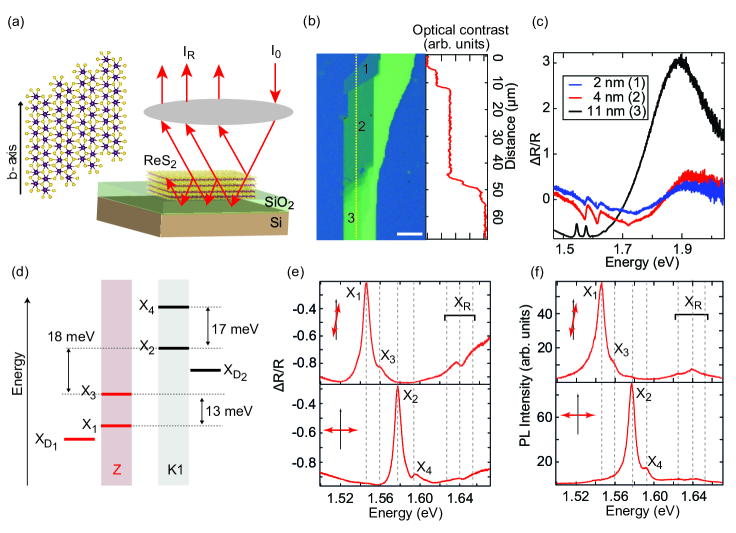
A schematic top view is shown in Fig. 1(a) of a single layer of ReS2, where each molecular layer is a sandwich of a Re layer between two S layers. The direction of the b-axis is marked by a solid arrow which can be identified from the optical image during measurement. Sample was prepared by mechanical exfoliation technique, and dry transferred on to 340 nm SiO2/Si substrate. The optical image of the sample is shown in Fig. 1(b) where we can approximately identify the number of layers from the optical contrast along a line profile, which has been further verified using AFM (see Fig. S1 in the Supplemental Material [23]). On-chip crystallographic orientation can be estimated by observing the sample edges, utilizing the fact that ReS2 is likely to cleave along the axis containing the covalent Re-S bonds, which is parallel to the b axis [1, 24].
Reflectance measurement was performed using a broadband halogen source with a spot size of 3 µm at three different points of the sample as shown in Fig. 1(b): Points 1, 2 and 3, being 2 nm, 4 nm and 11 nm thick respectively. At 11 nm thickness (point 3), ReS2 approaches its bulk character, wherein PL intensity becomes independent of the number of layers [1, 2]. However, its 2D character is preserved since excitons are confined mostly in single layers [3].
Excitonic features in PL and reflectivity are too broad at room temperature to resolve all the peaks, therefore, the sample was cooled down to 3.2 K in a closed cycle cryostat. The reflectivity measured at point 1 and 2 show an asymmetric lineshape about the excitonic resonance, as shown in Fig. 1(c). We see a pronounced red shift of exciton peak positions from few layers to bulk limit in agreement with previous reports [1, 5, 6]. In reflectivity data, we plot the differential reflectance, that is, , where and are the reflectance spectra from the sample and the SiO2/Si substrate respectively. Due to interference in the multilayer film system consisting of Si, SiO2 and ReS2 as shown in the schematic in Fig. 1(a), a broad anti-reflection dip coincides with the excitonic resonances. This makes the 11 nm ReS2 (at point 3) ideal to probe well-resolved exciton peaks in reflectance, which almost mimics the PL spectrum. Chosen thickness of the SiO2 layer and the dielectric properties of 11 nm ReS2 make these peaks show a background free, almost symmetric Fano lineshape. In contrast, the reflectivity measured at point 1 and 2 show asymmetric Fano lineshape, which is a result of interference with the background reflectivity with a relative phase change of across the exciton resonance [25]. The Fano asymmetry parameter varies across the three points. The peaks at higher energy range are the higher-order Rydberg series of the excitons [1, 5]. What follows below are based on experimental results conducted on the 11 nm ReS2.
We observe four peaks at 1.5450.001 (X1), 1.5580.001 (X3), 1.5760.001 (X2) and 1.5930.001 (X4) eV. The peaks at higher energy range are the higher-order Rydberg series of the excitons, denoted by X2 [1, 5]. The newly observed peaks X3 and X4 are in contrast to what has been observed earlier in ReSe2 [3], since they appear at the higher energy side of X1 and X2 respectively. However, from the resemblance between these additional peaks and the similar peaks for ReSe2, we speculate their origin is the splitting of singlet and triplet states of excitons due to electron-hole exchange interaction. Other plausible contributions for such splitting are the broken rotational symmetry due to structural anisotropy and spin-orbit coupling in ReS2. As shown in Fig. 1(d), we attribute the higher energy prominent exciton transition X2 to the K1 point, and X1 to the Z point of the Brillouin Zone, using the results of a recent, comprehensive ab-initio calculation [8]. XD1 and XD2 are low-lying momentum-dark states nearly degenerate with X1 and X2 respectively. They will be of interest when considering temperature dependence of PL intensity later in this paper. Figures 1(e) and 1(f) show the polarization resolved differential reflectance and PL at a polarization angle of -10∘ (top panels) and 90∘ (bottom panels) respectively, where all exciton peaks as seen in the reflectivity are also observed in PL with same energy positions. The 2 meV Stokes shift between PL emission and absorption peak (Fig. S2 in the Supplemental Material [23]) and the strong PL intensity indicates the pristine quality of our sample. We see no change in its optical properties over time and over multiple cooling cycles (Fig. S3 [23]).
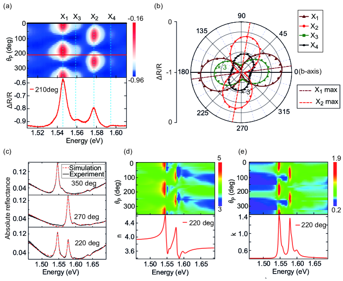
In the polarization resolved reflectance measurement, linearly polarized white light was used as the source and the reflected light was collected via 0.7 NA objective lens, while the excitation polarization angle is varied with respect to (w.r.t.) the b-axis using a half-wave plate. The experimental result for 11 nm ReS2 is shown in the colour plot in Fig. 2(a). A line plot in the bottom panel is chosen at an angle where we see all the four exciton resonances. The polar plot Fig. 2(b) shows that the two exciton species X1 and X2 are polarized at angles of 6∘ and 79∘ respectively w.r.t the b-axis (For fitting function see Supplemental Material [23]), which agrees with earlier reported values within experimental error [1, 8, 26]. X3 and X4 follow the polarization variation of X1 and X2 respectively.
As shown in Fig. 1(a), we model the polarization resolved reflectance via transfer matrix technique [27, 28, 29, 30, 31] (see Supplemental Material [23]) to obtain the reflectance spectrum of the ReS2/SiO2/Si stack and hence extract the frequency dependent dielectric function of ReS2. We fit the polarization-resolved reflectance to obtain the dielectric function for every polarization. The dielectric function is given by , where , , and are the background dielectric constant, oscillator strength, resonance frequency and the linewidth of the ith oscillator, and the summation is over all exciton resonances. Fig. 2(c) shows absolute reflectance spectra obtained at three different polarization angles of the linearly polarized incident beam, along with their theoretical fits. All the fitted parameters are given in Tables S1-S4 in Supplemental Material [23].
The anisotropic refractive index , where, and are the real and imaginary parts of refractive index, are shown in the colour plots Figs. 2(d) and 2(e) respectively. Interestingly, as shown in Fig. 2(c), we observed that the transfer matrix model best fit our experimental data with the polarization resolved reflectance only. However, in the Supplemental Material (Fig. S4 [23]) we show that it is not possible to obtain a good fit for unpolarized reflectance data with this model. As the unpolarized reflectance is a result of averaging over all polarization, it cannot be fitted by an effective value of the dielectric constant, since it is in truth highly anisotropic.
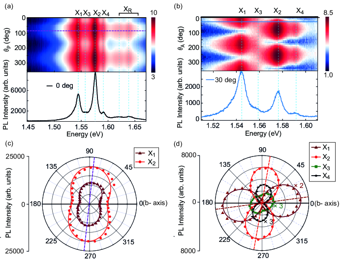
A 660 nm laser with a spot size of 1 µm is used to excite the sample with variable polarization w.r.t the b-axis. At first, the integrated PL was collected directly at the spectrometer slit without any analyzer at the output port. We discover that the overall PL intensity varies with the excitation polarization direction as shown in the colour plot in Fig. 3(a). The intensity of the overall spectrum is modulated; however, the intensity ratio of X1 and X2 remains unchanged as the incident polarization is varied. Intensity from all exciton species is maximum at a particular polarization of excitation laser, corresponding to an in-plane direction which turns out to be the polarization direction of the X2 exciton, within experimental error. This is a consequence of absorption at excitation energy 1.88 eV also being anisotropic, peaking at the angle along X2. This can be predicted from the angle dependent absorption obtained from our fitting (Fig. S5 [23]), and agrees with theoretical calculations [4]. The incident polarization dependence for two other lower excitation energies (1.76 and 1.70 eV) closer to X2 resonance was also tested, which showed slightly different behavior (Fig. S6 [23]). The anisotropy becomes more pronounced as the excitation energy comes closer to the exciton resonances.
Next, we keep the excitation polarization fixed at an angle for which the overall PL is maximum and measure the polarization state of the PL via an analyzer placed before the spectrometer slit. Data shown in Fig. 3(b) was recorded while rotating the analyzer angle from 0∘ to 360∘, where zero is along the b-axis. From the polar plot in Fig. 3(d), we find the two dominant emission peaks at X1 and X2 are polarized w.r.t the b-axis at angles of 6∘ and 82∘ respectively, which is same as the angles obtained from reflectance considering experimental error. It is observed as shown in Figs. 2(b) and 3(d) that the two shoulder peaks at X3 and X4 follow the same polarization directions as X1 and X2 respectively.
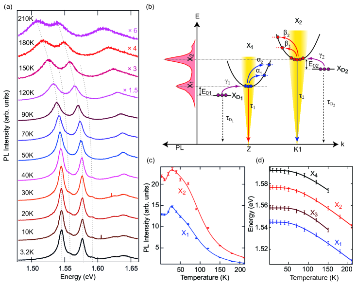
We perform a temperature-dependent PL measurement, the results of which are plotted in Fig. 4(a). The analyzer is fixed throughout at an angle for which all four exciton peaks are visible. The two shoulder peaks X3 and X4 are not resolvable above 150 K since they are dominated by X1 and X2 whose linewidths increase with temperature. We observe an anomalous temperature variation of PL intensity as shown in Fig. 4(c), with a maxima in intensity near 30K, which can be attributed to the presence of low-lying dark states (XD1, XD2). Spin-forbidden dark excitons [32] have recently been reported to be the cause of anomalous temperature dependent PL in Group VI TMDCs [33]. On the other hand, momentum-forbidden low-lying states have been hypothesized before to explain the ratio of X1 and X2 populations not following the expected Boltzmann distribution [1, 6]. This is also evident in Fig. 3 where it is observed that the X1 PL intensity is lower than X2 which is persistent even at higher temperatures as shown in Fig. 4(c). Time-resolved measurements have also revealed that the radiative lifetimes of excitons to be less than 10 ps [12], indicating the excitons are not thermalized.
To gain a comprehensive understanding of the temperature variation of this hot photoluminescence, we propose a rate equation model involving the bright (X1, X2) and dark states (XD1, XD2) as shown in the schematic diagram Fig. 4(b), where excitons in these states are generated via continuous wave (CW) pumping. Two kinds of phonon scattering are important in this model which are discussed below. First, scattering of excitons from XD1 to X1 and XD2 to X2 with rates and respectively, where and are the energy of the phonons involved. Second, , and , are the scattering rates from X1 and X2 to momentum-forbidden dark states outside the light cone. Excitons scatter to a continuum of states outside the light cone via phonons of all available energies. To simplify the model, we have considered only two different phonon energies per exciton state - , for X1 and , for X2. This effectively accounts for the scattering at both low temperature and high temperature regimes (see Fig. S10 in the Supplemental Material [23]).
We assume and are the radiative recombination times from X1 and X2, and and are the non-radiative recombination times from XD1 and XD2. By solving the rate equation under CW excitation (see Supplemental Material [23]), the PL intensity for X1 and X2 is obtained as a function of temperature, and fitted with the experimental data as shown in Fig. 4(c). From this model we find the two momentum-dark states XD1 and XD2 are present 16 meV and 5 meV below X1 and X2 states respectively. These dark states strongly indicate a quasi-indirect band gap at Z and K1 point in the Brillouin zone. This is in agreement with ab-initio calculations which indicate ReS2 is marginally indirect [6, 8].
When temperature is initially increased (3.2 KT30 K) X1 and X2 are thermally populated from XD1 and XD2 states by absorbing phonons. At the same time, X1 and X2 excitons are scattered from the radiative window to outside the light cone, where they recombine non-radiatively, by absorbing phonons of energy 17 meV and 3.2 meV respectively. In this temperature regime, we observe dark states are appreciably more populated than bright states on laser excitation, which results in a net gain in excitons scattered to the bright states. This causes PL intensity to increase to a maximum at 30K. At higher temperatures, the scattering process is mainly dominated by phonons of energies 52 meV and 41 meV from X1 and X2 states respectively. Scattering to dark states increases more rapidly than that to bright states after 30 K, causing PL intensity to decrease. All phonon energies obtained, except for 5 and 3.2 meV, have recently been reported for ReS2 [34]. From our fitting we also notice that the effective scattering time from X1 and X2 is much more than their recombination times, even up to high temperatures, which corroborates the fact that X1 and X2 emit hot photoluminescence.
We plot the observed redshift of exciton peak positions with temperature, and fit with the model describing the temperature dependence of a semiconductor bandgap [35]: . Here is the exciton resonance energy at T = 0 K, S is a dimensionless electron-phonon coupling constant, and is the average phonon energy. The fitted parameters are , and . The values of are 1.74, 1.78, 2.42 and 1.83 for X1, X2, X3 and X4 respectively, and is around 203 meV, concurring with earlier reports [36, 37]. Energy separation between the four exciton peaks remains constant with temperature as can be seen in Fig. 4(d). The angle between the excitons’ dipole moment orientation and b-axis remains unchanged with temperature indicates the temperature independent anisotropy (Fig. S7 [23]). Finally, temperature dependent reflectance measurements were used to acquire the corresponding dielectric function using the transfer matrix method (Fig. S8 [23]). shows significant change only near the exciton resonances.
III Conclusion
In conclusion, we observed two additional exciton shoulder peaks at higher energy sides of X1 and X2 which are attributed to splitting of spin degenerate exciton states. The ab initio calculations required to systematically investigate the exact origin of this splitting is beyond the scope of this work, and may be carried out in future studies. The transfer matrix method is utilized to extract the in-plane anisotropic complex dielectric function of several-layer ReS2 in unprecedented detail, which is crucial for modelling photonic devices or further experiments that make use of its anisotropic optical properties. Our temperature dependent study reveals an anomalous temperature variation in the PL intensity which underpins the existence of low-lying dark states, indicating quasi-indirect band gap in this system. The proposed mechanism considering the dynamical processes not only explains the observed temperature variation but also estimates the phonon energies supported by previous reports. It also establishes temperature dependent study as an accessible method to probe the existence of low-lying optically dark states.
Acknowledgements.
We acknowledge Dr. D. K. Goswami and his group for the AFM measurement on the sample. S. D. acknowledges SERB Ramanujan Fellowship, ISIRD grant, IIT Kharagpur and MHRD for the funding and support for this work. D. C. acknowledges CSIR for the financial assistance. We thank Dr. C. Chakraborty, and Dr. P. K. Chakraborty for their valuable comments on this work.References
- Aslan et al. [2016] O. B. Aslan, D. A. Chenet, A. M. van der Zande, J. C. Hone, and T. F. Heinz, Linearly Polarized Excitons in Single- and Few-Layer ReS 2 Crystals, ACS Photonics 3, 96 (2016).
- Tongay et al. [2014] S. Tongay, H. Sahin, C. Ko, A. Luce, W. Fan, K. Liu, J. Zhou, Y.-S. Huang, C.-H. Ho, J. Yan, D. F. Ogletree, S. Aloni, J. Ji, S. Li, J. Li, F. M. Peeters, and J. Wu, Monolayer behaviour in bulk ReS2 due to electronic and vibrational decoupling, Nat Commun 5, 3252 (2014).
- Arora et al. [2017] A. Arora, J. Noky, M. Drüppel, B. Jariwala, T. Deilmann, R. Schneider, R. Schmidt, O. Del Pozo-Zamudio, T. Stiehm, A. Bhattacharya, P. Krüger, S. Michaelis de Vasconcellos, M. Rohlfing, and R. Bratschitsch, Highly Anisotropic in-Plane Excitons in Atomically Thin and Bulklike 1 T ′-ReSe 2, Nano Lett. 17, 3202 (2017).
- Echeverry and Gerber [2018] J. P. Echeverry and I. C. Gerber, Theoretical investigations of the anisotropic optical properties of distorted 1 T ReS 2 and ReSe 2 monolayers, bilayers, and in the bulk limit, Phys. Rev. B 97, 075123 (2018).
- Jadczak et al. [2019] J. Jadczak, J. Kutrowska-Girzycka, T. Smoleński, P. Kossacki, Y. S. Huang, and L. Bryja, Exciton binding energy and hydrogenic Rydberg series in layered ReS2, Sci Rep 9, 1578 (2019).
- Urban et al. [2018] J. M. Urban, M. Baranowski, A. Kuc, Ł. Kłopotowski, A. Surrente, Y. Ma, D. Włodarczyk, A. Suchocki, D. Ovchinnikov, T. Heine, D. K. Maude, A. Kis, and P. Plochocka, Non equilibrium anisotropic excitons in atomically thin ReS 2, 2D Mater. 6, 015012 (2018).
- Sim et al. [2018] S. Sim, D. Lee, A. V. Trifonov, T. Kim, S. Cha, J. H. Sung, S. Cho, W. Shim, M.-H. Jo, and H. Choi, Ultrafast quantum beats of anisotropic excitons in atomically thin ReS2, Nat Commun 9, 351 (2018).
- Oliva et al. [2019] R. Oliva, M. Laurien, F. Dybala, J. Kopaczek, Y. Qin, S. Tongay, O. Rubel, and R. Kudrawiec, Pressure dependence of direct optical transitions in ReS2 and ReSe2, npj 2D Mater Appl 3, 20 (2019).
- Liu et al. [2015] E. Liu, Y. Fu, Y. Wang, Y. Feng, H. Liu, X. Wan, W. Zhou, B. Wang, L. Shao, C.-H. Ho, Y.-S. Huang, Z. Cao, L. Wang, A. Li, J. Zeng, F. Song, X. Wang, Y. Shi, H. Yuan, H. Y. Hwang, Y. Cui, F. Miao, and D. Xing, Integrated digital inverters based on two-dimensional anisotropic ReS2 field-effect transistors, Nat Commun 6, 6991 (2015).
- Cui et al. [2015] Q. Cui, J. He, M. Z. Bellus, M. Mirzokarimov, T. Hofmann, H.-Y. Chiu, M. Antonik, D. He, Y. Wang, and H. Zhao, Transient Absorption Measurements on Anisotropic Monolayer ReS 2, Small 11, 5565 (2015).
- Zhou et al. [2020] Y. Zhou, N. Maity, A. Rai, R. Juneja, X. Meng, A. Roy, Y. Zhang, X. Xu, J.-F. Lin, S. K. Banerjee, A. K. Singh, and Y. Wang, Stacking-Order-Driven Optical Properties and Carrier Dynamics in ReS 2, Adv. Mater. 32, 1908311 (2020).
- Wang et al. [2019] X. Wang, K. Shinokita, H. E. Lim, N. B. Mohamed, Y. Miyauchi, N. T. Cuong, S. Okada, and K. Matsuda, Direct and Indirect Exciton Dynamics in Few-Layered ReS 2 Revealed by Photoluminescence and Pump-Probe Spectroscopy, Adv. Funct. Mater. 29, 1806169 (2019).
- Sim et al. [2016] S. Sim, D. Lee, M. Noh, S. Cha, C. H. Soh, J. H. Sung, M.-H. Jo, and H. Choi, Selectively tunable optical Stark effect of anisotropic excitons in atomically thin ReS2, Nat Commun 7, 13569 (2016).
- Hafeez et al. [2017] M. Hafeez, L. Gan, A. Saleem Bhatti, and T. Zhai, Rhenium dichalcogenides (ReX 2 , X = S or Se): An emerging class of TMDs family, Mater. Chem. Front. 1, 1917 (2017).
- Wilson and Yoffe [1969] J. Wilson and A. Yoffe, The transition metal dichalcogenides discussion and interpretation of the observed optical, electrical and structural properties, Advances in Physics 18, 193 (1969).
- Sim et al. [2019] S. Sim, D. Lee, J. Lee, H. Bae, M. Noh, S. Cha, M.-H. Jo, K. Lee, and H. Choi, Light Polarization-Controlled Conversion of Ultrafast Coherent–Incoherent Exciton Dynamics in Few-Layer ReS 2, Nano Lett. 19, 7464 (2019).
- Wang et al. [2020] J. Wang, Y. J. Zhou, D. Xiang, S. J. Ng, K. Watanabe, T. Taniguchi, and G. Eda, Polarized Light-Emitting Diodes Based on Anisotropic Excitons in Few-Layer ReS 2, Adv. Mater. , 2001890 (2020).
- Zhang et al. [2015a] E. Zhang, Y. Jin, X. Yuan, W. Wang, C. Zhang, L. Tang, S. Liu, P. Zhou, W. Hu, and F. Xiu, ReS2-Based Field-Effect Transistors and Photodetectors, Adv. Funct. Mater. 25, 4076 (2015a).
- Kwon et al. [2019] J. Kwon, Y. Shin, H. Kwon, J. Y. Lee, H. Park, K. Watanabe, T. Taniguchi, J. Kim, C.-H. Lee, S. Im, and G.-H. Lee, All-2D ReS2 transistors with split gates for logic circuitry, Sci Rep 9, 10354 (2019).
- Splendiani et al. [2010] A. Splendiani, L. Sun, Y. Zhang, T. Li, J. Kim, C.-Y. Chim, G. Galli, and F. Wang, Emerging Photoluminescence in Monolayer MoS 2, Nano Lett. 10, 1271 (2010).
- Biswas et al. [2017] D. Biswas, A. M. Ganose, R. Yano, J. M. Riley, L. Bawden, O. J. Clark, J. Feng, L. Collins-Mcintyre, M. T. Sajjad, W. Meevasana, T. K. Kim, M. Hoesch, J. E. Rault, T. Sasagawa, D. O. Scanlon, and P. D. C. King, Narrow-band anisotropic electronic structure of ReS 2, Phys. Rev. B 96, 085205 (2017).
- Webb et al. [2017] J. L. Webb, L. S. Hart, D. Wolverson, C. Chen, J. Avila, and M. C. Asensio, Electronic band structure of ReS 2 by high-resolution angle-resolved photoemission spectroscopy, Phys. Rev. B 96, 115205 (2017).
- [23] See Supplemental Material for additional data and modeling, .
- Liang et al. [2009] C. Liang, Y. Chan, K. Tiong, Y. Huang, Y. Chen, D. Dumcenco, and C. Ho, Optical anisotropy of Au-doped ReS2 crystals, Journal of Alloys and Compounds 480, 94 (2009).
- Limonov et al. [2017] M. F. Limonov, M. V. Rybin, A. N. Poddubny, and Y. S. Kivshar, Fano resonances in photonics, Nature Photon 11, 543 (2017).
- Ho and Liu [2019] C.-H. Ho and Z.-Z. Liu, Complete-series excitonic dipole emissions in few layer ReS2 and ReSe2 observed by polarized photoluminescence spectroscopy, Nano Energy 56, 641 (2019).
- Blake et al. [2007] P. Blake, E. W. Hill, A. H. Castro Neto, K. S. Novoselov, D. Jiang, R. Yang, T. J. Booth, and A. K. Geim, Making graphene visible, Appl. Phys. Lett. 91, 063124 (2007).
- Li et al. [2014] Y. Li, A. Chernikov, X. Zhang, A. Rigosi, H. M. Hill, A. M. van der Zande, D. A. Chenet, E.-M. Shih, J. Hone, and T. F. Heinz, Measurement of the optical dielectric function of monolayer transition-metal dichalcogenides: MoS 2 , Mo S e 2 , WS 2 , and WS e 2, Phys. Rev. B 90, 205422 (2014).
- Zhang et al. [2015b] H. Zhang, Y. Ma, Y. Wan, X. Rong, Z. Xie, W. Wang, and L. Dai, Measuring the Refractive Index of Highly Crystalline Monolayer MoS2 with High Confidence, Sci Rep 5, 8440 (2015b).
- Hsu et al. [2019] C. Hsu, R. Frisenda, R. Schmidt, A. Arora, S. M. Vasconcellos, R. Bratschitsch, H. S. J. der Zant, and A. Castellanos-Gomez, Thickness-Dependent Refractive Index of 1L, 2L, and 3L MoS 2 , MoSe 2 , WS 2 , and WSe 2, Advanced Optical Materials , 1900239 (2019).
- Kuzmenko [2005] A. B. Kuzmenko, Kramers–Kronig constrained variational analysis of optical spectra, Review of Scientific Instruments 76, 083108 (2005).
- Molas et al. [2017] M. R. Molas, C. Faugeras, A. O. Slobodeniuk, K. Nogajewski, M. Bartos, D. M. Basko, and M. Potemski, Brightening of dark excitons in monolayers of semiconducting transition metal dichalcogenides, 2D Mater. 4, 021003 (2017).
- Arora et al. [2020] A. Arora, N. K. Wessling, T. Deilmann, T. Reichenauer, P. Steeger, P. Kossacki, M. Potemski, S. Michaelis de Vasconcellos, M. Rohlfing, and R. Bratschitsch, Dark trions govern the temperature-dependent optical absorption and emission of doped atomically thin semiconductors, Phys. Rev. B 101, 241413(R) (2020).
- McCreary et al. [2017] A. McCreary, J. R. Simpson, Y. Wang, D. Rhodes, K. Fujisawa, L. Balicas, M. Dubey, V. H. Crespi, M. Terrones, and A. R. Hight Walker, Intricate Resonant Raman Response in Anisotropic ReS 2, Nano Lett. 17, 5897 (2017).
- O’Donnell and Chen [1991] K. P. O’Donnell and X. Chen, Temperature dependence of semiconductor band gaps, Appl. Phys. Lett. 58, 2924 (1991).
- Ho et al. [1998] C. H. Ho, Y. S. Huang, K. K. Tiong, and P. C. Liao, Absorption-edge anisotropy in ReS 2 and ReSe 2 layered semiconductors, Phys. Rev. B 58, 16130 (1998).
- Ho [2005] C.-H. Ho, Optical study of the structural change in ReS2 single crystals using polarized thermoreflectance spectroscopy, Opt. Express 13, 8 (2005).
See pages ,,1,,2,,3,,4,,5,,6,,7,,8,,9,,10,,11,,12,,13,,14,,15,,16 of supp.pdf