Epitaxial binding and strain effects of monolayer stanene on the Al2O3(0001) surface
Abstract
Stanene, the two-dimensional monolayer form of tin, has been predicted to be a 2D topological insulator due to its large spin–orbit interaction. However, a clear experimental demonstration of stanene’s topologically nontrivial properties has eluded observation, in part because of the difficulty of choosing a substrate on which stanene will remain topologically nontrivial. In this paper, we present first-principles density functional theory (DFT) calculations of epitaxial monolayer stanene grown on the (0001) surface of alumina, Al2O3, as well as free-standing decorated stanene under strain. By describing the energetics and nature of how monolayer stanene binds to alumina, we show a strong energetic drive for the monolayer to be coherently strained and epitaxial to the substrate. By analyzing the electronic structure of strained stanene, we find it to be a quantum spin Hall insulator on Al2O3. We also describe the effect of in situ fluorine decoration on the bound stanene monolayer, including on its potential for mechanical exfoliation.
I Introduction
Two-dimensional topological insulators (2DTIs) have received attention in recent years due to their potential for hosting robust symmetry-protected current-carrying edge states [1]. The buckled hexagonal monolayer form of tin, known as stanene, is of particular interest [2, 3] since its band gap ( eV) is large enough for room-temperature applications [4, 5]. Stanene’s band gap can be further enhanced by functionalization, in particular with halogen atoms. Proposed uses of stanene include spintronic nanoribbon devices [6, 7], tunable field-effect transistors [8], a surface for adsorption of molecules including CH2O, CH4, CO, NO, N2O, and NH3 [9, 10], and the possibility of room-temperature demonstration of the quantum spin Hall effect [5, 11] and quantum anomalous Hall effect [12, 13, 14].
However, the electronic structure of epitaxial stanene is sensitive to both strain and surface interactions, so choosing an appropriate substrate is vital [15]. Stanene is metallic on many substrates, including Ag(111) [16, 17], Au(111) [18, 19], Sb(111) [20], and Bi2Te3(111) [21, 22, 23]. Ultraflat stanene grown on Cu(111) shows evidence of nontrivial edge states but is metallic overall [24], while buckled stanene on PbTe(111) is gapped but is topologically trivial (i.e., non-topological) due to in-plane compressive strain [25]. InSb(111) is a promising substrate for globally gapped topologically nontrivial stanene, though reported results remain somewhat inconclusive [26, 27]. A larger suite of potential stanene substrates is important to enable robust continued work.
Alumina (Al2O3) is a wide-gap insulator whose growth is well-characterized and commonly performed. Cleaved along its (0001) surface, alumina has a surface lattice parameter within a few percent of the free-standing stanene lattice parameter. Previous work has examined one possible structure for stanene on Al2O3 and elucidated basic aspects of the resulting electronic bands [28, 29]. In this paper, we describe several critical results regarding the structure, stability, and topological character of stanene on alumina: hexagonal stanene (the assumed structure in the prior works) is indeed stabilized on stanene compared to other structures that are favored as isolated 2D sheets, the strength of the binding of stanene to the alumina surface turns out to be surprisingly large, the binding is strong enough to create an epitaxial 2D layer of stanene on alumina, and the resulting electronic bands of the heterostructure show a large gap as well as the desired topological character of a quantum spin Hall insulator. We end with an outlook for the potential of stanene synthesis on alumina.
II Methods
We performed density functional theory (DFT) calculations using the Quantum Espresso software package [30]. We used fully relativistic projector augmented-wave (PAW) pseudopotentials with spin–orbit interaction, along with the Perdew–Burke–Ernzerhof (PBE) generalized gradient approximation to the exchange–correlation functional [31]. We used a plane-wave basis set with a wavefunction energy cutoff of 680 eV and a charge density plane wave cutoff of 6,800 eV, and we relaxed atomic positions until all axial forces were below . We performed additional calculations using the same parameters and a hybrid exchange–correlation functional using the VASP software [32, 33, 34]. We performed calculations at the theoretical relaxed lattice parameters of bulk alumina; however, since the Quantum Espresso version we used does not perform automated variable-cell relaxations with fully relativistic pseudopotentials, those lattice parameters were found by atomically relaxing bulk structures on a grid of lattice parameter values and fitting to find the minimum in energy. We estimate that this is equivalent to performing an automated variable-cell relaxation until all uniaxial stresses are below 5 kbar. Calculations used a -point mesh and 14 meV of Gaussian thermal broadening.
We carried out substrate-based calculations on an Al-terminated slab of Al2O3 cleaved along the (0001) surface. In-plane lattice parameters were taken from a theoretical relaxation of bulk Al2O3, which yielded a lattice parameter of 4.792 Å. We included four stoichiometric layers of the Al2O3 slab to ensure convergence in atomic positions and formation energies. We placed monolayers of stanene on both surfaces of a symmetric alumina slab to retain inversion symmetry and avoid the need for a dipole correction in the vacuum. We used the Grimme DFT-D2, DFT-D3, and Becke–Johnson XDM semiempirical functionals to investigate the robustness of our results against noncovalent interactions between the substrate and the stanene overlayer [35, 36, 37, 38, 39].
For isolated 2D tin-based monolayers, we computed topological characters from occupied band parities at time-reversal invariant momenta using the method of Fu and Kane [40]. To compute the topological invariant for bound stanene, we removed one stanene monolayer from one side of the alumina slab and used the Wannier charge center method of Soluyanov and Vanderbilt [41], as implemented in the WannierTools package [42] using maximally localized Wannier functions from the Wannier90 package [43]. This approach breaks the inversion symmetry that was present before, but the resulting electric dipole is quite small and does not affect the states near the Fermi energy.
III Results
III.1 Free-standing stanene monolayers
We performed variable-cell structural relaxations for free-standing monolayers of bare stanene, as well as fully functionalized fluorinated stanene (SnF) and hydrogenated stanene (SnH). In each calculation, both the lattice parameter and the atomic positions were relaxed to minimize stresses and forces. Each structure is “low-buckled,” with a unit cell containing two vertically-displaced Sn atoms. The optimal structural parameters and DFT-PBE band gap, shown in Table 1, are in good agreement with previous results [5]. According to the Fu–Kane method [40], bare and fluorinated stanene are topological insulators, while hydrogenated stanene is a topologically trivial insulator. The topological properties of each of these freestanding materials are examined in greater detail in Section III.F below.
| Bare stanene | Hydrogenated stanene | Fluorinated stanene | |
| Lattice parameter (Å) | |||
| Sn–Sn buckling (Å) | |||
| Sn–Sn bond length (Å) | |||
| Band gap (eV) | |||
| Topologically nontrivial? | YES | NO | YES |
III.2 Bound low-buckled structure
| A/B structure | A/C structure | |
|---|---|---|
| Buckling (Å) | ||
| Bond length (Å) | ||
| Binding distance (Å) | ||
| Binding distance (Å) | ||
| Binding energy per unit cell (eV): | ||
| no van der Waals functional | ||
| Grimme DFT-D2 functional [35] | ||
| Grimme DFT-D3 functional [37] | ||
| XDM functional [38, 39] | ||
| Band gap (eV) |
For our substrate-bound calculations, we focused on undecorated stanene. When bound epitaxially to alumina, low-buckled stanene retains its basic structure but is under 2.4% tensile strain. We found that the most stable structures are obtained when Sn atoms are placed atop Al atoms.
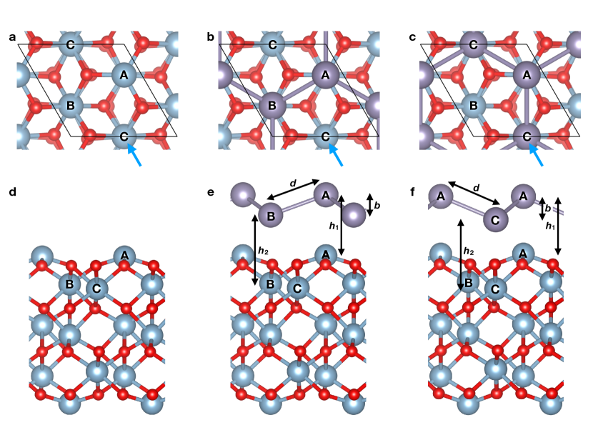
The Al-terminated alumina slab has three exposed aluminum atoms per unit cell, which are labeled A, B, and C in Figure 1(a). Atom A terminates the slab, while atoms B and C are roughly coplanar (0.2 Å vertical separation) and located under a layer of oxygen atoms. We examined a grid of possibly registry alignments for stanene within the alumina unit cell, each of which permits two structures that are obtained by swapping the up-buckled and down-buckled Sn atoms. We relaxed the atomic positions in each of these 18 inequivalent stanene-on-alumina registries. The two most favorable registries, shown in Figures 1(b) and 1(c), place the upper tin atom directly over atom A and the lower tin atom directly over either atom B or C. The structural parameters, binding energies, and DFT-PBE band gaps of the two favorable structures are found in Table 2. The A/C structure is the most energetically favored by a margin of at least 0.24 eV per two-atom stanene unit cell. This structure, which was predicted by similar previous work [28, 29], will be taken as the ground state structure.
III.3 Binding energy and van der Waals functionals
The binding energy equals the total energy of the bound stanene-substrate complex , minus the sum of the energies of the free-standing stanene layer and the bare alumina slab :
| (1) |
To assess the importance of noncovalent interactions in the binding, we calculated both with and without van der Waals dispersion corrections. We checked three van der Waals functionals implemented in Quantum Espresso: the common Grimme DFT-D2 functional [35]; its DFT-D3 revision, which incorporates three-body interactions [37]; and the Becke–Johnson exchange-hole dipole-moment (XDM) model [38, 39]. We found that including a van der Waals functional modifies the interatomic distances listed in Table 2 by less than 0.5%, indicating that the physical structure is determined largely by chemical rather than van der Waals interactions. However, the binding energy, which is 0.50 eV per stanene unit cell without dispersion effects, increase to 0.84–1.23 eV per unit cell depending on the dispersion functional used. The largest binding occurs with the DFT-D2 functional which is known to overbind solids [37], so we expect that the true binding energy lies within the range between the bare and DFT-D2 calculations. A previous study using the optB86b-vdW functional found a binding energy of 1.11 eV per unit cell which is well within this range [28]. This suggests that both noncovalent and covalent interactions are needed to fully describe the absolute magnitude of the binding energy of stanene to alumina.
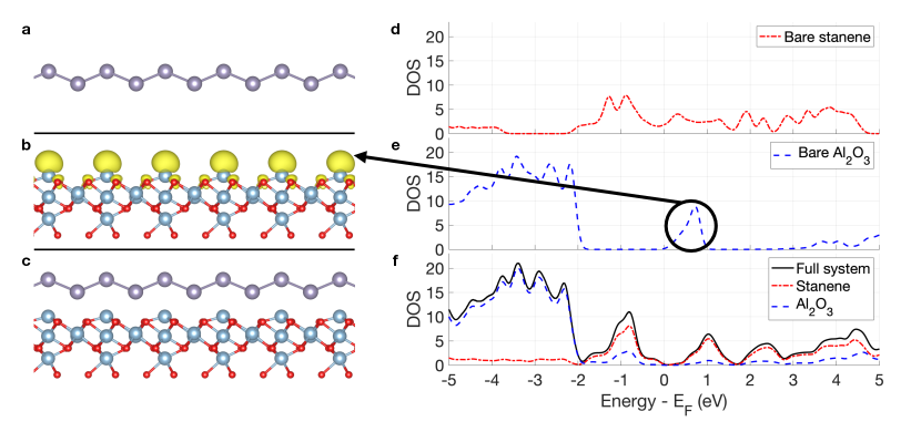
The fact that the chemical binding is quite substantial at 0.50 eV/unit cell requires some explanation: naively, one might expect a wide-gap material such as alumina to be relatively inert. To identify the chemical interaction that drives the binding, we plotted the density of states (DOS) of the free-standing stanene layer, the bare alumina slab, and the stanene-substrate complex (Figures 2(d-f)). The bare alumina slab displays a peak in the DOS just above the Fermi level, which represents a surface state localized to “dangling” orbitals on the top layer of exposed Al atoms (left panel of Figure 2(b)). This state vanishes upon the binding of stanene—as can be seen from Figure 2(f), the states of the full complex near the Fermi level are dominated by Sn orbitals. The unoccupied alumina orbital hybridizes with various Sn orbitals, spreading out in energy over the former alumina gap. In particular, a portion of this orbital forms a new bonding orbital between and 0 eV in Figure 2(f).
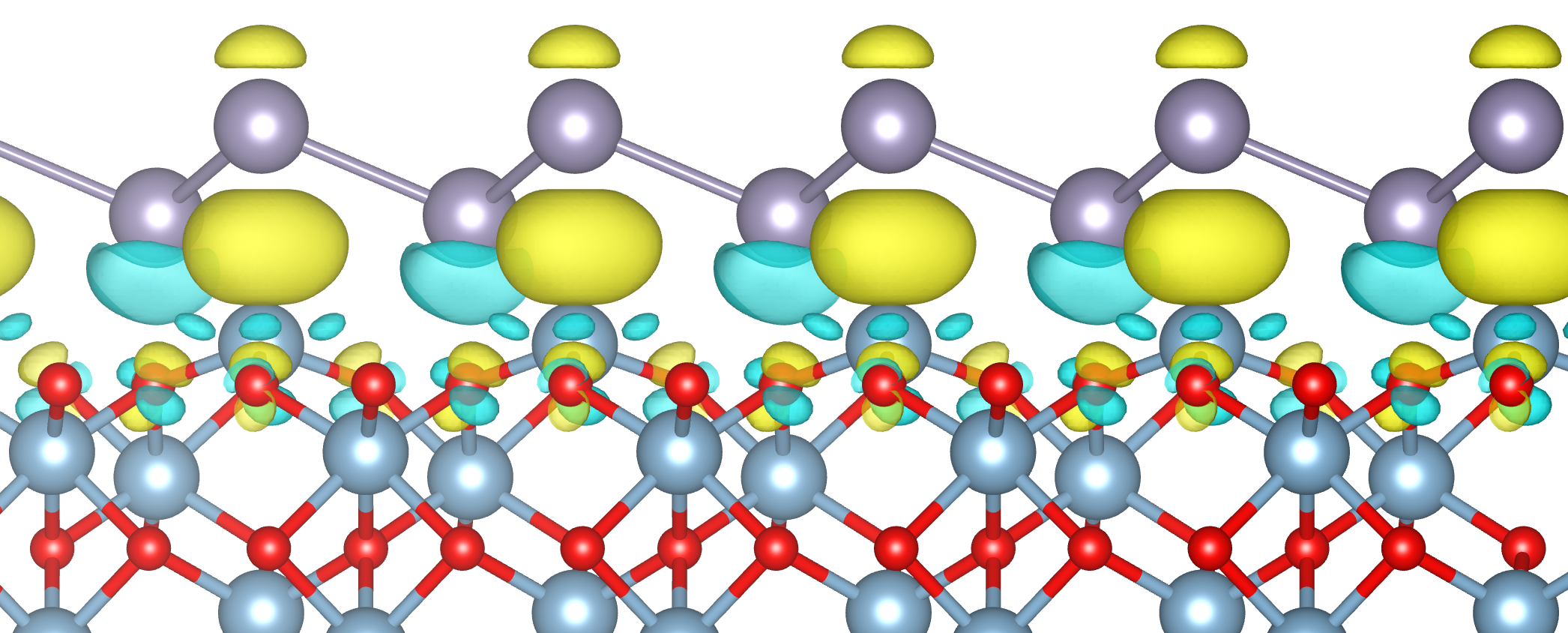
We confirmed that the originally empty “dangling” states of the alumina slab remain localized to the vicinity of the exposed Al atom by examining the redistribution of electron density shown in Figure 3. During binding, electron density redistributes from the cyan regions to the yellow regions, including a large -like region between the surface Al atom and the Sn atom above it. This indicates that the formerly-vacant Al orbital becomes filled as it moves lower in energy and hybridizes with nearby Sn orbitals: a heteropolar covalent bond has formed, explaining the substantial binding energy of 0.50 eV even without van der Waals interactions.
III.4 Commensurate versus incommensurate binding
Since stanene must be placed under 2.4% tensile strain to bind epitaxially to the Al2O3(0001) surface, we checked for the possibility of incommensurate rather than epitaxial binding. In a case of incommensurate binding at the free-standing lattice parameter, the Sn monolayer will be unstrained, but most of the monolayer’s area will not attain its preferred registry with respect to the alumina substrate. Therefore, the competition between epitaxial and incommensurate binding depends on a comparison of the strain energy of the stanene monolayer to the energy penalty for placing the monolayer on a non-optimal registry.
The energy to strain a free-standing stanene monolayer from its equilibrium lattice parameter of to the theoretical Al2O3 lattice parameter of is 25 meV per unit cell. For low strain, an incommensurate overlayer on a substrate can be treated as a long-wavelength superlattice, with each unit cell of the superlattice sampling a different registry. If we label the in-plane position of the lower Sn atom (Sn atoms B or C in Figure 1) by , then the average energy of a single unit cell in such an incommensurate overlayer is approximately
| (2) |
where is the energy of a single commensurate unit cell with a lower Sn atom placed at . We estimate this integral using the registry calculations performed earlier, considering only the grid of structures that are lateral shifts of the optimal A/C structure. The incommensurate energy penalty is 333 meV per unit cell with no van der Waals functional employed, 458 meV per unit cell with the Grimme DFT-D2 functional, and 339 meV per unit cell with the Grimme DFT-D3 functional. In all cases, the incommensurate energy is an order of magnitude greater than the strain energy, so we conclude that the incommensurate structure is irrelevant and that stanene will bind epitaxially on the alumina substrate.
III.5 Dumbbell stanene
We considered the “dumbbell” stanene structure proposed by Tang et al., which contains 10 Sn atoms in a multilayered analogue of a stanene supercell [44]. In an isolated monolayer, out-of-plane hybridization renders dumbbell stanene lower in energy than low-buckled stanene by 0.18 eV per Sn atom [44]. However, we find that dumbbell stanene binds only weakly to Al2O3, collapsing into a disorderly structure that is 0.46 eV per Sn atom higher in energy than the bound low-buckled configuration. This occurs because the highly buckled dumbbell structure prevents a close wetting interaction between Sn atoms and the substrate. Therefore, dumbbell stanene is not a relevant phase when considering epitaxial stanene on alumina.
III.6 Free-standing and bound stanene band structures
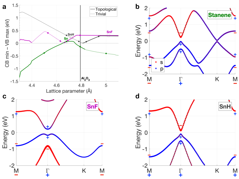
Next, we performed a thorough investigation of the band structures and topological indices of free-standing stanene and its derivatives. Figure 4(a) shows the evolution of the band gaps of free-standing bare stanene, fluorinated stanene, and hydrogenated stanene as a function of lattice parameter, highlighting regimes in which each material is a topological insulator, a topologically nontrivial material with negative gap (defined below), and a topologically trivial metal. For metallic stanene layers, the band structures exhibit a semimetallic negative gap since the conduction band minimum drops below the valence band maximum compared to nearby insulating structures, and for them we compute the topological index that we would obtain if the valence and conduction bands were pulled apart far enough to create a global gap without further modification of the electronic structure. Figures 4(b-d) show the equilibrium band structures of free-standing stanene, fluorinated stanene SnF, and hydrogenated stanene SnH (also called stanane [5]).
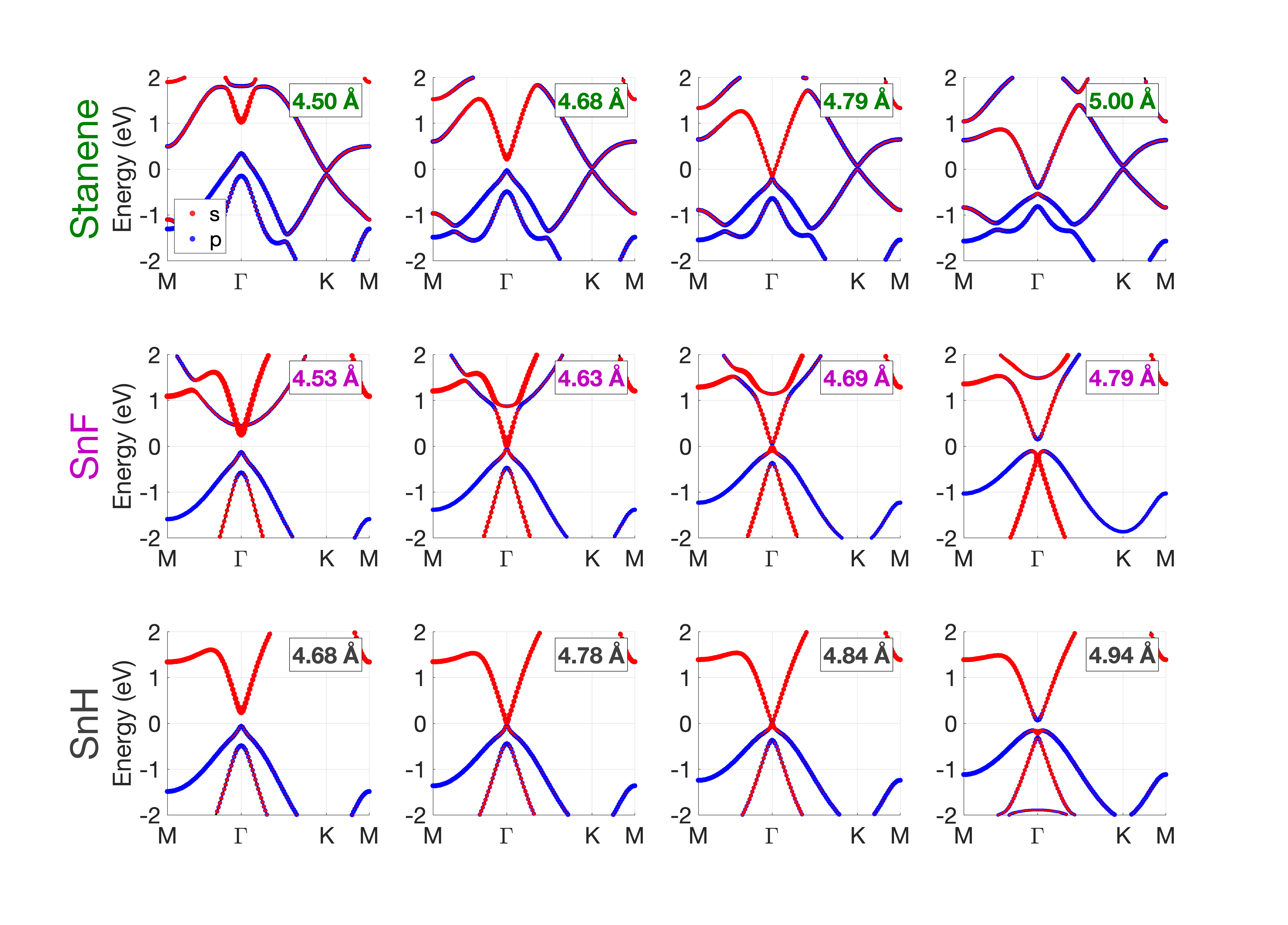
The band structure plots in Figure 5 illustrate how the bands of each material evolve under strain. In the case of bare stanene (top row), the valence band at sits well above the Dirac cone at K when compressive strain is applied (), resulting in a negative-gap semimetal. As the lattice parameter increases (), the gaps at and K line up, forming a globally gapped topological insulator. For small tensile strain (), the gap at is pushed below the Dirac cone at K: this is the regime of strain relevant for stanene on Al2O3, so the substrate is necessary to open the global band gap (we will see that is also sufficient below). Finally, for tensile strain somewhat larger than that applied by Al2O3 (), the gap closes between the negative-parity -type conduction band at and the positive-parity -type valence band (i.e., a band inversion occurs at ). The resulting parity exchange renders free-standing stanene topologically trivial above a lattice parameter of roughly 4.83 Å.
The story is slightly different for SnF and SnH. At their equilibrium lattice parameters, SnF is a topological insulator while SnH is a topologically trivial insulator. However, the two materials are actually quite similar electronically: both materials are trivial insulators under sufficient compressive strain and topological insulators under sufficient tensile strain. The difference between them at equilibrium is simply due to the relative ordering of the lattice parameter of the topological transition and the equilibrium lattice parameter. This can be seen clearly in the middle-row and bottom-row band structures of Figure 5 which depict the topological phase transitions in the two materials. In each case, a negative-parity antibonding band constructed from Sn orbitals moves down through the conduction band, and crosses over to the valence band at , inducing a band inversion and leading to a nontrivial topological index.
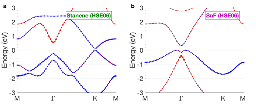
Since each topological phase transition is controlled by a band inversion across the gap at , it is reasonable to ask how robust our results are against a method that accounts better for electron–electron interactions. To check this, we calculated the band structure of relaxed, topologically nontrivial stanene and SnF with VASP [32] using the HSE06 hybrid functional [33, 34], with detailed band structures available in the Appendix (Figure 8). The band gaps in both materials (Figures 4(b,c)) arise from spin–orbit coupling between -states at K and , respectively, so the incorporation of the HSE06 does not change the qualitative shape of the immediately -adjacent bands. The primary qualitative change is that the HSE06 function shifts -states up and -states down at (Table 3). In spite of this change, the proper band inversions are preserved and both materials remain topologically nontrivial under the HSE06 functional.
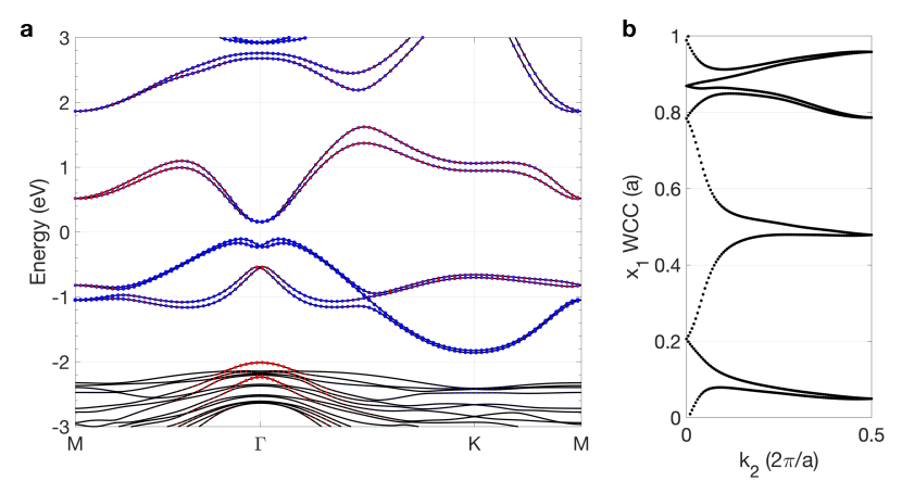
Figure 6(a) shows the the band structure of the full stanene-on-alumina system. It differs from the bare-stanene band structure (Figure 4(b)) in several important ways. First, the presence of the substrate breaks inversion symmetry, which, when combined with the spin-orbit interaction, leads to a Rashba splitting of the conduction bands away from the point. We computed the band structures for stanene on alumina slabs of different thickness and confirmed that the -dependent energy splitting of bands away from the point is due to inversion symmetry breaking (rather than evanescent coupling between the two surfaces of the alumina slab). This data is available in the Appendix.
Finally, the Dirac cone at K has vanished due to the partial saturation of the stanene orbitals by the alumina surface, and the ordering of -type and -type orbitals at has become inverted, yielding a band structure remarkably similar to the free-standing SnF band structure. These features are necessary for the existence of topological behavior in stanene on a substrate [5]. Indeed, we confirmed that stanene on alumina is topologically nontrivial using the Wannier charge center method (Figure 6(b)) [41].
III.7 In situ stanene fluorination
In our final set of calculations, we consider the possibility of in situ functionalization of stanene directly on the Al2O3 surface as a route for future experimental fabrication. As discussed in Section III.F, the Al2O3 substrate and decorating atoms (e.g., F) interact chemically with the Sn hexagonal lattice in analogous ways. Therefore, we expect a fluorinated tin monolayer to take on some structure other than the pristine free-standing SnF sheet on a substrate. However, the pristine structure of isolated SnF should appear if the monolayer is removed from the Al2O3 surface or deposited on a more inert substrate, as it is the ground state of a two-dimensional crystal of stoichiometrically balanced Sn and F. Therefore, a serial process of fluorination followed by exfoliation could, in principle, yield topologically nontrivial SnF via deposition on Al2O3.
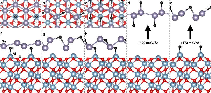
We obtained the ground-state structures for stanene on Al2O3 under fluorine half-functionalization (one F per surface unit cell, Figures 7(a,f)) and full-functionalization (two F per surface unit cell, Figures 7(c,h)). In the fully-functionalized SnF ground state, one F atom sits over the exposed Al atom (site A in the notation of Figure 1), while the other F atom occupies a “bridging” position between the Sn atoms, which remain buckled. The half-fluorinated ground state places the F atom at the exposed Al site, so we infer that this site will be occupied first during fluorination, with the bridging site being filled later. Accommodating the position of the Al-bound F atom requires a registry shift of the stanene sheet (compare Figures 1(c,f)) that, without F present, costs 41 meV/Å2 in energy. The half-fluorinated structure with the F in the bridging position (Figures 7(b,g)) is also an energetic local minimum, but is 0.91 eV per unit cell higher in energy than the Al-bound structure.
Bound, fully fluorinated SnF binds to the alumina surface with a binding energy of 109 meV/Å2, substantially more than the 63 meV/Å2 for bare stanene (see Table 2). For layered bulk materials, both of these binding values lie in the range considered “potentially exfoliable” (Figure 7(d))[45]. One worry we may entertain is that after full-functionalization, the Al-bound F atom could remain in place during exfoliation, yielding a singly-fluorinated Sn sheet (Figure 7(e)). However, from an energetic perspective, this is unlikely: such a structure is 173 meV/Å2 higher in energy than the fully decorated, bound structure, taking it well out of the range of potential exfoliability. Therefore, exfoliation post functionalization with F is expected to produce a fully-fluorinated stanene sheet. Experimental realization of this exfoliation represents an interesting future endeavor.
IV Discussion and outlook
The combination of strong epitaxial binding with band inversion at and -orbital saturation at K indicates that alumina is a promising substrate for the synthesis of bare monolayer stanene. Such a material offers an opportunity for experimental observation of the quantum spin Hall effect [5, 11] as well as a substrate for a variety of technological applications [6, 7, 8, 9, 10]. In addition, the spin separation in the conduction band due to the Rasbha splitting can be harnessed for applications in spintronics and topological superconductivity [46].
Controlled functionalization, e.g., by hydrogen or fluorine, is also an important avenue of stanene research, since functionalization both enhances the band gap and protects against unwanted environmental interactions with Sn orbitals [5]. Generally speaking, two-dimensional materials can be synthesized either by epitaxial deposition or by the exfoliation of multilayered van der Waals materials [1]. The latter method is attractive since it is flexible and modular, but is impractical for materials like bare stanene whose 3D bulk phase (-tin) is not intrinsically layered. As we showed in Section III.G, introducing fluorine to a bound stanene monolayer is expected to form a functonalized tin sheet that may be exfoliable for use in heterostructure and device applications.
In summary, we have shown that monolayer stanene binds strongly and epitaxially to the Al2O3(0001) surface, with a buckled structure and a sizable global band gap. We have examined the chemical character of the binding and verified the topologically nontrivial nature of stanene on alumina. With its wide surface band gap and relative inertness, alumina is a promising substrate for future experimental fabrication and characterization.
Acknowledgements.
This work was supported by Function Accelerated nanoMaterial Engineering (FAME), AFOSR, No. FA9550-15-1-0472. It also used the Extreme Science and Engineering Discovery Environment (XSEDE), which is supported by National Science Foundation grant number ACI-1548562, via computer time on the Comet supercomputer as enabled by XSEDE allocation MCA08X007. S.E. also acknowledges support from the NSF Graduate Research Fellowship, No. DGE1752134. Atomic structural images were produced with the VESTA package [47].*
Appendix A Additional calculations
Figure 8 shows the band structures of bare and fluorinated stanene computed using the HSE06 hybrid functional. Bands are labeled by their (red) and (blue) character to demonstrate that the band ordering that ensures the topological character of each material is preserved, even when better accounting for nonlocal electron-electron interactions.
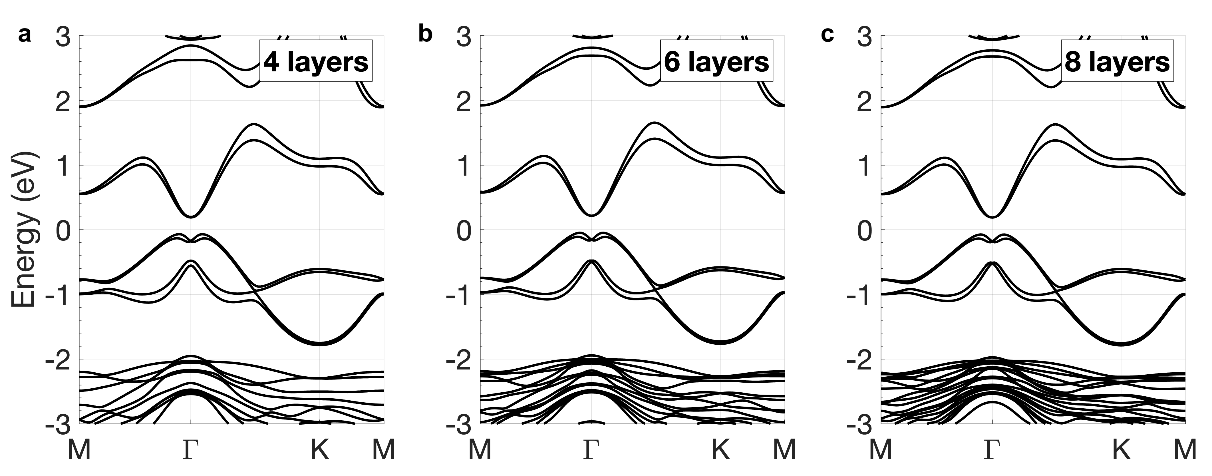
Figure 9 compares the band structures of stanene on 4-, 6-, and 8-layer alumina slabs. Below around eV, an increasing density of bulk bands can be seen, but the near- states, localized to the tin overlayer, are unaffacted by the thickness of the substrate.
| Stanene | PBE | HSE06 | SnF | PBE | HSE06 |
|---|---|---|---|---|---|
| Valence – splitting @ | Valence – splitting @ | ||||
| Valence – difference @ | Valence – difference @ | ||||
| Direct band gap @ K |
References
- Molle et al. [2017] A. Molle, J. Goldberger, M. Houssa, Y. Xu, S.-C. Zhang, and D. Akinwande, Buckled two-dimensional Xene sheets, Nature Materials 16, 163 (2017).
- Lyu et al. [2019] J. Lyu, S. Zhang, C. Zhang, and P. Wang, Stanene: A Promising Material for New Electronic and Spintronic Applications, Annalen der Physik 531, 1900017 (2019).
- Sahoo and Wei [2019] S. K. Sahoo and K. Wei, A Perspective on Recent Advances in 2D Stanene Nanosheets, Advanced Materials Interfaces 6, 1900752 (2019).
- Ma et al. [2012] Y. Ma, Y. Dai, M. Guo, C. Niu, and B. Huang, Intriguing Behavior of Halogenated Two-Dimensional Tin, The Journal of Physical Chemistry C 116, 12977 (2012).
- Xu et al. [2013] Y. Xu, B. Yan, H.-J. Zhang, J. Wang, G. Xu, P. Tang, W. Duan, and S.-C. Zhang, Large-Gap Quantum Spin Hall Insulators in Tin Films, Physical Review Letters 111, 136804 (2013).
- Zheng et al. [2018] J. Zheng, F. Chi, and Y. Guo, Spin-current diodes based on germanene and stanene subjected to local exchange fields, Applied Physics Letters 113, 112404 (2018).
- Marin et al. [2018] E. G. Marin, D. Marian, G. Iannaccone, and G. Fiori, Tunnel-Field-Effect Spin Filter from Two-Dimensional Antiferromagnetic Stanene, Physical Review Applied 10, 044063 (2018).
- Vandenberghe and Fischetti [2017] W. G. Vandenberghe and M. V. Fischetti, Imperfect two-dimensional topological insulator field-effect transistors, Nature Communications 8, 14184 (2017).
- Abbasi [2019a] A. Abbasi, Modulation of the electronic properties of pristine and AlP-codoped stanene monolayers by the adsorption of CHO and CH molecules: a DFT study, Materials Research Express 6, 076410 (2019a).
- Abbasi [2019b] A. Abbasi, Theoretical Investigation of The interaction Between Noble Metals (Ag, Au, Pd, Pt) and Stanene Nanosheets: A DFT Study, Journal of Inorganic and Organometallic Polymers and Materials 29, 1895 (2019b).
- Zhang et al. [2017] H. Zhang, Z. Wang, and X. Xu, Room temperature quantum spin Hall insulator: Functionalized stanene on layered PbI substrate, Applied Physics Letters 111, 072105 (2017).
- Wu et al. [2014] S.-C. Wu, G. Shan, and B. Yan, Prediction of Near-Room-Temperature Quantum Anomalous Hall Effect on Honeycomb Materials, Physical Review Letters 113, 256401 (2014).
- Matusalem et al. [2016] F. Matusalem, F. Bechstedt, M. Marques, and L. K. Teles, Quantum spin Hall phase in stanene-derived overlayers on passivated SiC substrates, Physical Review B 94, 241403(R) (2016).
- Li [2019] P. Li, Stanene on a SiC(0001) surface: a candidate for realizing quantum anomalous Hall effect, Physical Chemistry Chemical Physics 21, 11150 (2019).
- Xu et al. [2015] Y. Xu, P. Tang, and S.-C. Zhang, Large-gap quantum spin Hall states in decorated stanene grown on a substrate, Physical Review B 92, 081112(R) (2015).
- Yuhara et al. [2018] J. Yuhara, Y. Fujii, K. Nishino, N. Isobe, M. Nakatake, L. Xian, A. Rubio, and G. Le Lay, Large area planar stanene epitaxially grown on Ag(111), 2D Materials 5, 025002 (2018).
- Ogikubo et al. [2020] T. Ogikubo, H. Shimazu, Y. Fujii, K. Ito, A. Ohta, M. Araidai, M. Kurosawa, G. Le Lay, and J. Yuhara, Continuous Growth of Germanene and Stanene Lateral Heterostructures, Advanced Materials Interfaces 7, 1902132 (2020).
- Liu et al. [2019] Y. Liu, N. Gao, J. Zhuang, C. Liu, J. Wang, W. Hao, S. X. Dou, J. Zhao, and Y. Du, Realization of Strained Stanene by Interface Engineering, The Journal of Physical Chemistry Letters 10, 1558 (2019).
- Pang et al. [2020] W. Pang, K. Nishino, T. Ogikubo, M. Araidai, M. Nakatake, G. Le Lay, and J. Yuhara, Epitaxial growth of honeycomb-like stanene on Au(111), Applied Surface Science 517, 146224 (2020).
- Gou et al. [2017] J. Gou, L. Kong, H. Li, Q. Zhong, W. Li, P. Cheng, L. Chen, and K. Wu, Strain-induced band engineering in monolayer stanene on Sb(111), Physical Review Materials 1, 054004 (2017).
- Zhu et al. [2015] F.-f. Zhu, W.-j. Chen, Y. Xu, C.-l. Gao, D.-d. Guan, C.-h. Liu, D. Qian, S.-C. Zhang, and J.-f. Jia, Epitaxial growth of two-dimensional stanene, Nature Materials 14, 1020 (2015).
- Li et al. [2020a] J. Li, T. Lei, J. Wang, R. Wu, J. Zhao, L. Zhao, Y. Guo, H. Qian, and K. Ibrahim, Anisotropic Electronic Structure and Interfacial Chemical Reaction of Stanene/BiTe, The Journal of Physical Chemistry C 124, 4917 (2020a).
- Li et al. [2020b] J. Li, T. Lei, J. Wang, R. Wu, H. Qian, and K. Ibrahim, In-plane crystal field constrained electronic structure of stanene, Applied Physics Letters 116, 101601 (2020b).
- Deng et al. [2018] J. Deng, B. Xia, X. Ma, H. Chen, H. Shan, X. Zhai, B. Li, A. Zhao, Y. Xu, W. Duan, S.-C. Zhang, B. Wang, and J. G. Hou, Epitaxial growth of ultraflat stanene with topological band inversion, Nature Materials 17, 1081 (2018).
- Zang et al. [2018] Y. Zang, T. Jiang, Y. Gong, Z. Guan, C. Liu, M. Liao, K. Zhu, Z. Li, L. Wang, W. Li, C. Song, D. Zhang, Y. Xu, K. He, X. Ma, S.-C. Zhang, and Q.-K. Xue, Realizing an Epitaxial Decorated Stanene with an Insulating Bandgap, Advanced Functional Materials 28, 1802723 (2018).
- Xu et al. [2018] C.-Z. Xu, Y.-H. Chan, P. Chen, X. Wang, D. Flototto, J. A. Hlevyack, G. Bian, S.-K. Mo, M.-Y. Chou, and T.-C. Chiang, Gapped electronic structure of epitaxial stanene on InSb(111), Physical Review B 97, 035122 (2018).
- Zheng et al. [2019] X. Zheng, J.-F. Zhang, B. Tong, and R.-R. Du, Epitaxial growth and electronic properties of few-layer stanene on InSb(111), 2D Materials 7, 011001 (2019).
- Wang et al. [2016] H. Wang, S. T. Pi, J. Kim, Z. Wang, H. H. Fu, and R. Q. Wu, Possibility of realizing quantum spin Hall effect at room temperature in stanene/AlO(0001), Physical Review B 94, 035112 (2016).
- Araidai et al. [2017] M. Araidai, M. Kurosawa, A. Ohta, and K. Shiraishi, First-principles study on adsorption structure and electronic state of stanene on -alumina surface, Japanese Journal of Applied Physics 56, 095701 (2017).
- Giannozzi et al. [2009] P. Giannozzi, S. Baroni, N. Bonini, M. Calandra, R. Car, C. Cavazzoni, D. Ceresoli, G. L. Chiarotti, M. Cococcioni, I. Dabo, A. Dal Corso, S. de Gironcoli, S. Fabris, G. Fratesi, R. Gebauer, U. Gerstmann, C. Gougoussis, A. Kokalj, M. Lazzeri, L. Martin-Samos, N. Marzari, F. Mauri, R. Mazzarello, S. Paolini, A. Pasquarello, L. Paulatto, C. Sbraccia, S. Scandolo, G. Sclauzero, A. P. Seitsonen, A. Smogunov, P. Umari, and R. M. Wentzcovitch, QUANTUM ESPRESSO: a modular and open-source software project for quantum simulations of materials, Journal of Physics: Condensed Matter 21, 395502 (2009).
- Perdew et al. [1996] J. P. Perdew, K. Burke, and M. Ernzerhof, Generalized gradient approximation made simple, Physical Review Letters 77, 3865 (1996).
- Kresse and Furthmüller [1996] G. Kresse and J. Furthmüller, Efficiency of ab-initio total energy calculations for metals and semiconductors using a plane-wave basis set, Computational Materials Science 6, 15 (1996).
- Heyd et al. [2003] J. Heyd, G. E. Scuseria, and M. Ernzerhof, Hybrid functionals based on a screened Coulomb potential, The Journal of Chemical Physics 118, 8207 (2003).
- Krukau et al. [2006] A. V. Krukau, O. A. Vydrov, A. F. Izmaylov, and G. E. Scuseria, Influence of the exchange screening parameter on the performance of screened hybrid functionals, The Journal of Chemical Physics 125, 224106 (2006).
- Grimme [2006] S. Grimme, Semiempirical GGA-type density functional constructed with a long-range dispersion correction, Journal of Computational Chemistry 27, 1787 (2006).
- Barone et al. [2009] V. Barone, M. Casarin, D. Forrer, M. Pavone, M. Sambi, and A. Vittadini, Role and effective treatment of dispersive forces in materials: Polyethylene and graphite crystals as test cases, Journal of Computational Chemistry 30, 934 (2009).
- Grimme et al. [2010] S. Grimme, J. Antony, S. Ehrlich, and H. Krieg, A consistent and accurate ab initio parametrization of density functional dispersion correction (DFT-D) for the 94 elements H–Pu, The Journal of Chemical Physics 132, 154104 (2010).
- Becke and Johnson [2007] A. D. Becke and E. R. Johnson, Exchange-hole dipole moment and the dispersion interaction revisited, The Journal of Chemical Physics 127, 154108 (2007).
- Otero-de-la Roza and Johnson [2012] A. Otero-de-la Roza and E. R. Johnson, Van der Waals interactions in solids using the exchange-hole dipole moment model, The Journal of Chemical Physics 136, 174109 (2012).
- Fu and Kane [2007] L. Fu and C. L. Kane, Topological insulators with inversion symmetry, Physical Review B 76, 045302 (2007).
- Soluyanov and Vanderbilt [2011] A. A. Soluyanov and D. Vanderbilt, Computing topological invariants without inversion symmetry, Physical Review B 83, 235401 (2011).
- Wu et al. [2018] Q. Wu, S. Zhang, H.-F. Song, M. Troyer, and A. A. Soluyanov, WannierTools: An open-source software package for novel topological materials, Computer Physics Communications 224, 405 (2018).
- Pizzi et al. [2020] G. Pizzi, V. Vitale, R. Arita, S. Blügel, F. Freimuth, G. Géranton, M. Gibertini, D. Gresch, C. Johnson, T. Koretsune, J. Ibañez-Azpiroz, H. Lee, J.-M. Lihm, D. Marchand, A. Marrazzo, Y. Mokrousov, J. I. Mustafa, Y. Nohara, Y. Nomura, L. Paulatto, S. Poncé, T. Ponweiser, J. Qiao, F. Thöle, S. S. Tsirkin, M. Wierzbowska, N. Marzari, D. Vanderbilt, I. Souza, A. A. Mostofi, and J. R. Yates, Wannier90 as a community code: new features and applications, Journal of Physics: Condensed Matter 32, 165902 (2020).
- Tang et al. [2014] P. Tang, P. Chen, W. Cao, H. Huang, S. Cahangirov, L. Xian, Y. Xu, S.-C. Zhang, W. Duan, and A. Rubio, Stable two-dimensional dumbbell stanene: A quantum spin Hall insulator, Physical Review B 90, 121408(R) (2014).
- Mounet et al. [2018] N. Mounet, M. Gibertini, P. Schwaller, D. Campi, A. Merkys, A. Marrazzo, T. Sohier, I. E. Castelli, A. Cepellotti, G. Pizzi, and N. Marzari, Two-dimensional materials from high-throughput computational exfoliation of experimentally known compounds, Nature Nanotechnology 13, 246 (2018).
- Wang et al. [2014] J. Wang, Y. Xu, and S.-C. Zhang, Two-dimensional time-reversal-invariant topological superconductivity in a doped quantum spin-Hall insulator, Physical Review B 90, 054503 (2014).
- Momma and Izumi [2011] K. Momma and F. Izumi, VESTA 3 for three-dimensional visualization of crystal, volumetric and morphology data, Journal of Applied Crystallography 44, 1272 (2011).