canfield@ameslab.gov]
Evidence for large Rashba splitting in PtPb4 from Angle-Resolved Photoemission Spectroscopy
Abstract
We studied the electronic structure of PtPb4 using laser angle-resolved photoemission spectroscopy(ARPES) and density functional theory(DFT) calculations. This material is closely related to PtSn4, which exhibits exotic topological properties such as Dirac node arcs. Fermi surface(FS) of PtPb4 consists of two electron pockets at the center of the Brillouin zone(BZ) and several hole pockets around the zone boundaries. Our ARPES data reveals significant Rashba splitting at the point in agreement with DFT calculations. The presence of Rashba splitting may render this material of potential interest for spintronic applications.
I INTRODUCTION
Recently, the search for new topological materials has resulted in a number of discoveries of very interesting materials, and has become a popular trend in condensed matter physics. Unique topological states such as spin-momentum locking[1], conductive surface state[2], back scattering suppression[3], Fermi arc[4] and surface states protected by time-reversal symmetry[2, 5] offer promise of a wide range of applications and significant advancement of computing technologies [6, 7, 8, 9, 10, 11]. The ability to generate spin currents in topological materials is very important for spintronic applications[11]. The search for novel topological materials often starts with theoretical investigations such as DFT calculations later confirmed by experimental studies[12, 4, 13, 14, 15].
Recent measurements of the band structure in PtSn4 revealed Dirac node arcs which are with Dirac-like dispersions extending along one dimensional line instead of having cylindrical symmetry[16]. PtSn4 is composed of Sn-Pt-Sn layers along the axis with orthorhombic structure[17]. This is a rare example of the discovery of a topological material done by experiment rather than theory.
Building on our success with PtSn4, we undertook an investigation of related materials to understand the origin of the Dirac node arc. We examined transport properties and band structures of PdSn4, which belongs to the same structural family as PtSn4[18]. In the case of PdSn4, the Dirac node arc disappears but the single Dirac cone still persists upon replacing Pt with Pd. This might indicate that the Dirac node arc could be sensitive to spin-orbit coupling(SOC).
To better understand the properties of PtSn4 and structurally related ultra-heavy compounds with large SOC, we studied the electronic structure of PtPb4. Interestingly, this material is a superconductor with of 2.4 K [19]. In addition, it is an efficient electrocatalyst used in hydrogen fuel cells, which are important for renewable energy[20, 6]. PtPb4 crystallizes in a tetragonal structure that is qualitatively very similar to the structure of PtSn4. PtPb4 is composed of Pb-Pt-Pb slabs that are simliar to the Sn-Pt-Sn slabs in PtSn4. PtPb4 has lattice constants 6.667 Å and 5.978 Å [21] and is predicted to be a strong topological insulator. Although PtSn4 and structurally related systems have been studied intensively, PtPb4 has eluded experimental studies of its electronic properties. Here, we report the electronic structure of PtPb4 by using ultrahigh-resolution ARPES and DFT calculations. We found more than two electron pockets at the center of the BZ and several hole pockets around zone boundaries of each direction. Intriguingly, our ARPES data shows 2-fold symmetry even though the crystal structure is tetragonal. X-ray data and DFT calculations show that this is due to a modified stacking of the Pb-Pt-Pb layers of the material.
.
Our measurements reveal large Rashba splitting (RS) at a binding energy of 1.3 eV. RS is a breaking of spin degeneracy as a result of SOC and inversion symmetry breaking. Although SOC appears various systems, it is stronger in materials including high-Z elements due to relatively larger spin-orbit parameter. Since RS is a spin-polarized surface state, it is expected to be useful in a generation of spin currents and manipulation of spin polarization by electric field for spintronic devices[22]. Despite decades of research, the operation of spintronic devices is very limited to low temperatures. Previous research demonstrates that spin-injected field effect transistor (spin FET) controlled by gate voltage operates at 1.8 K[23] and the spin Hall effect transistor works at 4 K [24]. One of the major turning points in spintronic devices is using spin-polarized state of large RS. It was initially discussed in a wurtzite structure[25] and intensively studied in various metals[26, 27, 28], some alloys[29, 30], thin films[31, 32, 33], and semiconductors[34, 35, 36] which show giant Rashba splitting. Semiconductors typically show small RS, which is not suitable for room temperature spintronic devices. On the other hand, metals show relatively large RS but the spin polarization cannot be controlled by an external electric field. Our ARPES data and DFT calculations show that the RS in PtPb4 is comparable to those of metal surface states. New generation spintronics devices working at room temperature need large splitting between spin polarized bands and demand tunability of chemical potential. Consequently, the spin polarized surface state in PtPb4 gives us a chance to control the spin without applying magnetic fields at room temperature, paving a way for developing more efficient spintronics devices.
II METHODS
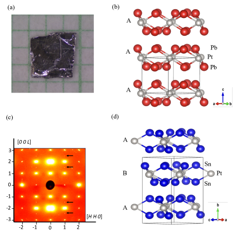
Single crystals of PtPb4 were grown out of Pb-rich binary melts. [37] We put three different initial stoichiometries of Pt13Pb87, Pt11Pb89, and Pt9Pb91 into fritted alumina crucibles [CCS], [38] and then sealed it into amorphous silica tubes under partial Ar atmosphere. The ampoules were heated up to 600 ∘C, held there for 5 hours, rapidly cooled to 375 ∘C and then slowly cooled down to 310 ∘C over more than 100 hours, and then finally decanted using a centrifuge. The single crystalline samples have a clear plate like shape with a mirrored surface. Fig.1a shows a photograph of a single crystal of PtPb4 on a millimeter scale. typical crystals have dimensions of 3 mm 3 mm 0.5 mm. The crystallographic axis is perpendicular to the platelike plane.
High-energy X-ray diffraction measurements were performed at station 6-ID-D at the Advanced Photon Source, Argonne National Laboratory. Measurements were made using 100 keV X-rays, with the incident beam direction normal to the reciprocal-lattice planes. Diffraction patterns were recorded using a MAR345 area detector. Unlike laboratory sources, high-energy X-rays ensure that the bulk of the sample is probed. By rocking the sample through small angular ranges about the axes perpendicular to the incident beam, we obtain an image of the reciprocal-lattice planes normal to the incident beam direction [39].
The density functional theory (DFT) [40] calculations are performed using the Vienna Ab-initio Simulation Package (VASP) [41] with projector-augmented wave (PAW) pseudo-potential method [42][43] within generalized-gradient approximation (GGA) [44]. The energy cutoff is 300 eV and the Monkhost-Pack scheme [45] is used for Brillouin zone sampling with a high quality k-point mesh of 8 8 8 for tetragonal PtPb4 and 8 4 8 for orthorhombic PtPb4 structures, respectively. All structures are fully relaxed until the forces acting on each atom are smaller than 0.01 eV/Å and all stress tensor elements are smaller than 1 kbar (0.1 GPa). Since both Pt and Pb are heavy elements, the relativistic effect is not negligible and is taken into account via spin-orbit coupling (SOC) calculations. The van der Waals (vdW) interaction is also taken into account by the DFT-D3 method [46],[47]. The surface formation energy is calculated by a slab model. The slab model consists 6 PtPb4 layers with two identical surfaces [(001) for the tetragonal and (010) for the orthorhombic structures] and a vacuum region of more than 20 Å in the direction perpendicular to the surfaces to avoid interaction between the slab and its images due to periodic boundary conditions. A supercell of 2 2 in the lateral directions is used containing 60 atoms. The 2 center layers are kept fixed at bulk atomic positions while atomic positions of the 2 outer most layers for each surface are relaxed. SOC and vdW interactions are included in the surface formation energy calculation.
ARPES measurements were carried out using a laboratory based tunable VUV laser. The ARPES system consists of a Scienta R8000 electron analyzer, picosecond Ti:Sapphire oscillator and fourth-harmonic generator [48]. All data were collected with 6.7 eV photon energy. Angular resolution was set at ∼0.1∘ and 1∘, respectively, and the energy resolution was set at 2 meV. The size of the photon beam on the sample was m. Samples were cleaved in-situ at a base pressure lower than 1 10-10 Torr, 40 K and kept at the cleaving temperature throughout the measurement.
III RESULTS AND DISCUSSION
The previously reported crystal structure of PtPb4 consists of stacked Pb-Pt-Pb layers along the axis as shown in Fig.1(b). The grey spheres represent Pt atoms, and red spheres are Pb atoms. High-energy X-ray diffraction data were taken on a single crystal sample of PtPb4 as seen in Fig.1.(c) to search for any structural anomalies such as orthohombicity. No peak broadening or splitting was observed, but additional peaks are clearly observed at half positions of in Fig.1.(c), which are marked by black arrows. These peaks are forbidden for the reported space group of PtPb4 and the resulting reflection conditions are not consistent with any tetragonal space group. However, several orthorhombic crystal structures like e.g. PtSn4, would be consistent with the observed doubling of the unit cell in direction indicated by the additional half-integer Bragg peaks and the observed reflection conditions. Fig.1 (d) shows the most closely related oS20 of PtSn4 type structure by simply changing the stacking order. Grey balls represent Pt atoms and blue ones are Sn atoms.
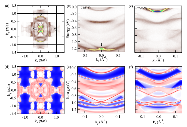
Our key experimental results are presented in Figs.2 and 3. We see a clear RS and find a surprising symmetry rather than symmetry in the plane. Given the fact that we observe additional peaks at half positions of in the X-ray data, we performed the ARPES measurement to understand the origin of these additional peaks. The FS and band dispersion along key directions in the BZ for PtPb4 are shown in Figs.2(a)-(c). Fig.2(a) shows the ARPES intensity integrated within 10 meV about the chemical potential, which roughly visualizes the FS. The FS consists of at least one electron pocket at the center of the BZ and is surrounded by several other electron pockets. Previous results[49] show that the crystal structure of PtPb4 has AA stacking of PtPb4 slabs along the tetragonal c-axis with the space group . However, our X-ray and ARPES data point to the possibility of slight distortion of the crystal structure due to observed symmetry of the Fermi surface. Figs.2.(d)-(f) show the calculated FS and band dispersion based on oS20 structure with AB stacking of PtPb4 slabs (with A and B being shifted in the basal plane with respect to each other) with the lattice constant doubled in direction. In the calculation, we used the PtSn4 structure wtih 2 fold symmetry because it is shown to be energetically close to the PtPb4 structure. Results seem to be in a good agreement with the ARPES data. The measured FS shows significant differences between the x and y directions and pockets around the X and Y points clearly have different shapes. Despite the tetragonal crystal structure of PtPb4, the ARPES and X-ray scattering data indicate that the band structure at the surface may have different electronic properties than in the bulk. In order to understand this discrepancy between expectations based on the bulk crystal structure and ARPES measurements, we performed extensive band structure calculations.
| GGA-PBE | GGA-PBEsol | |
|---|---|---|
| w-SOC | 2.2 | 1.3 |
| w-SOC-vdW | -1.3 | -4.3 |
Given that we see some evidence for 2-fold symmetry in our ARPES data, we used DFT calculations to determine how energetically removed the possibility of tetragonal structure in PtPb4. To be more specific, Table 1 shows the energy difference of - between tetragonal and orthorhombic PtPb4 phases without the inclusion of the vdW interactions. It shows that the orthorhombic phase is more stable by -2.2 meV/atom. We also perform a calculation using revised-GGA (PBEsol) [50] to verify the calculated relative stability and find that the orthorhombic phase is also more stable within this approximation. We note that both tetragonal and orthorhombic phases are layered structures with a gap of 3.1 Å between Pb-terminated layers. Therefore, the vdW interactions would play an important role in determining the stability of different phases in this material. With the vdW interactions taken into account, it turns out that the tetragonal phase becomes more stable than the orthorhombic phase by -1.3 and -4.3 meV/atom for PBE and PBEsol GGA calculations. However, the energy differences, with and without vdW interaction correction, are very small within the order of a few K in term of thermal energy. In addition, the surface formation energies of these two phases are also very similar, which are 27.23 and 27.95 meV/ for orthorhombic and tetragonal phases, respectively. The orthorhombic phase has a slightly lower surface formation energy. Therefore, it is very likely that PtPb4 is polymorphic and orthorhombic PtPb4 can be stabilized close to the surface. Based on the X-ray data, DFT calculations and the ARPES measurement, the actual surface may contain a mixture of domains with different terminations.
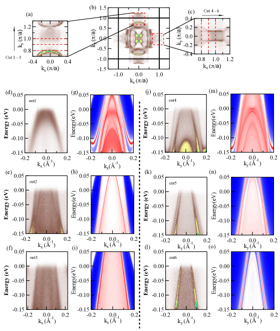
In Fig.3, we focus on the FS and band dispersion in the proximity of the X and Y points. An enlarged image from the red boxes in Fig.3(b) is shown in Fig.3(a) and Fig.3(c). Close to the X point, the FS has two parallel sections that consist of two merged hole-like bands as shown in Figs.3(c) and (j-l). Both bands are quite sharp and intense, which is consistent with a surface origin. The measured band dispersion in this part of the zone agrees quite well with the DFT calculations shown in Figs.3(m)-(o). The parallel FS due to surface bands bare some resemblance to PtSn4 and PdSn4[16, 18], although no topological features below are observed here; PtSn4 has Dirac node arcs surface states but PtPb4 shows a linear-like dispersion close to the X point.
The band structure near the Y point is shown in Figs.3 (b) and (d-f), while Figs.3 (g)-(i) show DFT calculations in the same part of the BZ. The ARPES intensity in this part of the BZ is weaker and bands are much broader, pointing to mostly a bulk origin that causes broadening due to the projection along . The bands with strong surface components predicted by calculations Figs.3(h, i) are not well seen, which may indicate that matrix elements likely play a role in suppressing the signal.
We found a clear RS of the valence band. It depicts spin degeneracy lifting at surfaces or interfaces, where inversion symmetry is broken with spin-orbit interaction, which may lead to an asymmetric charge distribution. Relation between the breaking of spin degeneracy and the inversion symmetry can be described by the relativistic effect of moving electrons in a two-dimensional momentum space. The interaction between electron spin and effective magnetic field, originating from a surface electrostatic field, leads to a Zeeman splitting. As a consequence, the degeneracy is lifted and chiral spin texture in band dispersion and maxima of the valence band or minima of conduction band are shifted from the symmetry point. Despite the reasonable success of initially proposed effective model[25, 51], this model shows several limitations as well. The most important issue is the magnitude of the splitting. A result based on the effective model shows that the magnitude of splitting is, at least, several orders of magnitude smaller than that of previously observed data. On top of that, the effective model cannot explain the fact that SOC is stronger in high-Z elements because the strength of electric fields from the surfaces is roughly in the same order of magnitude. Recently, there are several attempts to explain this phenomenon by using numerical and analytic methods[52, 53]. Those results point out that RS may be related to the combination of an orbital angular momentum state and electron momentum that introduces asymmetric charge distribution. Although spin-orbit interaction occurs very often in various materials either in bulk or surface states, it is more pronounced in systems including high-Z elements due to relatively large spin-orbit parameter.
In spite of the breaking of symmetry, which may cause anisotropic spin-orbit coupling, we observed the RS in the -Y direction. In some materials, it is not easy to distinguish a Rashba and Dresselhaus splitting experimentally. In order to understand the origin of the band splitting, we performed DFT calculations. Based on the calculation results, we verify that the band splitting occurs at the surface state. The black arrow in Fig.2 (b) shows the position of the RS in the ARPES data. It clearly shows the RS with a valence band minimum (VBM) of = 1.3 eV at the momentum offsets of with = 0.04 around the . This result shows that the RS in this material is several times bigger than that of Au(111)[54], which is the initially reported ARPES measurement of a RS. In our ARPES data, the VBM is slightly lower than predicted by calculation. Fig.2 (c) shows the band dispersion along the -X direction. We find at least one electron pocket in this direction. Figs.2 (e) and (f) show DFT calculations of -Y and -X cuts and bare resemblance to the ARPES data modulo a small shift in the energy, which is quite typical.
The outstanding issue is the difference between the observed two-fold symmetry of the band structure and the four fold symmetry of the crystal structure of PtPb4. Our DFT calculations and X-ray data led us to conclude that the symmetry breaking may be caused by an ABAB stacking sequence; the orthorhombic structure is more favorable. Lastly, we observed a RS, at the center of the BZ, which typically appears at the surface or interface of materials. Even though this effect occurs below , it may be possible by either chemical substitution or gating to move the chemical potential down to utilize this effect in a generation of spin currents at room temperature. This may have interesting consequences not only due to its fundamental importance but also its possibility of application for spintronic devices.
IV ACKNOWLEDGMENTS
This work was supported by the U.S. Department of Energy, Office of Science, Basic Energy Sciences, Materials Science and Engineering Division. Ames Laboratory is operated for the U.S. Department of Energy by Iowa State University under contract No. DE-AC02-07CH11358. K. L. was supported by CEM, an NSF MRSEC, under grant DMR-1420451. This research used resources of the Advanced Photon Source, a U.S. Department of Energy (DOE) Office of Science User Facility operated for the DOE Office of Science by Argonne National Laboratory under Contract No. DE-AC02-06CH11357.
References
- Kane and Moore [2011] C. Kane and J. Moore, Topological insulators, Physics World 24, 32 (2011).
- Hasan and Kane [2010] M. Z. Hasan and C. L. Kane, Colloquium: topological insulators, Reviews of modern physics 82, 3045 (2010).
- Qi and Zhang [2010] X.-L. Qi and S.-C. Zhang, The quantum spin Hall effect and topological insulators, arXiv preprint arXiv:1001.1602 (2010).
- Xu et al. [2015a] S.-Y. Xu, I. Belopolski, N. Alidoust, M. Neupane, G. Bian, C. Zhang, R. Sankar, G. Chang, Z. Yuan, C.-C. Lee, et al., Discovery of a Weyl fermion semimetal and topological Fermi arcs, Science 349, 613 (2015a).
- Moore [2010] J. E. Moore, The birth of topological insulators, Nature 464, 194 (2010).
- Li et al. [2019] G. Li, C. Fu, W. Shi, L. Jiao, J. Wu, Q. Yang, R. Saha, M. E. Kamminga, A. K. Srivastava, E. Liu, et al., Dirac nodal arc semimetal PtSn4: An ideal platform for understanding surface properties and catalysis, Angewandte Chemie (2019).
- Belyakov and Gourlay [2014] S. Belyakov and C. Gourlay, Heterogeneous nucleation of -Sn on NiSn4, PdSn4 and PtSn4, Acta Materialia 71, 56 (2014).
- Kuhmann et al. [1998] J. F. Kuhmann, C.-H. Chiang, P. Harde, F. Reier, W. Ö österle, I. Urban, and A. Klein, Pt thin-film metallization for FC-bonding using SnPb60/40 solder bump metallurgy, Materials Science and Engineering: A 242, 22 (1998).
- Kempf and Schmauder [1998] B. Kempf and S. Schmauder, Thermodynamic modelling of precious metals alloys, Gold Bulletin 31, 51 (1998).
- Biggs et al. [2005] B. T. Biggs, S. Taylor, and E. Van der Lingen, The hardening of platinum alloys for potential jewellery application, Platinum Metals Review 49, 2 (2005).
- Wang et al. [2017] Y. Wang, D. Zhu, Y. Wu, Y. Yang, J. Yu, R. Ramaswamy, R. Mishra, S. Shi, M. Elyasi, K.-L. Teo, et al., Room temperature magnetization switching in topological insulator-ferromagnet heterostructures by spin-orbit torques, Nature communications 8, 1 (2017).
- Ghosh et al. [2019] B. Ghosh, S. Mardanya, B. Singh, X. Zhou, B. Wang, T.-R. Chang, C. Su, H. Lin, A. Agarwal, and A. Bansil, Saddle-point Van Hove singularity and dual topological state in Pt2HgSe3, Physical Review B 100, 235101 (2019).
- Xu et al. [2015b] S.-Y. Xu, I. Belopolski, D. S. Sanchez, C. Zhang, G. Chang, C. Guo, G. Bian, Z. Yuan, H. Lu, T.-R. Chang, et al., Experimental discovery of a topological Weyl semimetal state in TaP, Science advances 1, e1501092 (2015b).
- Cucchi et al. [2020] I. Cucchi, A. Marrazzo, E. Cappelli, S. Riccò, F. Bruno, S. Lisi, M. Hoesch, T. Kim, C. Cacho, C. Besnard, et al., Bulk and Surface Electronic Structure of the Dual-Topology Semimetal Pt2HgSe3, Physical Review Letters 124, 106402 (2020).
- Huang et al. [2015] S.-M. Huang, S.-Y. Xu, I. Belopolski, C.-C. Lee, G. Chang, B. Wang, N. Alidoust, G. Bian, M. Neupane, C. Zhang, et al., A Weyl Fermion semimetal with surface Fermi arcs in the transition metal monopnictide TaAs class, Nature communications 6, 1 (2015).
- Wu et al. [2016] Y. Wu, L.-L. Wang, E. Mun, D. D. Johnson, D. Mou, L. Huang, Y. Lee, S. L. Bud’ko, P. C. Canfield, and A. Kaminski, Dirac node arcs in PtSn4, Nature Physics 12, 667 (2016).
- Mun et al. [2012] E. Mun, H. Ko, G. J. Miller, G. D. Samolyuk, S. L. Bud’Ko, and P. C. Canfield, Magnetic field effects on transport properties of PtSn4, Physical Review B 85, 035135 (2012).
- Jo et al. [2017] N. H. Jo, Y. Wu, L.-L. Wang, P. P. Orth, S. S. Downing, S. Manni, D. Mou, D. D. Johnson, A. Kaminski, S. L. Bud’ko, et al., Extremely large magnetoresistance and Kohler’s rule in PdSn4: A complete study of thermodynamic, transport, and band-structure properties, Physical Review B 96, 165145 (2017).
- Gendron and Jones [1962] M. Gendron and R. Jones, Superconductivity in the CuAl2 (C16) crystal class, Journal of Physics and Chemistry of Solids 23, 405 (1962).
- Siahrostami et al. [2013] S. Siahrostami, A. Verdaguer-Casadevall, M. Karamad, D. Deiana, P. Malacrida, B. Wickman, M. Escudero-Escribano, E. A. Paoli, R. Frydendal, T. W. Hansen, et al., Enabling direct H2O2 production through rational electrocatalyst design, Nature materials 12, 1137 (2013).
- [21] PtPb4 Crystal Structure: Datasheet from “PAULING FILE Multinaries Edition – 2012” in SpringerMaterials (https://materials.springer.com/isp/crystallographic/docs/sd_1250530), copyright 2016 Springer-Verlag Berlin Heidelberg & Material Phases Data System (MPDS), Switzerland & National Institute for Materials Science (NIMS), Japan.
- Manchon et al. [2015] A. Manchon, H. C. Koo, J. Nitta, S. Frolov, and R. Duine, New perspectives for Rashba spin–orbit coupling, Nature materials 14, 871 (2015).
- Koo et al. [2009] H. C. Koo, J. H. Kwon, J. Eom, J. Chang, S. H. Han, and M. Johnson, Control of spin precession in a spin-injected field effect transistor, Science 325, 1515 (2009).
- Wunderlich et al. [2010] J. Wunderlich, B.-G. Park, A. C. Irvine, L. P. Zârbo, E. Rozkotová, P. Nemec, V. Novák, J. Sinova, and T. Jungwirth, Spin Hall effect transistor, Science 330, 1801 (2010).
- Casella [1960] R. Casella, Toroidal energy surfaces in crystals with Wurtzite symmetry, Physical Review Letters 5, 371 (1960).
- Rotenberg et al. [1999] E. Rotenberg, J. Chung, and S. Kevan, Spin-orbit coupling induced surface band splitting in Li/W (110) and Li/Mo (110), Physical Review Letters 82, 4066 (1999).
- LaShell et al. [1996a] S. LaShell, B. McDougall, and E. Jensen, Spin splitting of an Au (111) surface state band observed with angle resolved photoelectron spectroscopy, Physical Review Letters 77, 3419 (1996a).
- Koroteev et al. [2004] Y. M. Koroteev, G. Bihlmayer, J. Gayone, E. Chulkov, S. Blügel, P. M. Echenique, and P. Hofmann, Strong spin-orbit splitting on Bi surfaces, Physical Review Letters 93, 046403 (2004).
- Ast et al. [2007] C. R. Ast, J. Henk, A. Ernst, L. Moreschini, M. C. Falub, D. Pacilé, P. Bruno, K. Kern, and M. Grioni, Giant spin splitting through surface alloying, Physical Review Letters 98, 186807 (2007).
- Ast et al. [2008] C. R. Ast, D. Pacilé, L. Moreschini, M. C. Falub, M. Papagno, K. Kern, M. Grioni, J. Henk, A. Ernst, S. Ostanin, et al., Spin-orbit split two-dimensional electron gas with tunable rashba and fermi energy, Physical Review B 77, 081407 (2008).
- Frantzeskakis et al. [2008] E. Frantzeskakis, S. Pons, H. Mirhosseini, J. Henk, C. R. Ast, and M. Grioni, Tunable spin gaps in a quantum-confined geometry, Physical Review Letters 101, 196805 (2008).
- He et al. [2008] K. He, T. Hirahara, T. Okuda, S. Hasegawa, A. Kakizaki, and I. Matsuda, Spin polarization of quantum well states in Ag films induced by the Rashba effect at the surface, Physical Review Letters 101, 107604 (2008).
- Yao et al. [2017] W. Yao, E. Wang, H. Huang, K. Deng, M. Yan, K. Zhang, K. Miyamoto, T. Okuda, L. Li, Y. Wang, et al., Direct observation of spin-layer locking by local Rashba effect in monolayer semiconducting PtSe2 film, Nature communications 8, 1 (2017).
- Hatta et al. [2009] S. Hatta, T. Aruga, Y. Ohtsubo, and H. Okuyama, Large rashba spin splitting of surface resonance bands on semiconductor surface, Physical Review B 80, 113309 (2009).
- Maaß et al. [2016] H. Maaß, H. Bentmann, C. Seibel, C. Tusche, S. V. Eremeev, T. R. Peixoto, O. E. Tereshchenko, K. A. Kokh, E. V. Chulkov, J. Kirschner, et al., Spin-texture inversion in the giant Rashba semiconductor BiTeI, Nature Communications 7, 1 (2016).
- Ishizaka et al. [2011] K. Ishizaka, M. Bahramy, H. Murakawa, M. Sakano, T. Shimojima, T. Sonobe, K. Koizumi, S. Shin, H. Miyahara, A. Kimura, et al., Giant Rashba-type spin splitting in bulk BiTeI, Nature materials 10, 521 (2011).
- Okamoto [2000] H. Okamoto, Phase Diagrams for Binary Alloys, Desk Handbook (ASM International, Materials Park, OH, 2000).
- Canfield et al. [2016] P. C. Canfield, T. Kong, U. S. Kaluarachchi, and N. H. Jo, Use of frit-disc crucibles for routine and exploratory solution growth of single crystalline samples, Philos. Mag. 96, 84 (2016).
- Kreyssig et al. [2007] A. Kreyssig, S. Chang, Y. Janssen, J. Kim, S. Nandi, J. Yan, L. Tan, R. McQueeney, P. Canfield, and A. Goldman, Crystallographic phase transition within the magnetically ordered state of Ce2 Fe17, Physical Review B 76, 054421 (2007).
- Kohn and Sham [1965] W. Kohn and L. J. Sham, Self-consistent equations including exchange and correlation effects, Physical review 140, A1133 (1965).
- Kresse [1996] G. Kresse, Comput. matter sci. 6, 15 (1996);(d) kresse, g., and furthmuller, Phys. Rev. B 54, 11 (1996).
- Blöchl [1994] P. E. Blöchl, Projector augmented-wave method, Physical review B 50, 17953 (1994).
- Kresse and Joubert [1999] G. Kresse and D. Joubert, From ultrasoft pseudopotentials to the projector augmented-wave method, Physical Review B 59, 1758 (1999).
- Perdew et al. [1996] J. P. Perdew, K. Burke, and M. Ernzerhof, Generalized gradient approximation made simple, Physical Review Letters 77, 3865 (1996).
- Monkhorst and Pack [1976] H. J. Monkhorst and J. D. Pack, Special points for Brillouin-zone integrations, Physical Review B 13, 5188 (1976).
- Grimme et al. [2010] S. Grimme, J. Antony, S. Ehrlich, and H. Krieg, A consistent and accurate ab initio parametrization of density functional dispersion correction (DFT-D) for the 94 elements H-Pu, The Journal of Chemical Physics 132, 154104 (2010).
- Grimme et al. [2011] S. Grimme, S. Ehrlich, and L. Goerigk, Effect of the damping function in dispersion corrected density functional theory, Journal of computational chemistry 32, 1456 (2011).
- Jiang et al. [2014] R. Jiang, D. Mou, Y. Wu, L. Huang, C. D. McMillen, J. Kolis, H. G. Giesber III, J. J. Egan, and A. Kaminski, Tunable vacuum ultraviolet laser based spectrometer for angle resolved photoemission spectroscopy, Review of Scientific Instruments 85, 033902 (2014).
- Nordmark et al. [2002] E.-L. Nordmark, O. Wallner, and U. Häussermann, Polymorphism of IrSn4, Journal of solid state chemistry 168, 34 (2002).
- Perdew et al. [2008] J. P. Perdew, A. Ruzsinszky, G. I. Csonka, O. A. Vydrov, G. E. Scuseria, L. A. Constantin, X. Zhou, and K. Burke, Restoring the density-gradient expansion for exchange in solids and surfaces, Physical review letters 100, 136406 (2008).
- Bychkov and Rashba [1984] Y. A. Bychkov and É. I. Rashba, Properties of a 2d electron gas with lifted spectral degeneracy, JETP lett 39, 78 (1984).
- Park et al. [2011] S. R. Park, C. H. Kim, J. Yu, J. H. Han, and C. Kim, Orbital-angular-momentum based origin of Rashba-type surface band splitting, Physical Review Letters 107, 156803 (2011).
- Nagano et al. [2009] M. Nagano, A. Kodama, T. Shishidou, and T. Oguchi, A first-principles study on the rashba effect in surface systems, Journal of Physics: Condensed Matter 21, 064239 (2009).
- LaShell et al. [1996b] S. LaShell, B. McDougall, and E. Jensen, Spin splitting of an Au (111) surface state band observed with angle resolved photoelectron spectroscopy, Physical review letters 77, 3419 (1996b).
- Shafique et al. [2017] A. Shafique, A. Samad, and Y.-H. Shin, Ultra low lattice thermal conductivity and high carrier mobility of monolayer SnS2 and SnSe2: a first principles study, Physical Chemistry Chemical Physics 19, 20677 (2017).
- Wilson and Yoffe [1969] J. A. Wilson and A. Yoffe, The transition metal dichalcogenides discussion and interpretation of the observed optical, electrical and structural properties, Advances in Physics 18, 193 (1969).
- Crepaldi et al. [2012] A. Crepaldi, L. Moreschini, G. Autes, C. Tournier-Colletta, S. Moser, N. Virk, H. Berger, P. Bugnon, Y. Chang, K. Kern, et al., Giant ambipolar Rashba effect in the semiconductor BiTeI, Physical Review Letters 109, 096803 (2012).
- Wang et al. [2018] Y. Wang, D. Liang, M. Ge, J. Yang, J. Gong, L. Luo, L. Pi, W. Zhu, C. Zhang, and Y. Zhang, Topological nature of the node-arc semimetal PtSn4 probed by de Haas-van Alphen quantum oscillations, Journal of Physics: Condensed Matter 30, 155701 (2018).
- Xu et al. [2017] C. Q. Xu, W. Zhou, R. Sankar, X. Z. Xing, Z. X. Shi, Z. D. Han, B. Qian, J. H. Wang, Z. Zhu, J. L. Zhang, A. F. Bangura, N. E. Hussey, and X. Xu, Enhanced electron correlations in the binary stannide PdSn4: A homologue of the Dirac nodal arc semimetal PtSn4, Phys. Rev. Materials 1, 064201 (2017).
- Luo et al. [2018] X. Luo, R. Xiao, F. Chen, J. Yan, Q. Pei, Y. Sun, W. Lu, P. Tong, Z. Sheng, X. Zhu, et al., Origin of the extremely large magnetoresistance in topological semimetal PtSn4, Physical Review B 97, 205132 (2018).
- Mehl et al. [2017] M. J. Mehl, D. Hicks, C. Toher, O. Levy, R. M. Hanson, G. Hart, and S. Curtarolo, The AFLOW library of crystallographic prototypes: part 1, Computational Materials Science 136, S1 (2017).
- Hicks et al. [2019] D. Hicks, M. J. Mehl, E. Gossett, C. Toher, O. Levy, R. M. Hanson, G. Hart, and S. Curtarolo, The AFLOW Library of Crystallographic Prototypes: Part 2, Computational Materials Science 161, S1 (2019).
- Rashba [1960] E. I. Rashba, Properties of semiconductors with an extremum loop. I. Cyclotron and combinational resonance in a magnetic field perpendicular to the plane of the loop, Soviet Physics, Solid State 2, 1109 (1960).
- Xu et al. [2015c] S.-Y. Xu, I. Belopolski, N. Alidoust, M. Neupane, G. Bian, C. Zhang, R. Sankar, G. Chang, Z. Yuan, C.-C. Lee, et al., Discovery of a Weyl fermion semimetal and topological Fermi arcs, Science 349, 613 (2015c).