Pentaoctite phase: A new group V allotrope
Abstract
By performing firt-principles electronic calculations we propose new a phase of group-V allotropes of antimonene, arsenene and phosphorene in the pentaoctite structure. By calculating the phonon spectra, we show that all these phases are stable. Whereas these structures have a indirect band gap, they can be made direct gap materials by applying external strain. GW calculations of the dielectric function demonstrate that all these structures have an absorption spectrum in the visible region, which could be useful for group-V optoelectronics.
I Introduction
Since the discovery of graphene Geim and Novoselov (2007); Novoselov et al. (2004) much attention has been devoted to discover new two-dimensional materials due to their exceptional properties such as high electrical conductivity, and mechanical robustess. However, opening a band gap in graphene has been proofed rather difficult, thus limiting its applications in electronic devices. Therefore, topological defects have been often used to tune the electronic properties of two-dimensional carbon materials. In particular, structural pentagonal, heptagonal and octagonal rings have been considered as possible defects in carbon nanostructures da Silva-Araujo et al. (2010, 2012); Alexandre et al. (2012); Zhang et al. (2015a); dos Santos et al. (2020) Indeed defects composed of pentagons and octagons embedded in a perfect graphene have been observed in graphene Chen et al. (2014); Lahiri et al. (2010). The advantage of these lower symmetry structures is that they could be more easily functionalized than graphene and therefore are promising for applications in optoelectronics Zhang et al. (2015a).
Recently, the existence of an allotrope phase of bismuthene called pentaoctite, in which all hexagonal rings are replaced by either pentagons or octagons has been proposed Lima et al. (2019, 2016). These structures show a sizebale band gap, can be stable under strain and have topological insulator behavior with protected surface non-trivial Dirac states.
In this work we extend our investigations of this allotrope phase to phosphorene Yang et al. (2017), arsenene Rahman et al. (2019); Wang et al. (2016a) and antimonene Chuang et al. (2013); Zhu et al. (2019). Our first-principles calculations show that these two-dimensional structures are metastable against their respective hexagonal phases, but have relatively low formation energies. In particular group-V pentaotite can become a direct gap materials under tensile or compressive strain. Our calculated dielectric function show that all structures have absorption edges in the visible region, making these materials suitable for optoelectronic applications.
II Methodology
In our calculations, the first principles geometry optimizations and the electronic structure calculations were performed using the density functional theory (DFT) Hohenberg and Kohn (1964); Kohn and Sham (1965), as implemented in the Vienna ab initio simulation package VASP Kresse and Furthmüller (1996). The generalized gradient approximation (GGA) Perdew et al. (1996) is employed to describe the exchange and correlation potential. The interactions between the valence electrons and the ionic cores are treated within the projector augmented wave (PAW) Blöchl (1994); Kresse and Joubert (1999) method. The electronic wave functions are expanded on a plane-wave basis with an energy cutoff of 500 eV. The Brillouin zone (BZ) is sampled using a (10101) -centered Monkhorst-Pack Monkhorst and Pack (1976) grid. The system is modelled using supercells repeated periodically along the nanostructure plane with a vacuum region of 12 Å perperdicular to the surface plane in order to avoid the interactions between periodic images of the supercell. Spin-orbit coupling was included in all electronic structure calculations. Phonon properties were carried out employing the density functional perturbation theory (DFPT) method, as implemented in the PHONOPY code Togo and Tanaka (2015). The calculation of the dielectric function was performed using the GW method Shishkin et al. (2007) with a (661) k-points mesh and energy cutoff of 400 eV.
III Results and Discussions
| (Å) | (Å) | (Å) | Eg | Z2 | |||
|---|---|---|---|---|---|---|---|
| PBE | HSE | G0W | |||||
| P | 9.00 | 6.33 | 1.41 | 1.01 | 1.34 | 2.94 | 0 |
| As | 9.76 | 7.05 | 1.63 | 1.13 | 1.36 | 2.37 | 0 |
| Sb | 11.07 | 8.00 | 1.92 | 0.83 | 1.01 | 2.60 | 0 |
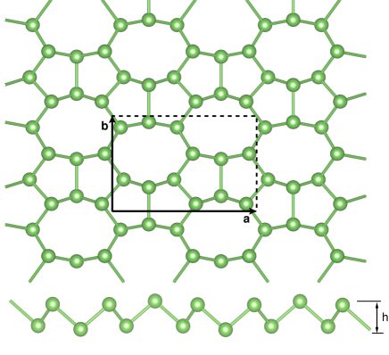
The crystal structure of a typical pentaoctite sheet is shown in Fig. 1. The top view shows that the new phase is composed of two side-sharing pentagons connected to octagon rings. The unit cell contains 12 atoms. The side view (lower panel) shows the buckling height (h). Typically, the nearest-neighboring atoms belong to different sublayers. The equilibrium in-plane parameters of pentaoctite sheet of P, As, and Sb are =9.00 Å, =6.33 Å; =9.76 Å, =7.05 Å and = 11.07 Å, = 8.00 Å, respectively. Buckling increases with atomic number and is larger for Sb. These lattice parameters increase as the atomic size increases. The optimized structural parameters are shown in Table 1.
[figure]style=plain,subcapbesideposition=top
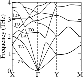
In order to study the stability of pentaoctite sheets of P, As, and Sb, we examined the phonon dispersions along the high-symmetry lines in the Brillouin zone (BZ) (Fig. 2). No imaginary modes are present, confirming that the freestanding pentaoctite sheet is dynamically stable. Similarly to other 2D layered materials Wang et al. (2016b); Zhang et al. (2015b), there are three distinct acoustic modes in the phonons spectra of pentactite. The in-plane longitudinal acoustic (LA) and transverse acoustic branches (TA) have linear dispersions near the point, whereas the out-of-plane acoustical modes (ZA) has quadratic dispersion. The quadratic ZA mode in the long-wavelength region is closely associated with the bending rigidity and lattice heat capacity of the nanosheets, as discussed in pentagraphene Zhang et al. (2015a) Also, there is a hybridization of ZA and ZO modes in all phonon dispersions. As a matter of comparison, in hexagonal As, the optic and acoustic branches are well separated by a gap Rahman et al. (2019). Although the presence of imaginary frequencies is not seen, the parabolic behavior of one of the acustic modes close to the -point is present Fig. 2. In general, the ZA mode is very soft in 2D materials, and a slight reduction of the lattice constant may result in imaginary phonon frequencies near the point. In particular for pentaoctite phophosrene this behavior is more emphasized, as shown in Fig. 2 (c).
[] \sidesubfloat[]
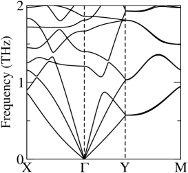 \sidesubfloat[]
Additionally we have calculated the energy formation of pentaoctite sheets, E, with respect to the honeycomb structures. The formation energy is defined as ,where Etotal is the total energy of pentactite (P, As, and Sb), Natom is the total number of atoms in the crystal structure, and is the energy per atom calculated for hexagonal honeycomb structure. The relative formation energies of pentaoctite sheets of P, As, and Sb are 46 meV/atom, 49 meV/atom, and 62 meV/atom, respectively.
[]
\sidesubfloat[]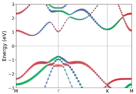
\sidesubfloat[]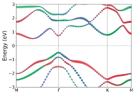
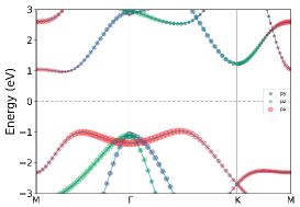
In order to compare the band structures of hexagonal and pentaoctite structures, we have calculated the orbital projected band structure of hexagonal blue phosphorene, arsenene and atimonene. These are shown in Fig. 3. Hexagonal blue phosphorene is a indirect band gap semiconductor with the conduction band minimum (CBM) located between the and M points while valence band maximum (VBM) is located between the K and points, as seen in Fig. 3(a). Most contribution at VBM comes from px orbitals. Band gap is around 1.91 eV, in good agreement with previous GGA investigations Ospina et al. (2016); Peng et al. (2016). The band gap of pentaoctite-P is around 1.01 eV (1.34 eV with HSE). These values are reported in Table 1. Buckled hexagonal arsenene is an indirect bandgap semiconductor with the VBM at the -point and the CBM along the -M-direction, as shown in Fig. 3(b). The calculated indirect band gap is 1.53 eV in agreement with previous calculations Jamdagni et al. (2018). HSE indirect has been reported to be 2.89 Rahman et al. (2019). Furthermore a free standing monolayer of hexagonal As has negative frequencies and therefore though the structure is energetically stable, it is dynamically not stable Rahman et al. (2019); Kamal and Ezawa (2015). On the other hand, our results show that the calculated band gaps of pentaoctite-As are 1.13 eV with GGA and 1.36 eV with HSE, as shown in Table 1.
[] \sidesubfloat[]
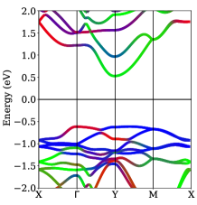 \sidesubfloat[]
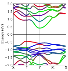
\sidesubfloat[]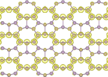 \sidesubfloat[]
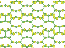 \sidesubfloat[]
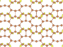
In hexagonal Sb, VBM is at -point and CBM between and M points as seen in Fig. 3 (c). Hexagonal antimonene has a band gap of 1.02 in good agreement with other calculations Zhang et al. (2016); Singh et al. (2016). Finally in pentaoctite-Sb Kecik et al. (2018) the energy fundamental band gap is 0.83 eV with GGA and 1.01 eV with HSE as seen in Table 1. As a general conclusion, the band gaps in pentaoctite phases are larger than in hexagonal phases for P, As and Sb. This difference in the band structure and band character can be understood considering the different buckling and hybridization.
Fig.4 the band decomposed charge density at VBM for pentaoctite phases of P, As and Sb at zero strain. One can see that for P, Fig.4 (d) the main contribution comes from orbitals pz. For As, as shown in Fig.4 (e), the main contribution comes from orbitals px. Finally, for Sb the main contribution comes from orbitals px as seen in Fig. 4 (f). The flatening of the band structure is due to the different hybridization within the octagon-pentagon rings, as discussed in Ref. Lima et al. (2019, 2016).
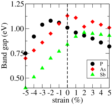
It is known that external strain can be used to tune and modify the electronic band structure of materials. As all investigated structures show indirect band in the pentaoctite phase. Therefore we have applied compressive and tensile strains between -5% and +5%. Fig. 5 shows that indeed the band gap is sentisive to strain. However, all structure are more sensitive to negative (compressive) strain than to positive (tensile) strain. In particular, pentaoctite-As shows the largest variation for tensile strain.
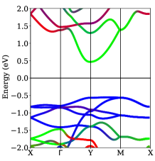
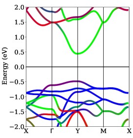
The resulting band structures of strained pentaoctites are shown in Fig. 6. The specific strain show the transition from indirect to direct bandgap with a VBM and CBM at the Y point. In pentaoctite-P compressive strains 4% (Figs. 6 (a)) leads to a direct bandgap, whereas tensile strains 5% transform pentaoctite-As and pentaoctite-Sb (Figs. 6 (b) and (c)) into a direct bandgap semiconductor.
[] \sidesubfloat[]
 \sidesubfloat[]
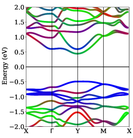
 |
 |
 |
 |
It has been predicted that several two-dimensional materials behave like topological insulators, which implies the presence of conducting edge states carrying two counter-propagating spin-polarized currents Kane (2013). Due to constraints of time-reversal symmetry, these conducting edge states are protected against backscattering, making them suitable for spintronics applications. Although graphene was initially proposed behave like a topological insulator, the spin-orbit coupling (SOC) in this material is very weak. In group V-materials, hexagonal and pentaoctite bismuth monolayers have been predicted to be a 2D topological insulator (TI) Kou:NL; Freitas et al. (2015); Song et al. (2014); Reis et al. (2017); da Rosa et al. ; Lima et al. (2019, 2016). In order to investigate whether the pentaoctite sructures behave like topological insulators we have calculated the Z2 invariant according to Ref. Kane (2013). On the contrary of pentaoctite bismuthene, our investigated structures are not topological insulators.
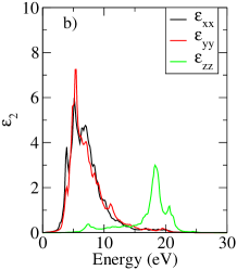
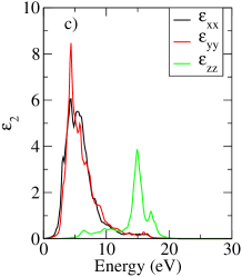
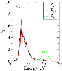
Finally, the dielectric function of pentaoctite layers were investigated by calculating the imaginary part of the dielectric function at G level. This means that the Green’s functions are calculated iteratively whereas the Coulomb potential W is kept at the DFT level. The imaginary part of the dielectric function is calculated directly from the electronic structure through the joint density of states and the momentum matrix elements occupied and unoccupied eigenstates according Ref.Shishkin et al. (2007).
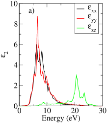
We show the dielectric function calculated within the G approximation in Fig. 7. The parallel and and perpendicular components of the the imaginary part of the dielectric function are shown. The parallel components corresponds to the propagation of the external electromagnetic field parallel to the pentaoctite plane while corresponds to the field perpendicular to the plane. Because of optical selection rules, anisotropy in the optical spectra is seen. Anisotropy has also been reported in layered monochalcogenide of germanium sulfide (GeS) Research (2017), black phosphorous Rudenko et al. (2015) and bismutheneKecik et al. (2018); da Rosa et al. and germanene de Oliveira et al. (2020). The systems with a gap show finite absorption limits for both parallel and perpendicular directions with larger intensity for the component.
In the imaginary part of the dielectric function, the energy onsets are 2.6 as seen in Fig. 7(a), 2.1 seen in Fig. 7(b) and 1.51 eV seen in Fig. 7(a) for P, As and Sb, respectively. Additionally, there are only one main peak around 7.0, 5.27 and 6.2 eV for P, As and Sb, respectively. Materials with band gaps below the 1.65 eV absorb well in the infrared (IR) region of the spectrum. Therefore, antimonene will start to absorb electromagnetic radiation in the IR region as an optical material, but absorption in antimonene will be strongest in the UV part of electromagnetic spectrum. In Fig. 7(d) we show the dielectric function for strained antimonene. The strain shifts the spectrum to smaller energies, as expected.
IV Conclusions
We have performed density-functional theory calculations for group V allloropes. We show that pentactotie structures of these materials are stable. The electronic properties show a sizeable band gap with absorption spectrum in the visible region. We suggested that such defects can be useful as building blocks for group-V electronics.
V Acknowledgements
We acknowledge the financial support from the Brazilian Agency CNPq and FAPEG (PRONEX 201710267000503) and German Science Foundation (DFG) under the program FOR1616. The calculations have been performed using the computational facilities of Supercomputer Santos Dumont and at QM3 cluster at the Bremen Center for Computational Materials Science and CENAPAD.
References
- Geim and Novoselov (2007) A. K. Geim and K. S. Novoselov, Nature Materials 6, 183 (2007).
- Novoselov et al. (2004) K. Novoselov, A. Geim, S. Morozov, D. Jiang, Y. Zhang, S. Dubonos, I. Grigorieva, and A. F. rsov, Science 306, 666 (2004).
- da Silva-Araujo et al. (2010) J. da Silva-Araujo, H. Chacham, and R. W. Nunes, Phys. Rev. B (2010), https://doi.org/10.1103/PhysRevB.81.193405.
- da Silva-Araujo et al. (2012) J. da Silva-Araujo, A. J. M. Nascimento, H. Chacham, and R. W. Nunes, Nanotechnology 24, 035708 (2012).
- Alexandre et al. (2012) S. S. Alexandre, A. D. Lucio, A. H. C. Neto, and R. W. Nunes, Nano Lett. 12, 5097 (2012).
- Zhang et al. (2015a) S. Zhang, J. Zhou, Q. Wang, X. Chen, Y. Kawazoe, and P. Jena, PNAS 112, 2372 (2015a).
- dos Santos et al. (2020) R. M. dos Santos, L. E. de Sousa, D. S. G. ao, and L. A. Ribeiro, Sci. rep. , 8014 (2020).
- Chen et al. (2014) J.-H. Chen, G. Auès, N. Alem, F. Gargiulo, A. Gautam, M. Linck, C. Kisielowski, O. V. Yazyev, S. G. Louie, and A. Zettl, Phys. Rev. B 89, 121407(R) (2014).
- Lahiri et al. (2010) J. Lahiri, Y. Lin, P. Bozkurt, I. I. Oleynik, and M. Batzill, Nat. Nanotechnol. 5, 326 (2010).
- Lima et al. (2019) E. N. Lima, T. M. Schmidt, and R. W. Nunes, J. Phys.: Condens. Matter 31, 475001 (2019).
- Lima et al. (2016) E. N. Lima, T. M. Schmidt, and R. W. Nunes, Nano Lett. (2016).
- Yang et al. (2017) G. Yang, Z. X., Z. L., S. Jin, H. Zhang, and Z. Ding, J. Phys. Chem. C 121, 12945 (2017).
- Rahman et al. (2019) G. Rahman, A. Mahmood, and V. M. Garcia-Suarez, Sci. Rep. 9, 7966 (2019).
- Wang et al. (2016a) Y.-P. Wang, W.-X. Ji, C.-W. Zhang, P. Li, F. Li, M.-J. Ren, X.-L. C. M. Y., and P.-J. Wang, Sci. Rep. 6, 20342 (2016a).
- Chuang et al. (2013) F.-C. Chuang, C.-H. Hsu, C.-Y. Chen, Z.-Q. Huang, V. Ozolins, H. Lin, and A. Bansil, Appl. Phys. Lett. 102, 022424 (2013); 102, 022424 (2013).
- Zhu et al. (2019) S.-Y. Zhu, Y. Shao, E. Wang, L. Cao, X.-Y. Li, Z.-L. Liu, C. Liu, L.-W. Liu, J.-O. Wang, K. Ibrahim, J.-T. Sun, Y.-L. Wang, S. Du, and H.-J. Gao, Nano Lett. 19, 6323 (2019).
- Hohenberg and Kohn (1964) P. Hohenberg and W. Kohn, Phys. Rev. 136, B864 (1964).
- Kohn and Sham (1965) W. Kohn and L. J. Sham, Phys. Rev. 140, A1133 (1965).
- Kresse and Furthmüller (1996) G. Kresse and J. Furthmüller, Phys. Rev. B 54, 11169 (1996).
- Perdew et al. (1996) J. P. Perdew, K. Burke, and M. Ernzerhof, Phys. Rev. Lett. 77, 3865 (1996).
- Blöchl (1994) P. E. Blöchl, Phys. Rev. B 50, 17953 (1994).
- Kresse and Joubert (1999) G. Kresse and D. Joubert, Phys. Rev. B 59, 1758 (1999).
- Monkhorst and Pack (1976) H. J. Monkhorst and J. D. Pack, Phys. Rev. B 13, 5188 (1976).
- Togo and Tanaka (2015) A. Togo and I. Tanaka, Scr. Mater. , 1 (2015).
- Shishkin et al. (2007) M. Shishkin, M. Marsman, and G. Kresse, Phys. Rev. Lett. 99, 246403 (2007).
- Wang et al. (2016b) Z. Wang, F. Dong, B. Shen, R. Zhang, Y. Zheng, L. Chen, S. Wang, C. Wang, K. Ho, Y.-J. Fan, B.-Y. Jin, and W.-S. Su, Carbon 101, 77 (2016b).
- Zhang et al. (2015b) S. Zhang, J. Zhou, Q. Wang, X. Chen, Y. Kawazoe, and P. Jena, Proceedings of the National Academy of Sciences 112, 2372 (2015b), https://www.pnas.org/content/112/8/2372.full.pdf .
- Ospina et al. (2016) D. A. Ospina, C. A. Duque, J. Corre, and E. S. Morell, Superlattices and Microstructures , 562 (2016).
- Peng et al. (2016) Q. Peng, Z. Wang, B. Sa, B. Wu, and Z. Sun, Sci. Rep. 6, 31994 (2016).
- Jamdagni et al. (2018) P. Jamdagni, A. Thakur, A. Kumar, P. K. Ahluwalia, and R. Pandey, Phys. Chem. Chem. Phys. (2018), https://doi.org/10.1039/C8CP06162A.
- Kamal and Ezawa (2015) C. Kamal and M. Ezawa, Phys. Rev. B 91, 085423 (2015).
- Zhang et al. (2016) S. Zhang, M. Xie, F. Li, Z. Yan, Y. Li, E. Kan, W. Liu, Z. Chen, and H. Zeng, Angew. Chem. 128, 1698 (2016).
- Singh et al. (2016) D. Singh, S. K. Gupta, Y. Sonvane, and I. Lukacevic, J. Mater. Chem. C (2016), https://doi.org/10.1039/C6TC01913G.
- Kecik et al. (2018) D. Kecik, V. O. Özçlik, E. Durgun, and S. Ciraci, Phys. Chem. Chem. Phys. 21, 7907 (2018).
- Kane (2013) C. L. Kane, Contemporary Concepts of Condensed Matter Science 6, 3 (2013).
- Freitas et al. (2015) R. R. Q. Freitas, R. Rivelino, F. de Brito Mota, C. M. C. de Castilho, A. Kakanakova-Georgieva, and G. K. Gueorguiev, JPCC 119, 23599 (2015).
- Song et al. (2014) Z. Song, C.-C. Liu, J. Yang, J. Han, M. Ye, B. Fu, Y. Yang, Q. Niu, J. Lu, and Y. Yao, NPG Asia Materials 6, e147 (2014).
- Reis et al. (2017) F. Reis, G. Li, L. Dudy, M. Bauernfeind, Glass, W. Hanke, R. Thomale, J. Schäfer, and R. Claessen, Science , 10.1126/science.aai8142 (2017).
- (39) A. L. da Rosa, E. N. Lima, M. C. da Silva, R. B. Pontes, J. S. de Almeida, T. M. Schmidt, and T. Frauenheim, , 11708.
- Research (2017) N. Research, Nano Research , 546 (2017).
- Rudenko et al. (2015) A. Rudenko, S. Yuan, and M. Katsnelson, Phys. Rev. B 92, 085419 (2015).
- de Oliveira et al. (2020) F. B. de Oliveira, A. L. Rosa, E. N. Lima, M. C. da Silva, , and T. Frauenheim, Phys. Chem. Chem. Phys. (2020), accepted.