Metasurface retroreflector for controlling parasitic surface waves on bodies of 5G mobile phones
Abstract
The smartphone, as a media device, should offer a large-size screen and fast data rates in a well-packed device. Emergent 5G technologies based on millimeter waves need efficiently radiating antennas integrated into devices whose bodies (especially glass screens) behave as waveguides in the antenna frequency bands. Using the concept of retroreflective surfaces, this work proposes a compact metasurface located below the smartphone glass screen which reduces surface-wave excitation and propagation, and significantly improves the radiation pattern and efficiency of millimeter-wave antennas integrated into mobile terminals.
Index Terms:
Millimeter wave, mobile phone antenna, 5G, surface waves, retroreflector, metasurfaceI Introduction
From watching a video to writing a scientific article, the smartphone has become the 21st century Swiss Army knife: compact yet versatile. As a streaming device, the smartphone requires high-speed communication solutions. It is expected that 5G technologies in the millimeter-wave (mmWave) range GHz ( mm) [1, 2, 3, 4] could grant transfer rates in the order of Gbps [5, 6, 7]. However, practical implementation becomes troublesome as the wavelength is smaller than the device dimensions.

In order to achieve a wide-beam full-sphere coverage and minimize user blockage, one of the following designs of a mobile device can be used: three end-fire antenna array modules on the top, left and right sides, respectively; or two antenna arrays at the front and back sides, respectively. It was shown in [8, 9] that both designs have comparable performance in terms of beamforming antenna gain patterns and link budgets, and robust performance with hand blockage. Implementation of end-fire antennas is limiting the display size and display edge curvature of the mobile device. Preferable edge areas with statistically less impact of the hand blockage are the same for the end-fire mmWave array modules and for sub-6 GHz antennas. Positioning of mmWave end-fire antenna array modules impose limitations on the space available for sub-6 GHz antennas. Therefore, display-side and backside mmWave antenna array modules are beneficial from the full-screen design and multiband wireless connectivity considerations.
In conceptual studies of device-integrated millimeter-wave antennas, a smartphone can be considered as a multilayered structure consisting of a glass layer, a dielectric layer (which combines the tactile panel and the screen display) with some effective permittivity, over a metallic chassis. A 5G antenna located under the glass, as shown in Fig. 1, would excite surface waves along the glass and dielectric layers, as in a dielectric-slab waveguide. The dispersion properties of surface waves, both TE- and TM-polarized modes, can be deduced analytically using the vector transmission-line method [10]. The dispersion equations for TE- and TM-modes read, respectively,
| (1a) | ||||
| (1b) | ||||
| (1c) | ||||
| (1d) | ||||
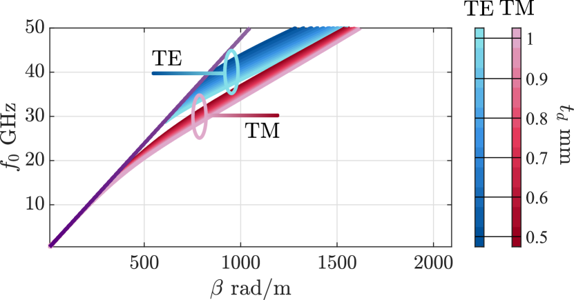
where and are the glass thickness and relative permittivity, respectively, while and are the respective parameters for the dielectric layer. The dispersion diagram of Fig. 2 shows that, with the typical dimensions of commercial smartphones, an antenna behind the glass can excite TM waves at the frequencies as low as 20 GHz, while TE modes propagate starting from approximately 30 GHz.
Surface wave excitation distorts the desired radiation pattern, compromising scattering along the multi-layer plane. Moreover, the presence of the glass and dielectric layers produces mismatch between the 5G antenna and the free space, which decreases the overall efficiency. In practical terms, the waveguide supported by the reinforced glass covers at the front and back sides of the mobile device results in additional dissipative loss of 1–3 dB [11, 12]. Mobile device antennas utilize various techniques for controlling current distribution on the ground plane, such as a parasitic inverted L-antenna (ILA) element located at the ground edge [13] or wavetraps at the antenna connection to the ground plane [14].
It shall be noted that typically surface wave suppression is used for improvement of isolation between adjacent antennas, and currents on the ground plane edges are suppressed by electromagnetic bandgap (EBG) unit cells [15]. From the analysis of different approaches, found in the literature [16, 17, 18, 19, 20, 21], it is clear that volumetric, 3D unit cells cannot be easily implemented inside dielectric layers; while a flat structure, more friendly in terms of implementation, can be capable of directing electromagnetic waves away from the surface. It is important that these planar structures can be designed to remain practically invisible to the human eye [22, 23], as the solution must not affect display visibility. Moreover, a compact structure will reduce potential electromagnetic compatibility issues.
We expect that recently conceptualized metasurface retroreflectors [24, 25, 26], which are capable of reflecting an incident wave back along the illumination direction, can be a valuable solution. For this application, it is expected that a retroreflecting metasurface can work as a decoupling structure between the antenna and the layered body of the device, sending the waves created by the antenna back into space (primarily along the incidence direction and with a controllable reflection phase) and contributing to better radiation performance. In contrast to conventional stop-band solutions discussed above, the propagation of the surface wave is not suppressed. Instead, these waves are re-radiated into space, preferably along the desired direction. These retroreflective devices can be implemented designing metasurfaces which ensure the desired phase matching between the incident and reflected waves [27, 28, 29, 30].
In this paper, we present a solution based on the use of retroreflective metasurfaces, which allows us to minimize the propagation of surface waves across an all-screen device in the mmWave regime, when the antenna is placed behind the glass, close to the screen edge. The paper is organized as following: First, we introduce the retroreflector solution and explain its operation principle, and then present the methodology and design results. In the results section, the performance of the retroreflective surface is validated using full-wave simulations.
II Retroreflectors for surface wave control
II-A Surface Impedance
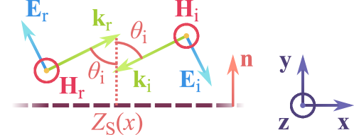
A retroreflective surface can be characterized by its surface (input) impedance that relates the total (incident plus reflected) tangential electric and magnetic fields at its surface:
| (2) |
where is the unit vector normal to the surface [10]. The retroreflector is designed for TM-polarized waves, because surface waves of TE polarization can propagate through the device only above 30 GHz, see Fig. 2. Using the representation of a TM-retroreflector of Fig. 3, the incident and reflected waves are written, respectively, as
| (3a) | ||||
| (3b) | ||||
| (4a) | ||||
| (4b) | ||||
where is the reflection coefficient, is the incidence angle, and is the wave impedance of the medium above the retroreflective surface. The corresponding total tangential magnetic and electric fields, required to define , are the sums of the incident and reflected fields at the interface ():
| (5a) | ||||
| (5b) | ||||
The surface impedance for a retroreflective surface reads
| (6) |
where is the phase gradient required for the proper operation of the metasurface. In case of total retroreflection (), the surface impedance is reduced to
| (7) |
These results show that the retroreflective surface is a lossless periodic structure (with the period ) and strongly frequency and incidence-angle dependent. The period increases when the incidence angle decreases, and in the limit of zero angle (normal incidence), the retroreflector degenerates to a usual uniform mirror.
II-B Grid Impedance
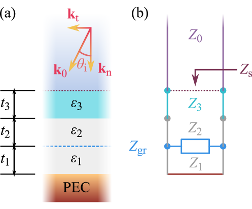
In the previous subsection, we modeled the retroreflector as an idealized surface impedance boundary. In practice, the retroreflector can be realized as a multilayer structure consisting of two dielectric layers and a structured metal film placed in the middle of the second layer, as shown in Fig. 4(a). The structure should be designed to produce a virtual retroreflector at the top glass surface, as explained in the equivalent system circuit in Fig. 4(b), where the input impedance at the top of the glass layer is equal to the retroreflector surface impedance. The structured metal film can be viewed as a single-layer metasurface, which can be characterized by a grid impedance that defines a discontinuity of the total tangential magnetic field at the metasurface plane.
| (8) |
Using the transmission-line theory [31], we can calculate the input impedance of the multilayer system and equate it to the required surface impedance of a retroreflective surface , as shown in Fig. 4. Each dielectric layer behaves as a transmission line, with the corresponding TM characteristic impedance and equivalent propagation constant [10]. After equating the input impedance of the multilayer system with the retroreflector surface impedance, the required grid impedance can be written as in Eq. (8), where and with representing the three dielectric layers.
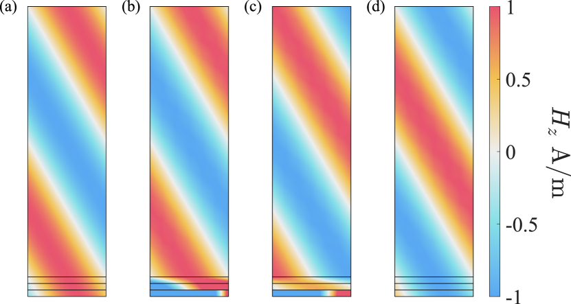
To verify Eq. (8), we use a Comsol model (Fig. 4) with the following parameters: mm, , , , GHz. The results of the simulation show that the incident [Fig. 5(a)] and reflected [Figs. 5(b)–(d)] magnetic fields propagate in the opposite directions, as desired. It is also important to mention tunability of the reflection phase, as it is illustrated in Figs. 5(b)–(d). This parameter will take an important role in the design of the metasurface for surface waves decoupling.
II-C Discretization tolerance
In the previous subsection, we considered a continuously varying grid impedance [see the blue curve in Fig. 6(b)], which is not possible to implement in practice, because unit cells have finite sizes. To solve this issue, the grid impedance should be discretized to a finite set of points [32]. An example of a discretized impedance is shown in Fig. 6(b) (orange points).
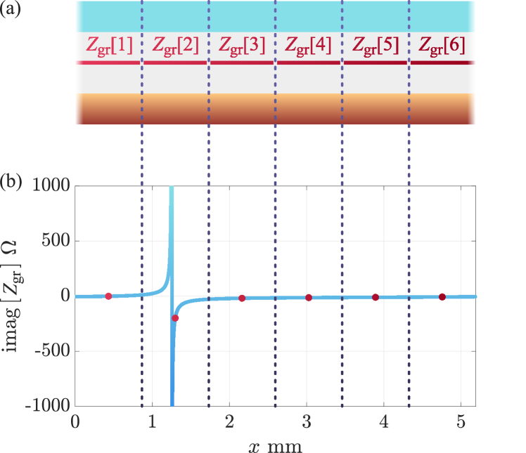
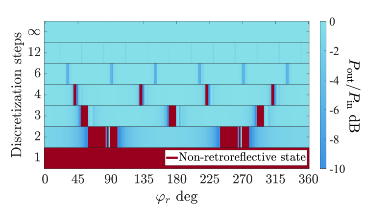
The performance of the discretized metasurface will be affected by the number of discretization steps, as shown in Fig. 7. As expected, it is not possible to achieve retroreflection using a single discretization step, as the resulting structure does not compensate the incidence wave phase, and it behaves as a conventional specular reflector. However, as the number of discretization steps increases, the metasurface can be tuned to achieve retroreflection with acceptable performance. Based on the information provided in Fig. 7, using six discretization steps offers a good trade-off between performance for almost every value of (required for fine tuning) and number of required different impedance values.
III Metasurface implementation
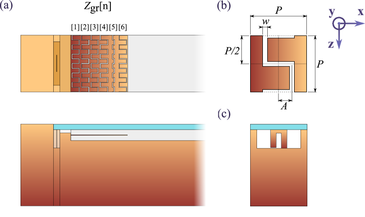
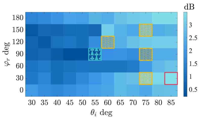
The performance of the proposed retroreflective sheet is evaluated in the structure shown in Fig. 8, where a folded dipole excites parasitic surface waves along the dielectric and glass layers. The retroreflective metasurface is located in the middle of the dielectric layer, aligned with a metallic wall that prevents wave propagation below the metasurface. Using six discretization sub-cells, the optimal values for and were found using numerical (CST) simulations. The used optimization criterion was the maximized radiation in the -direction with the beamwidth of , compared to the performance in the same range without the retroreflector. The retroreflective layer was tested for different values of in the range between and using steps; in combination with values of in the range between and with steps. The simulation results for each combination of and are collected in Fig. 9. Due to numerical singularities, some parameter combinations could not be tested reliably, and we display the averaged values using instead. Nevertheless, these estimated values are far away from the optimal region of interest, close to . As a result, the optimal performance using ideal discretized surface impedances was found with and .
Due to its capacitive nature, the retroreflective metasurface can be realized using the meandered-slot topology [27], illustrated in Fig. 8(b). While the period of the meandered-slot unit cell is fixed to be one sixth of the grid impedance period , the other parameters (the gap width and the meander amplitude ) had to be tuned for every sub-cell to achieve the required reactance. The designed values are collected in Table I.
| Subcell | 1 | 2 | 3 | 4 | 5 | 6 |
|---|---|---|---|---|---|---|
| -47 | -254 | -68 | -62 | -58 | -55 | |
| 60 | -1255 | -54 | -18 | 0.86 | 20 | |
| mm | 0.34 | 0.26 | 0.34 | 0.32 | 0.34 | 0.33 |
| mm | 0.06 | 0.065 | 0.065 | 0.055 | 0.063 | 0.058 |
IV Results
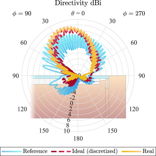
The efficiency of the proposed solution can be estimated by comparing the device shown in Fig. 8 with and without the retroreflective metasurface. Figure 10 contrasts the far-field directivity of the reference antenna, that with the ideal discretized metasurface, and with its meandered-slot implementation at the reference frequency of 29 GHz. The use of the retroreflective sheet decreases the radiation along the multilayered structure plane, while the directivity is improved in the direction normal to the layers, as desired. Small optimizations of each sub-cell parameter allows us to maintain and improve the resulting radiation pattern.
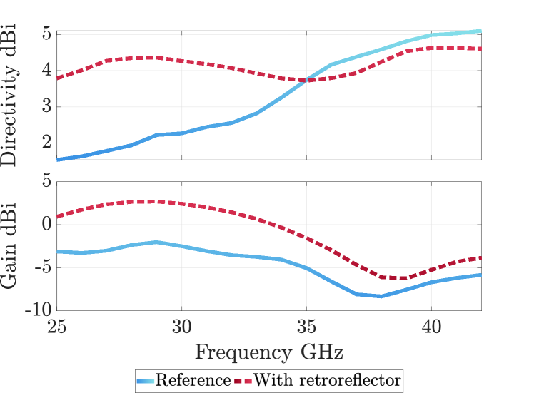
As a complement, Fig. 11 offers a deeper insight on how the retroreflective layer performs across the frequency range of 25–42 GHz. The capacitive, non-resonant nature of the retroreflector grants a broadband frequency response in terms of the average directivity (around 4 dBi), outperforming the out-of-the-box device for frequencies lower than 35 GHz, while for higher frequencies the performance is similar. In terms of gain, Fig. 11 proves that a retroreflective layer can improve the performance of a 5G device, with a gain improvement oscillating between 1.3 and 5.4 dB.
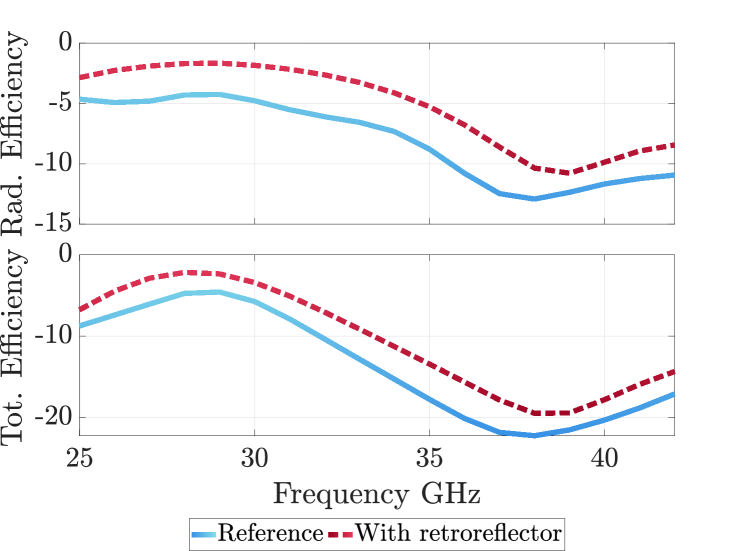
In terms of radiated power, Fig. 12 shows that the combined antenna-retroreflector systems are capable to radiate power more efficiently. The radiation efficiency, without considering antenna impedance matching, increases by 1.57–4.01 dB by using a retroreflector. Similar results can be observed for the total efficiency, including impedance matching, where the retroreflector improves the performance by 1.99–4.47 dB.
V Conclusions
In this work we have introduced a retroreflective surface capable to improve the radiation pattern and efficiency of smartphone antennas in the mmWave frequency range. By using the concept of retroreflection, a metasurface was designed to create a virtual retroreflective surface over the glass surface, with adjustable reflection phase. The resulting grid impedance matches the TM-polarized wave inside the dielectric layer, reducing the parasitic wave propagating along the smartphone body. The retroreflecting element prevents parasitic channeling of the antenna energy into surface waves in and behind the glass layer and directs the radiation into the desired direction, in contrast to conventional periodical stop-band structures that only forbid propagation of surface waves.
The discretization of the impedance profile, required for a plausible realization, was realized as a trade-off between performance and complexity with a sweet spot of six sub-cells. The phase of the retroreflected wave became a relevant parameter for fine tuning and for choosing a favourable set of grid impedance values. A topology based on meandered slot unit-cells was selected due to the pure capacitive nature of the required grid impedance.
To achieve a compact design, the resulting metasurface only covers one period of the surface impedance, without compromising performance. The proposed structure shows improvements in radiative and efficiency terms, granting improvements in antenna directivity and gain around 2 dB and 5 dB, respectively; while the antenna efficiency increases around 4 dB. The non-resonant nature of the metasurface allows improvement of the antenna performance in a wide frequency range.
References
- [1] V. Viikari, J. Ala-Laurinaho, J. Kurvinen, H. Kahkonen, A. Lehtovuori, M. Leino, and Z. N. Chen, “Millimeter-wave antennas for mobile devices and networks,” in 2019 12th Global Symposium on Millimeter Waves (GSMM). IEEE, may 2019.
- [2] Z. Yong, “A transparent dual-band dual-polarized mm-wave antenna array for 5g smartphone application,” in 2019 International Symposium on Antennas and Propagation (ISAP), 2019, pp. 1–3.
- [3] Y. He, M. Rao, Y. Liu, G. Jing, M. Xi, and L. Zhao, “28/39-GHz dual-band dual-polarized millimeter wave stacked patch antenna array for 5g applications,” in 2020 International Workshop on Antenna Technology (iWAT). IEEE, feb 2020.
- [4] M. Ikram, N. Nguyen-Trong, and A. Abbosh, “Hybrid antenna using open-ended slot for integrated 4g/5g mobile application,” IEEE Antennas and Wireless Propagation Letters, vol. 19, no. 4, pp. 710–714, apr 2020.
- [5] M. A. M. Albreem, “5g wireless communication systems: Vision and challenges,” in 2015 International Conference on Computer, Communications, and Control Technology (I4CT). IEEE, apr 2015.
- [6] Y. Qi, M. Hunukumbure, M. Nekovee, J. Lorca, and V. Sgardoni, “Quantifying data rate and bandwidth requirements for immersive 5g experience,” in 2016 IEEE International Conference on Communications Workshops (ICC). IEEE, may 2016.
- [7] X. Lu, M. Lema, T. Mahmoodi, and M. Dohler, “Downlink data rate analysis of 5g-u (5g on unlicensed band): Coexistence for 3gpp 5g and ieee802. 11ad wigig,” in European Wireless 2017; 23th European Wireless Conference. VDE, 2017, pp. 1–6.
- [8] V. Raghavan, M.-L. Chi, M. A. Tassoudji, O. H. Koymen, and J. Li, “Antenna placement and performance tradeoffs with hand blockage in millimeter wave systems,” IEEE Transactions on Communications, vol. 67, no. 4, pp. 3082–3096, apr 2019.
- [9] A. Hazmi, R. Tian, S. Rintamaki, Z. Milosavljevic, J. Ilvonen, J. van Wonterghem, A. Khripkov, and T. Kamyshev, “Spherical coverage characterization of millimeter wave antenna arrays in 5g mobile terminals,” in 2019 13th European Conference on Antennas and Propagation (EuCAP), 2019, pp. 1–5.
- [10] S. Tretyakov, Analytical Modeling in Applied Electromagnetics. Artech House In, 2003.
- [11] I. Syrytsin, S. Zhang, G. F. Pedersen, K. Zhao, T. Bolin, and Z. Ying, “Statistical investigation of the user effects on mobile terminal antennas for 5g applications,” IEEE Transactions on Antennas and Propagation, vol. 65, no. 12, pp. 6596–6605, dec 2017.
- [12] Qualcomm, “R4-1800369, on UE packaging loss, simulation results,” in 3GPP TSG-RAN WG4 Meeting AH-1801, Jan 2018.
- [13] M. R. Islam and M. Ali, “Ground current modification of mobile terminal antennas and its effects,” IEEE Antennas and Wireless Propagation Letters, vol. 10, pp. 438–441, 2011.
- [14] Z. Ying and K. Zhao, “Dual-band inverted-f antenna with multiple wave traps for wireless electronic devices,” U.S. Patent US9 819 086B2, Nov. 14, 2017.
- [15] J. Lee, S. Jung, Y. Youn, J. Park, W. Kwon, and W. Hong, “Optically transparent 1-d ebg antenna using sub-skin depth thin-film alloy in the ka-band,” in 2019 13th European Conference on Antennas and Propagation (EuCAP), 2019, pp. 1–3.
- [16] P.-S. Kildal, “Artificially soft and hard surfaces in electromagnetics,” IEEE Transactions on Antennas and Propagation, vol. 38, no. 10, pp. 1537–1544, 1990.
- [17] D. Sievenpiper, L. Zhang, R. Broas, N. Alexopolous, and E. Yablonovitch, “High-impedance electromagnetic surfaces with a forbidden frequency band,” IEEE Transactions on Microwave Theory and Techniques, vol. 47, no. 11, pp. 2059–2074, 1999.
- [18] B.-I. Wu, H. Chen, J. A. Kong, and T. M. Grzegorczyk, “Surface wave suppression in antenna systems using magnetic metamaterial,” Journal of Applied Physics, vol. 101, no. 11, p. 114913, jun 2007.
- [19] C. Mulenga and J. Flint, “Planar electromagnetic bandgap structures based on polar curves and mapping functions,” IEEE Transactions on Antennas and Propagation, vol. 58, no. 3, pp. 790–797, mar 2010.
- [20] A. Kumar, J. Mohan, and H. Gupta, “Surface wave suppression of microstrip antenna using different EBG designs,” in 2015 International Conference on Signal Processing and Communication (ICSC). IEEE, mar 2015.
- [21] H. Oraizi, A. Amini, A. Abdolali, and A. M. Karimimehr, “Design of wideband leaky-wave antenna using sinusoidally modulated impedance surface based on the holography theory,” IEEE Antennas and Wireless Propagation Letters, vol. 17, no. 10, pp. 1807–1811, oct 2018.
- [22] J. Park, S. Y. Lee, J. Kim, D. Park, W. Choi, and W. Hong, “An optically invisible antenna-on-display concept for millimeter-wave 5g cellular devices,” IEEE Transactions on Antennas and Propagation, vol. 67, no. 5, pp. 2942–2952, may 2019.
- [23] M. Stanley, Y. Huang, H. Wang, H. Zhou, A. Alieldin, and S. Joseph, “A transparent dual-polarized antenna array for 5g smartphone applications,” in 2018 IEEE International Symposium on Antennas and Propagation & USNC/URSI National Radio Science Meeting. IEEE, jul 2018.
- [24] V. Asadchy, A. Díaz-Rubio, S. Tcvetkova, D.-H. Kwon, A. Elsakka, M. Albooyeh, and S. Tretyakov, “Flat engineered multichannel reflectors,” Physical Review X, vol. 7, p. 031046, 2017.
- [25] C. Shen, A. Díaz-Rubio, J. Li, and S. A. Cummer, “A surface impedance-based three-channel acoustic metasurface retroreflector,” Applied Physics Letters, vol. 112, no. 18, p. 183503, apr 2018.
- [26] G. Y. Song, Q. Cheng, T. J. Cui, and Y. Jing, “Acoustic planar surface retroreflector,” Physical Review Materials, vol. 2, no. 6, jun 2018.
- [27] X. Wang, A. Díaz-Rubio, V. S. Asadchy, G. Ptitcyn, A. A. Generalov, J. Ala-Laurinaho, and S. A. Tretyakov, “Extreme asymmetry in metasurfaces via evanescent fields engineering: Angular-asymmetric absorption,” Physical Review Letters, vol. 121, no. 25, dec 2018.
- [28] T. Nagayama, S. Fukushima, A. Sanada, and T. Watanabe, “Flat retroreflector based on transformation electromagnetics,” in 2016 International Conference on Advanced Technologies for Communications (ATC). IEEE, oct 2016.
- [29] A. Arbabi, E. Arbabi, Y. Horie, S. M. Kamali, and A. Faraon, “Planar metasurface retroreflector,” Nature Photonics, vol. 11, no. 7, pp. 415–420, jun 2017.
- [30] L. Yan, W. Zhu, M. F. Karim, H. Cai, A. Y. Gu, Z. Shen, P. H. J. Chong, D.-L. Kwong, C.-W. Qiu, and A. Q. Liu, “0.2 thick adaptive retroreflector made of spin-locked metasurface,” Advanced Materials, vol. 30, no. 39, p. 1802721, aug 2018.
- [31] F. T. Ulaby, Fundamentals of Applied Electromagnetics, 5th ed. Prentice Hall, 2006.
- [32] X. Wang, A. Díaz-Rubio, A. Sneck, A. Alastalo, T. Mäkelä, J. Ala-Laurinaho, J.-F. Zheng, A. V. Räisänen, and S. A. Tretyakov, “Systematic design of printable metasurfaces: Validation through reverse-offset printed millimeter-wave absorbers,” IEEE Transactions on Antennas and Propagation, vol. 66, no. 3, pp. 1340–1351, mar 2018.