thanks: The corresponding author is Mr. Muhammad Ali. This research work has not been presented at any conference or submitted for publication elsewhere and is the original work of the authors.

Synthesizing Averaged Virtual Oscillator Dynamics to Control Inverters with an Output LCL Filter

M. Ali, H. I. Nurdin and J. E. Fletcher
School of Electrical Engineering and Telecommunications, University of New South Wales, Australia
m.ali@unsw.edu.au
Abstract

In commercial inverters, an LCL filter is considered an integral part to filter out the switching harmonics and generate a sinusoidal output voltage. The existing literature on the averaged virtual oscillator controller (VOC) dynamics is for current feedback before the output LCL filter that contains the switching harmonics or for inductive filters ignoring the effect of filter capacitance. In this work, a new version of averaged VOC dynamics is presented for islanded inverters with current feedback after the LCL filter thus avoiding the switching harmonics going into the VOC. The embedded droop-characteristics within the averaged VOC dynamics are identified and a parameter design procedure is presented to regulate the output voltage magnitude and frequency according to the desired ac-performance specifications. Further, a power dispatch technique based on this newer version of averaged VOC dynamics is presented to simultaneously regulate both the active and reactive output power of two parallel-connected islanded inverters. The control laws are derived and a power security constraint is presented to determine the achievable power set-point. Simulation results for load transients and power dispatch validate the proposed version of averaged VOC dynamics.

Index Terms:
Virtual oscillator control, averaged model, LCL filter, inverter control, power dispatch, security constraint.

I Introduction

Power systems are going through a transitional period where the conventional synchronous generators are being replaced by the renewable energy sources (RESs). The rapid integration of RESs into the power system has resulted in a need to investigate control techniques to stabilise and regulate the voltage and frequency for systems with low or zero inertia. Existing techniques for systems with RESs include droop control [1, 2], proportional resonant (PR) control [3, 4] and recently proposed virtual oscillator control (VOC) [5, 6, 7].

Virtual oscillator is a nonlinear Van der Pol oscillator that exhibits nearly sinusoidal oscillations in the steady-state. In contrast to existing inverter control techniques, virtual oscillator controller only requires the inverter output current as a feedback and regulates the output voltage (magnitude and frequency) according to the desired ac-performance specifications. In [5], an averaged VOC model is derived to explicitly identify the PV𝑃𝑉P-V and Qω𝑄𝜔Q-\omega droop-characteristics embedded within the averaged dynamics of the virtual oscillator controller. Recent literature on the dispatchability of virtual oscillator controlled inverters can be found in [8, 9, 10, 11, 12, 13, 14].

The averaged VOC model presented in [5] is derived when there is a current feedback to the controller before the output filter. However, this model is not an accurate representation when there is a current feedback after the output LCL filter. In case of commercial inverters, an output LCL (or LC) filter is always considered an essential part to filter out the switching harmonics and improve the quality of output voltage. In this work, a new version of averaged VOC dynamics is presented that takes into account the LCL filter at the output of an inverter. In the proposed control scheme, the current is feedback after the LCL filter thus avoiding the switching harmonics going into the virtual oscillator controller. The contribution of this work is twofold. At first, an averaged VOC model is derived for an inverter with current feedback after the output LCL filter. The updated embedded droop-characteristics within the proposed averaged VOC dynamics are presented and corresponding equilibrium points are derived. A system’s parameter design procedure has been presented to regulate the inverter’s output voltage magnitude and frequency according to the desired ac-performance specifications. In order to validate the proposed averaged VOC dynamics, simulation results are presented for a number of scenarios including rise time, harmonics analysis, droop characteristics and load transients. It has been shown that for all the scenarios, the proposed averaged VOC model predicts the actual VOC (Van der Pol) dynamics accurately. A comparison with the previously reported averaged VOC model [5] is also presented. The previously derived averaged VOC dynamics [5] starts to differ more from the actual VOC dynamics (with current feedback after the LCL filter) for a large value of filter capacitance. This is due to the fact that a higher value of filter capacitance draws more current and results in a significant difference between the current before and after the filter.

The second contribution is the extension of power dispatch technique [9] to this new version of averaged VOC dynamics. The updated control laws are derived based on this new model to determine the control inputs corresponding to a particular power set-point. Further, an updated power security constraint is derived to determine the feasible power set-points. Using this constraint, it can be determined a-priori if a particular power set-point is achievable or not. Simulation results are presented for a number of power dispatch scenarios to validate the proposed power dispatch technique.

The rest of the paper is organised as follows. In Section II, an overall system description is presented. In Section III, an averaged VOC model is derived for inverters with current feedback after the LCL filter. In Section IV, a VOC parameter design procedure is discussed. In Section V, a power dispatch technique is presented. In Section VI, simulation results are presented. In Section VII, conclusion is drawn.

II System Description

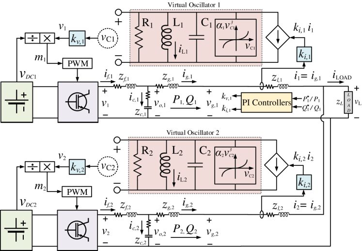
The system considered consists of two virtual oscillator controlled inverters with current feedback after the output LCL filter. A complete system overview is shown in Fig. 1. The filter parameters are zf=Rf+jωLfsubscript𝑧𝑓subscript𝑅𝑓𝑗superscript𝜔subscript𝐿𝑓z_{f}=R_{f}+j\omega^{*}L_{f}, zc=Rc+1jωCfsubscript𝑧𝑐subscript𝑅𝑐1𝑗superscript𝜔subscript𝐶𝑓z_{c}=R_{c}+\frac{1}{j\omega^{*}C_{f}} and zg=Rg+jωLgsubscript𝑧𝑔subscript𝑅𝑔𝑗superscript𝜔subscript𝐿𝑔z_{g}=R_{g}+j\omega^{*}L_{g}. The line impedance is represented as zl=Rl+jωLlsubscript𝑧𝑙subscript𝑅𝑙𝑗superscript𝜔subscript𝐿𝑙z_{l}=R_{l}+j\omega^{*}L_{l}. The inverters are connected to a common RL load zL=RL+jωLLsubscript𝑧𝐿subscript𝑅𝐿𝑗superscript𝜔subscript𝐿𝐿z_{L}=R_{L}+j\omega^{*}L_{L} through the point of common coupling (PCC). Moreover, inverter 111 can dispatch power by the use of two additional PI controllers.

Refer to caption
Figure 1: A overview of the overall system consisting of two parallel-connected virtual oscillator controlled inverters. The inverter 111 can dispatch power using the PI controllers while inverter 222 supplies the remaining power.

III System Modelling

In this section, the VOC dynamics are presented. Further, an averaged VOC model is derived for inverters with current feedback after the output LCL filter. The dynamics of the PI controllers used for power dispatch are the same as in [9].

III-A Virtual Oscillator Controller

A virtual oscillator consists of an LC harmonic oscillator with a fundamental frequency ω=1/LCsuperscript𝜔1𝐿𝐶\omega^{*}=1/\sqrt{LC}. It consists of a negative resistance element R=1/σ𝑅1𝜎R=-1/\sigma and a nonlinear current source with a positive constant α𝛼\alpha as shown in Fig. 1. The feedback current i𝑖i is scaled by the current feedback gain kisubscript𝑘𝑖k_{i} before entering the virtual oscillator. The vCsubscript𝑣𝐶v_{C} denotes the capacitor voltage and iLsubscript𝑖𝐿i_{L} denotes the inductor current. The capacitor voltage vCsubscript𝑣𝐶v_{C} is scaled by the voltage scaling factor kvsubscript𝑘𝑣k_{v} to generate the inverter output voltage v𝑣v. The actual VOC dynamics are given by the following dynamic equations [5]:

dVdt𝑑𝑉𝑑𝑡\displaystyle\frac{dV}{dt} =ϵω2(σg(2Vcos(ϕ))kvkii)cos(ϕ),absentitalic-ϵsuperscript𝜔2𝜎𝑔2𝑉italic-ϕsubscript𝑘𝑣subscript𝑘𝑖𝑖italic-ϕ\displaystyle=\frac{\epsilon\omega^{*}}{\sqrt{2}}\left(\sigma g\big{(}\sqrt{2}V\cos{(\phi)}\big{)}-k_{v}k_{i}i\right)\cos(\phi),
dϕdt𝑑italic-ϕ𝑑𝑡\displaystyle\frac{d\phi}{dt} =ωϵω2V(σg(2Vcos(ϕ))kvkii)sin(ϕ).absentsuperscript𝜔italic-ϵsuperscript𝜔2𝑉𝜎𝑔2𝑉italic-ϕsubscript𝑘𝑣subscript𝑘𝑖𝑖italic-ϕ\displaystyle=\omega^{*}-\frac{\epsilon\omega^{*}}{\sqrt{2}V}\left(\sigma g\big{(}\sqrt{2}V\cos(\phi)\big{)}-k_{v}k_{i}i\right)\sin(\phi). (1)

A detailed derivation and parametric description of the dynamical model for the inverter RMS output voltage magnitude V𝑉V and instantaneous phase angle ϕ=ωt+θitalic-ϕ𝜔𝑡𝜃\phi=\omega t+\theta where θ𝜃\theta is the phase offset with respect to ωt𝜔𝑡\omega t, can be found in [5].

III-B Averaged VOC Model for Inverters with Output LCL Filter

A new version of averaged VOC dynamics is presented for inverters with current feedback after the output LCL filter. A brief derivation is in Appendix -A. The proposed averaged VOC model is given by the following dynamic equations:

ddtV¯=σ2C(V¯β2V¯3)kvki2C(CαP¯V¯+SαQ¯V¯+CβV¯),𝑑𝑑𝑡¯𝑉𝜎2𝐶¯𝑉𝛽2superscript¯𝑉3subscript𝑘𝑣subscript𝑘𝑖2𝐶subscript𝐶𝛼¯𝑃¯𝑉subscript𝑆𝛼¯𝑄¯𝑉subscript𝐶𝛽¯𝑉\displaystyle\frac{d}{dt}\overline{V}=\frac{\sigma}{2C}\left(\overline{V}-\frac{\beta}{2}\overline{V}^{3}\right)-\frac{k_{v}k_{i}}{2C}\left(\frac{C_{\alpha}\overline{P}}{\overline{V}}+\frac{S_{\alpha}\overline{Q}}{\overline{V}}+C_{\beta}\overline{V}\right), (2)
ddtθ¯=ωω+kvki2C(CαQ¯V¯2SαP¯V¯2Sβ),𝑑𝑑𝑡¯𝜃superscript𝜔𝜔subscript𝑘𝑣subscript𝑘𝑖2𝐶subscript𝐶𝛼¯𝑄superscript¯𝑉2subscript𝑆𝛼¯𝑃superscript¯𝑉2subscript𝑆𝛽\displaystyle\frac{d}{dt}\overline{\theta}=\omega^{*}-\omega+\frac{k_{v}k_{i}}{2C}\left(\frac{C_{\alpha}\overline{Q}}{\overline{V}^{2}}-\frac{S_{\alpha}\overline{P}}{\overline{V}^{2}}-S_{\beta}\right), (3)

where β=3αkv2σ𝛽3𝛼superscriptsubscript𝑘𝑣2𝜎\beta=\frac{3\alpha}{k_{v}^{2}\sigma}, V¯¯𝑉\overline{V} denotes the averaged RMS output voltage magnitude and θ¯¯𝜃\overline{\theta} denotes the averaged phase offset with respect to ωt𝜔𝑡\omega t. The averaged active and reactive power are denoted by P¯¯𝑃\overline{P} and Q¯¯𝑄\overline{Q}, respectively. Cα,Cβ,Sαsubscript𝐶𝛼subscript𝐶𝛽subscript𝑆𝛼C_{\alpha},C_{\beta},S_{\alpha} and Sβsubscript𝑆𝛽S_{\beta} are the impedance constants (as defined in Appendix -A).

III-B1 Voltage Regulation Characteristics

The equilibrium value for the averaged RMS voltage magnitude V¯eqsubscript¯𝑉𝑒𝑞\overline{V}_{eq} can be determined by setting the left hand side of (2) to zero and solving for V¯¯𝑉\overline{V} as follows:

V¯eq=kvσβ±σβ26α(ki/kv)(CαP¯eq+SαQ¯eq)3α,subscript¯𝑉𝑒𝑞subscript𝑘𝑣plus-or-minussubscript𝜎𝛽superscriptsubscript𝜎𝛽26𝛼subscript𝑘𝑖subscript𝑘𝑣subscript𝐶𝛼subscript¯𝑃𝑒𝑞subscript𝑆𝛼subscript¯𝑄𝑒𝑞3𝛼\displaystyle\overline{V}_{eq}=k_{v}\sqrt{\frac{\sigma_{\beta}\pm\sqrt{\sigma_{\beta}^{2}-6\alpha\left(k_{i}/k_{v}\right)\left(C_{\alpha}\overline{P}_{eq}+S_{\alpha}\overline{Q}_{eq}\right)}}{3\alpha}}, (4)

where σβ=(σkvkiCβ)subscript𝜎𝛽𝜎subscript𝑘𝑣subscript𝑘𝑖subscript𝐶𝛽\sigma_{\beta}=\left(\sigma-k_{v}k_{i}C_{\beta}\right). The P¯eqsubscript¯𝑃𝑒𝑞\overline{P}_{eq} and Q¯eqsubscript¯𝑄𝑒𝑞\overline{Q}_{eq} denote the active and reactive power at the equilibrium. Both the roots of (4) are real valued if the following inequality holds:

(CαP¯+SαQ¯)<Scr:=σβ26α(ki/kv),subscript𝐶𝛼¯𝑃subscript𝑆𝛼¯𝑄subscript𝑆𝑐𝑟assignsuperscriptsubscript𝜎𝛽26𝛼subscript𝑘𝑖subscript𝑘𝑣\displaystyle\left(C_{\alpha}\overline{P}+S_{\alpha}\overline{Q}\right)<S_{cr}:=\frac{\sigma_{\beta}^{2}}{6\alpha\left(k_{i}/k_{v}\right)}, (5)

where ki>0subscript𝑘𝑖0k_{i}>0 and kv>0subscript𝑘𝑣0k_{v}>0. Scrsubscript𝑆𝑐𝑟S_{cr} denotes the critical power constant with corresponding critical value of the inverter RMS output voltage V¯cr=kvσβ3αsubscript¯𝑉𝑐𝑟subscript𝑘𝑣subscript𝜎𝛽3𝛼\overline{V}_{cr}=k_{v}\sqrt{\frac{\sigma_{\beta}}{3\alpha}}. A local stability analysis of the high voltage solution of (4) (similar to [5]) is not considered. In the subsequent analysis, we assume that the high voltage solution of (4) is locally asymptotically stable and with a slight abuse of notation, we denote it by V¯eqsubscript¯𝑉𝑒𝑞\overline{V}_{eq}. Using (4), the open circuit voltage V¯oc=kv2σβ3αsubscript¯𝑉𝑜𝑐subscript𝑘𝑣2subscript𝜎𝛽3𝛼\overline{V}_{oc}=k_{v}\sqrt{\frac{2\sigma_{\beta}}{3\alpha}} for the VO-controlled inverter (i.e. P¯eq=Q¯eq=0subscript¯𝑃𝑒𝑞subscript¯𝑄𝑒𝑞0\overline{P}_{eq}=\overline{Q}_{eq}=0).

III-B2 Frequency Regulation Characteristics

Solving the phase angle dynamics (3) for equilibrium point gives the system’s frequency ωeqsubscript𝜔𝑒𝑞\omega_{eq} in steady-state as follows:

ωeq=ω+kvki2C(CαQ¯eqV¯eq2SαP¯eqV¯eq2Sβ),subscript𝜔𝑒𝑞superscript𝜔subscript𝑘𝑣subscript𝑘𝑖2𝐶subscript𝐶𝛼subscript¯𝑄𝑒𝑞subscriptsuperscript¯𝑉2𝑒𝑞subscript𝑆𝛼subscript¯𝑃𝑒𝑞subscriptsuperscript¯𝑉2𝑒𝑞subscript𝑆𝛽\displaystyle\omega_{eq}=\omega^{*}+\frac{k_{v}k_{i}}{2C}\left(\frac{C_{\alpha}\overline{Q}_{eq}}{\overline{V}^{2}_{eq}}-\frac{S_{\alpha}\overline{P}_{eq}}{\overline{V}^{2}_{eq}}-S_{\beta}\right), (6)

where V¯eqsubscript¯𝑉𝑒𝑞\overline{V}_{eq} is the high voltage solution of (4).

III-B3 Dynamic Response

In order to quantify the dynamic response of the VO-controlled inverter, the time taken by the inverter to reach its open circuit voltage V¯ocsubscript¯𝑉𝑜𝑐\overline{V}_{oc} is considered. The following voltage dynamics of interest in a variable-separable ODE form are obtained from (2) by replacing P¯=Q¯=0¯𝑃¯𝑄0\overline{P}=\overline{Q}=0:

ddtV¯=σ2C(V¯β2V¯3)𝑑𝑑𝑡¯𝑉𝜎2𝐶¯𝑉𝛽2superscript¯𝑉3\displaystyle\frac{d}{dt}\overline{V}=\frac{\sigma}{2C}\left(\overline{V}-\frac{\beta}{2}\overline{V}^{3}\right) kvkiCβ2CV¯.subscript𝑘𝑣subscript𝑘𝑖subscript𝐶𝛽2𝐶¯𝑉\displaystyle-\frac{k_{v}k_{i}C_{\beta}}{2C}\overline{V}. (7)

The rise time trisesubscript𝑡𝑟𝑖𝑠𝑒t_{rise} is the time taken by the inverter to build-up output voltage from 0.1V¯oc0.1subscript¯𝑉𝑜𝑐0.1\overline{V}_{oc} to 0.9V¯oc0.9subscript¯𝑉𝑜𝑐0.9\overline{V}_{oc}. The trise6ωϵσβsubscript𝑡𝑟𝑖𝑠𝑒6superscript𝜔italic-ϵsubscript𝜎𝛽t_{rise}\approx\frac{6}{\omega^{*}\epsilon\sigma_{\beta}} is determined by separating variables in (7) and integrating under the limits from 0.1V¯oc0.1subscript¯𝑉𝑜𝑐0.1\overline{V}_{oc} to 0.9V¯oc0.9subscript¯𝑉𝑜𝑐0.9\overline{V}_{oc}, where ϵ=L/Citalic-ϵ𝐿𝐶\epsilon=\sqrt{L/C}.

III-C PI Controller Dynamics

The PI controller dynamics used to regulate active power are kv=KPp(P¯P)+epsubscript𝑘𝑣superscriptsubscript𝐾𝑃𝑝¯𝑃superscript𝑃subscript𝑒𝑝k_{v}=K_{P}^{p}(\overline{P}-P^{*})+e_{p} where e˙p=KIp(P¯P)subscript˙𝑒𝑝superscriptsubscript𝐾𝐼𝑝¯𝑃superscript𝑃\dot{e}_{p}=K_{I}^{p}(\overline{P}-P^{*}). Similarly, the PI controller dynamics used to regulate reactive power are ki=KPq(Q¯Q)+eqsubscript𝑘𝑖superscriptsubscript𝐾𝑃𝑞¯𝑄superscript𝑄subscript𝑒𝑞k_{i}=K_{P}^{q}(\overline{Q}-Q^{*})+e_{q} where e˙q=KIq(Q¯Q)subscript˙𝑒𝑞superscriptsubscript𝐾𝐼𝑞¯𝑄superscript𝑄\dot{e}_{q}=K_{I}^{q}(\overline{Q}-Q^{*}). The epsubscript𝑒𝑝e_{p} and eqsubscript𝑒𝑞e_{q} are the PI controllers’ states [9].

IV VOC Parameter Design Procedure

A parameter design procedure is presented for VO-controlled inverters with current feedback after the LCL filter. The parameters are selected such that the VO-controlled inverter satisfy the desired ac-performance specifications.

IV-A Designing the Scaling Factors

The voltage scaling factor kvsubscript𝑘𝑣k_{v} is chosen equal to V¯ocsubscript¯𝑉𝑜𝑐\overline{V}_{oc} to standardise the design procedure such that the virtual oscillator capacitor voltage is equal to 111 V RMS when the inverter’s output voltage is equal to V¯ocsubscript¯𝑉𝑜𝑐\overline{V}_{oc}. The current feedback gain kisubscript𝑘𝑖k_{i} is chosen as the ratio of V¯minsubscript¯𝑉𝑚𝑖𝑛\overline{V}_{min} to S¯maxsubscript¯𝑆𝑚𝑎𝑥\overline{S}_{max}. The V¯minsubscript¯𝑉𝑚𝑖𝑛\overline{V}_{min} corresponds to the constant S¯maxsubscript¯𝑆𝑚𝑎𝑥\overline{S}_{max} defined by:

S¯max=maxP¯2+Q¯2|S¯rated|2(CαP¯+SαQ¯).subscript¯𝑆𝑚𝑎𝑥subscriptsuperscript¯𝑃2superscript¯𝑄2superscriptsubscript¯𝑆𝑟𝑎𝑡𝑒𝑑2subscript𝐶𝛼¯𝑃subscript𝑆𝛼¯𝑄\displaystyle\overline{S}_{max}=\max_{\overline{P}^{2}+\overline{Q}^{2}\leq|\overline{S}_{rated}|^{2}}\left(C_{\alpha}\overline{P}+S_{\alpha}\overline{Q}\right). (8)

By choosing the gains as:

kv:=V¯oc,ki:=V¯minS¯max,formulae-sequenceassignsubscript𝑘𝑣subscript¯𝑉𝑜𝑐assignsubscript𝑘𝑖subscript¯𝑉𝑚𝑖𝑛subscript¯𝑆𝑚𝑎𝑥\displaystyle k_{v}:=\overline{V}_{oc},\quad\quad k_{i}:=\frac{\overline{V}_{min}}{\overline{S}_{max}}, (9)

the parallel-connected inverters in a system share the power proportional to their power ratings [5, 6].

IV-B Designing the Voltage Regulation Parameters

A design procedure for the virtual oscillator negative resistance element R=1σ𝑅1𝜎R=\frac{-1}{\sigma} and the coefficient of nonlinear current source α𝛼\alpha is presented. The proposed design procedure ensures the RMS output voltage to stay within the range: V¯minV¯eqV¯ocsubscript¯𝑉𝑚𝑖𝑛subscript¯𝑉𝑒𝑞subscript¯𝑉𝑜𝑐\overline{V}_{min}\leq\overline{V}_{eq}\leq\overline{V}_{oc} for S¯max(CαP¯eq+SαQ¯eq)0subscript¯𝑆𝑚𝑎𝑥subscript𝐶𝛼subscript¯𝑃𝑒𝑞subscript𝑆𝛼subscript¯𝑄𝑒𝑞0\overline{S}_{max}\geq\left(C_{\alpha}\overline{P}_{eq}+S_{\alpha}\overline{Q}_{eq}\right)\geq 0. The definition of Vocsubscript𝑉𝑜𝑐V_{oc} and the choice of kvsubscript𝑘𝑣k_{v} in (9) results in σ=3α2+kikvCβ𝜎3𝛼2subscript𝑘𝑖subscript𝑘𝑣subscript𝐶𝛽\sigma=\frac{3\alpha}{2}+k_{i}k_{v}C_{\beta}. Substituting (CαP¯eq+SαQ¯eq)=S¯maxsubscript𝐶𝛼subscript¯𝑃𝑒𝑞subscript𝑆𝛼subscript¯𝑄𝑒𝑞subscript¯𝑆𝑚𝑎𝑥\left(C_{\alpha}\overline{P}_{eq}+S_{\alpha}\overline{Q}_{eq}\right)=\overline{S}_{max}, V¯eq=V¯minsubscript¯𝑉𝑒𝑞subscript¯𝑉𝑚𝑖𝑛\overline{V}_{eq}=\overline{V}_{min}, kvsubscript𝑘𝑣k_{v} and kisubscript𝑘𝑖k_{i} as in (9), α=23σβ𝛼23subscript𝜎𝛽\alpha=\frac{2}{3}\sigma_{\beta} and σβ=(σkvkiCβ)subscript𝜎𝛽𝜎subscript𝑘𝑣subscript𝑘𝑖subscript𝐶𝛽\sigma_{\beta}=\left(\sigma-k_{v}k_{i}C_{\beta}\right) in the high voltage solution of (4), we get:

σ=V¯ocV¯minV¯oc2V¯oc2V¯min2+V¯minV¯ocCβS¯max.𝜎subscript¯𝑉𝑜𝑐subscript¯𝑉𝑚𝑖𝑛superscriptsubscript¯𝑉𝑜𝑐2superscriptsubscript¯𝑉𝑜𝑐2superscriptsubscript¯𝑉𝑚𝑖𝑛2subscript¯𝑉𝑚𝑖𝑛subscript¯𝑉𝑜𝑐subscript𝐶𝛽subscript¯𝑆𝑚𝑎𝑥\displaystyle\sigma=\frac{\overline{V}_{oc}}{\overline{V}_{min}}\frac{\overline{V}_{oc}^{2}}{\overline{V}_{oc}^{2}-\overline{V}_{min}^{2}}+\frac{\overline{V}_{min}\overline{V}_{oc}C_{\beta}}{\overline{S}_{max}}. (10)

IV-C Designing the Harmonic Oscillator Paramters

In order to derive a set of constraints to determine the parameters L𝐿L and C𝐶C, the frequency regulation characteristics (6), the rise time trisesubscript𝑡𝑟𝑖𝑠𝑒t_{rise} and the ratio of the amplitude of the third harmonic to the fundamental [5, Eq. 41] are considered. While designing the harmonic oscillator parameters, one of the design input is the maximum permissible frequency deviation |Δω|maxsubscriptΔ𝜔𝑚𝑎𝑥|\Delta\omega|_{max}. Let us start with the frequency regulation characteristics in (6) and define the following constant:

S¯|Δω|max=maxP¯2+Q¯2|S¯rated|2(CαQ¯SαP¯).subscript¯𝑆subscriptΔ𝜔𝑚𝑎𝑥subscriptsuperscript¯𝑃2superscript¯𝑄2superscriptsubscript¯𝑆𝑟𝑎𝑡𝑒𝑑2subscript𝐶𝛼¯𝑄subscript𝑆𝛼¯𝑃\displaystyle\overline{S}_{|\Delta\omega|_{max}}=\max_{\overline{P}^{2}+\overline{Q}^{2}\leq|\overline{S}_{rated}|^{2}}\left(C_{\alpha}\overline{Q}-S_{\alpha}\overline{P}\right). (11)

Using the worst-case operating condition for the output voltage (corresponding to S¯maxsubscript¯𝑆𝑚𝑎𝑥\overline{S}_{max} that results in the minimum permissible voltage V¯min)\overline{V}_{min}) and substituting the scaling factors from (9) into (6), the lower bound on capacitance C𝐶C is given by:

C12|Δω|max(S¯|Δω|maxV¯ocV¯minS¯maxSβV¯ocV¯minS¯max)=:C|Δω|maxmin.\displaystyle C\geq\frac{1}{2|\Delta\omega|_{max}}\left(\frac{\overline{S}_{|\Delta\omega|_{max}}\overline{V}_{oc}}{\overline{V}_{min}\overline{S}_{max}}-\frac{S_{\beta}\overline{V}_{oc}\overline{V}_{min}}{\overline{S}_{max}}\right)=:C_{|\Delta\omega|_{max}}^{min}. (12)

Define the maximum permissible rise time trisemaxsuperscriptsubscript𝑡𝑟𝑖𝑠𝑒𝑚𝑎𝑥t_{rise}^{max} as the design input. Now, considering the trisesubscript𝑡𝑟𝑖𝑠𝑒t_{rise} of an unloaded inverter and (10), the upper bound on the capacitance C𝐶C is defined as:

Ctrisemax6V¯ocV¯minV¯oc2V¯oc2V¯min2=:Ctrisemax.\displaystyle C\leq\frac{t_{rise}^{max}}{6}\frac{\overline{V}_{oc}}{\overline{V}_{min}}\frac{\overline{V}_{oc}^{2}}{\overline{V}_{oc}^{2}-\overline{V}_{min}^{2}}=:C_{t_{rise}^{max}}. (13)

Finally, the third design input is the maximum-permissible ratio of the amplitude of third harmonic to the fundamental δ3:1maxsuperscriptsubscript𝛿:31𝑚𝑎𝑥\delta_{3:1}^{max} where δ3:1=ϵσ8subscript𝛿:31italic-ϵ𝜎8\delta_{3:1}=\frac{\epsilon\sigma}{8} as defined in [5, Eq. 41]. Replacing (10) in the expression for δ3:1maxsuperscriptsubscript𝛿:31𝑚𝑎𝑥\delta_{3:1}^{max}, we get another lower bound on the capacitance C𝐶C given by:

C(18ωδ3:1max)(V¯ocV¯minV¯oc2V¯oc2V¯min2+V¯minV¯ocCβS¯max)=:Cδ3:1min.\displaystyle C\geq\left(\frac{1}{8\omega^{*}\delta_{3:1}^{max}}\right)\left(\frac{\overline{V}_{oc}}{\overline{V}_{min}}\frac{\overline{V}_{oc}^{2}}{\overline{V}_{oc}^{2}-\overline{V}_{min}^{2}}+\frac{\overline{V}_{min}\overline{V}_{oc}C_{\beta}}{\overline{S}_{max}}\right)=:C_{\delta_{3:1}}^{min}. (14)

The constraints (12)-(14) define a permissible range for the capacitance satisfying the desired frequency regulation, rise time and harmonic distortion specifications. The permissible range of capacitance C𝐶C can be written as:

max{C|Δω|maxmin,Cδ3:1min}CCtrisemax.𝑚𝑎𝑥superscriptsubscript𝐶subscriptΔ𝜔𝑚𝑎𝑥𝑚𝑖𝑛superscriptsubscript𝐶subscript𝛿:31𝑚𝑖𝑛𝐶subscript𝐶superscriptsubscript𝑡𝑟𝑖𝑠𝑒𝑚𝑎𝑥\displaystyle max\{C_{|\Delta\omega|_{max}}^{min},C_{\delta_{3:1}}^{min}\}\leq C\leq C_{t_{rise}^{max}}. (15)

Once the value is chosen for the capacitance C𝐶C, the inductance can be determined as L=1C(ω)2𝐿1𝐶superscriptsuperscript𝜔2L=\frac{1}{C(\omega^{*})^{2}}. Note that it may be possible (15) does not hold for the set of design inputs {|Δω|max,trisemax,δ3:1max}subscriptΔ𝜔𝑚𝑎𝑥superscriptsubscript𝑡𝑟𝑖𝑠𝑒𝑚𝑎𝑥superscriptsubscript𝛿:31𝑚𝑎𝑥\{|\Delta\omega|_{max},t_{rise}^{max},\delta_{3:1}^{max}\} and necessitates a design trade-off.

V Power Dispatch

The power dispatch technique presented in [9] is extended to the averaged VOC model with current feedback after the output LCL filter. Inverter 111 simultaneously regulates both the active and reactive power according to the desired power set-point (P1,Q1)superscriptsubscript𝑃1superscriptsubscript𝑄1(P_{1}^{*},Q_{1}^{*}) using the PI controllers that continuously tune the VOC parameters kv,1subscript𝑘𝑣1k_{v,1} and ki,1subscript𝑘𝑖1k_{i,1} as in [9].

V-A Power Security Constraint

An updated power security constraint is derived to determine the achievable power set-points and guarantee the existence of real valued control inputs.

Theorem 1.

Assuming the averaged model of two VOC inverters with current feedback after the output LCL filter that synchronise to a common frequency, and are connected to a common fixed impedance load zLsubscript𝑧𝐿z_{L} through line impedance values zl,1subscript𝑧𝑙1z_{l,1} and zl,2subscript𝑧𝑙2z_{l,2}, respectively, the desired output power set-point P¯1superscriptsubscript¯𝑃1\overline{P}_{1}^{*} and Q¯1superscriptsubscript¯𝑄1\overline{Q}_{1}^{*} for inverter 111 can be achieved and there exists corresponding real-valued current feedback gain ki,1ιsuperscriptsubscript𝑘𝑖1𝜄k_{i,1}^{\iota} and voltage scaling factor kv,1ιsuperscriptsubscript𝑘𝑣1𝜄k_{v,1}^{\iota}, if the following security constraint is satisfied for the averaged VOC-dynamics:

σ1V¯1ι2μ(Cα,1P¯1+Sα,1Q¯1+Cβ,1V¯1ι2)>0,subscript𝜎1superscriptsuperscriptsubscript¯𝑉1𝜄2𝜇subscript𝐶𝛼1superscriptsubscript¯𝑃1subscript𝑆𝛼1superscriptsubscript¯𝑄1subscript𝐶𝛽1superscriptsuperscriptsubscript¯𝑉1𝜄20\displaystyle\sigma_{1}{\overline{V}_{1}^{\iota}}^{2}-\mu\left(C_{\alpha,1}\overline{P}_{1}^{*}+S_{\alpha,1}\overline{Q}_{1}^{*}+C_{\beta,1}{\overline{V}_{1}^{\iota}}^{2}\right)>0, (16)

where,

μ=kv,1ιki,1ι=kv,2ki,2(Cα,2Q¯2ιSα,2P¯2ιV¯2ι2Sβ,2)(Cα,1Q¯1Sα,1P¯1V¯1ι2Sβ,1).𝜇superscriptsubscript𝑘𝑣1𝜄superscriptsubscript𝑘𝑖1𝜄subscript𝑘𝑣2subscript𝑘𝑖2subscript𝐶𝛼2superscriptsubscript¯𝑄2𝜄subscript𝑆𝛼2superscriptsubscript¯𝑃2𝜄superscriptsuperscriptsubscript¯𝑉2𝜄2subscript𝑆𝛽2subscript𝐶𝛼1superscriptsubscript¯𝑄1subscript𝑆𝛼1superscriptsubscript¯𝑃1superscriptsuperscriptsubscript¯𝑉1𝜄2subscript𝑆𝛽1\displaystyle\mu=k_{v,1}^{\iota}k_{i,1}^{\iota}=k_{v,2}k_{i,2}\frac{\left(\frac{C_{\alpha,2}\overline{Q}_{2}^{\iota}-S_{\alpha,2}\overline{P}_{2}^{\iota}}{{\overline{V}_{2}^{\iota}}^{2}}-S_{\beta,2}\right)}{\left(\frac{C_{\alpha,1}\overline{Q}_{1}^{*}-S_{\alpha,1}\overline{P}_{1}^{*}}{{\overline{V}_{1}^{\iota}}^{2}}-S_{\beta,1}\right)}. (17)

V¯2ιsuperscriptsubscript¯𝑉2𝜄\overline{V}_{2}^{\iota} and Q¯2ιsuperscriptsubscript¯𝑄2𝜄\overline{Q}_{2}^{\iota} denote the steady-state averaged output voltage magnitude and reactive power supplied by inverter 222, respectively, corresponding to the desired power set-point (P¯1,Q¯1superscriptsubscript¯𝑃1superscriptsubscript¯𝑄1\overline{P}_{1}^{*},\overline{Q}_{1}^{*}).

The proof of this theorem is similar to [9, Theorem 1] and is omitted due to the space limitation. The updated control laws to determine the control inputs kv,1ιsuperscriptsubscript𝑘𝑣1𝜄k_{v,1}^{\iota} and ki,1ιsuperscriptsubscript𝑘𝑖1𝜄k_{i,1}^{\iota} corresponding to the desired power set-point (P¯1,Q¯1)superscriptsubscript¯𝑃1superscriptsubscript¯𝑄1(\overline{P}_{1}^{*},\overline{Q}_{1}^{*}) are:

kv,1ι=±(σ1μCβ,1)V¯1ι4(σ1μCβ,1)V¯1ι2μ(Cα,1P¯1+Sα,1Q¯1),ki,1ι=μkv,1ι.formulae-sequencesuperscriptsubscript𝑘𝑣1𝜄plus-or-minussubscript𝜎1𝜇subscript𝐶𝛽1superscriptsuperscriptsubscript¯𝑉1𝜄4subscript𝜎1𝜇subscript𝐶𝛽1superscriptsuperscriptsubscript¯𝑉1𝜄2𝜇subscript𝐶𝛼1superscriptsubscript¯𝑃1subscript𝑆𝛼1superscriptsubscript¯𝑄1superscriptsubscript𝑘𝑖1𝜄𝜇superscriptsubscript𝑘𝑣1𝜄\displaystyle k_{v,1}^{\iota}=\pm\sqrt{\frac{\left(\sigma_{1}-\mu C_{\beta,1}\right){\overline{V}_{1}^{\iota}}^{4}}{\left(\sigma_{1}-\mu C_{\beta,1}\right){\overline{V}_{1}^{\iota}}^{2}-\mu\left(C_{\alpha,1}\overline{P}_{1}^{*}+S_{\alpha,1}\overline{Q}_{1}^{*}\right)}},\,k_{i,1}^{\iota}=\frac{\mu}{k_{v,1}^{\iota}}. (18)

VI Simulation Results

Simulation results in MATLAB (with ideal voltage sources) are presented for a number of scenarios to validate the proposed averaged model. The line, load and filter parameters Rf=Rl=0.15Ωsubscript𝑅𝑓subscript𝑅𝑙0.15ΩR_{f}=R_{l}=0.15\,\Omega, Lf=Ll=2.48subscript𝐿𝑓subscript𝐿𝑙2.48L_{f}=L_{l}=2.48 mH, Rc=3.3Ωsubscript𝑅𝑐3.3ΩR_{c}=3.3\,\Omega, Cf=4.7μsubscript𝐶𝑓4.7𝜇C_{f}=4.7\,\muF, Rg=0.13Ωsubscript𝑅𝑔0.13ΩR_{g}=0.13\,\Omega, Lg=0.97subscript𝐿𝑔0.97L_{g}=0.97 mH, RL=22.1Ωsubscript𝑅𝐿22.1ΩR_{L}=22.1\,\Omega and LL=14.4subscript𝐿𝐿14.4L_{L}=14.4 mH. The system parameters and ac-performance specifications are as in Table I and Table II.

Table I: System Parameters
Symbol Parameter Inverter 111 Inverter 222 Unit
kisubscript𝑘𝑖k_{i} Current feedback gain 0.152250.152250.15225 0.152250.152250.15225 A/A
kvsubscript𝑘𝑣k_{v} Voltage scaling factor 126 126126126 V/V
σ𝜎\sigma Conductance 6.092566.092566.09256 6.092566.092566.09256 Ω1superscriptΩ1\Omega^{-1}
α𝛼\alpha Cubic-current source coefficient 4.061844.061844.06184 4.061844.061844.06184 A/V3
L𝐿L Oscillator inductance 34.66134.66134.661 34.66134.66134.661 μ𝜇\muH
C𝐶C Oscillator capacitance 0.2030.2030.203 0.2030.2030.203 F
Table II: AC Performance Specifications
Symbol Parameter Value Unit
V¯ocsubscript¯𝑉𝑜𝑐\overline{V}_{oc} RMS open-circuit voltage 126126126 V
V¯minsubscript¯𝑉𝑚𝑖𝑛\overline{V}_{min} RMS rated power voltage 114114114 V
P¯ratedsubscript¯𝑃𝑟𝑎𝑡𝑒𝑑\overline{P}_{rated} Rated real power 750750750 W
|Q¯rated|subscript¯𝑄𝑟𝑎𝑡𝑒𝑑|\overline{Q}_{rated}| Rated reactive power 750750750 VAr
ωsuperscript𝜔\omega^{*} Nominal oscillator frequency 2π602𝜋602\pi 60 rad/s
|Δω|maxsubscriptΔ𝜔𝑚𝑎𝑥|\Delta\omega|_{max} Maximum frequency offset 2π0.52𝜋0.52\pi 0.5 rad/s
trisemaxsuperscriptsubscript𝑡𝑟𝑖𝑠𝑒𝑚𝑎𝑥t_{rise}^{max} Maximum rise time 0.20.20.2 s
δ3:1maxsuperscriptsubscript𝛿:31𝑚𝑎𝑥\delta_{3:1}^{max} 3rdsuperscript3rd3^{\mbox{rd}} to 1stsuperscript1st1^{\mbox{st}} harmonic ratio 111 %percent\%

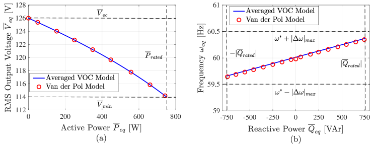
VI-A Embedded Droop Characteristics

In order to validate the embedded droop characteristics (4), (6) within the averaged VOC dynamics, a comparison is made with the actual VOC dynamics (III-A) with current feedback after the LCL filter. In Fig. 2, it can be seen that the embedded droop characteristics are close to the actual VOC dynamics. In order to obtain the V¯P¯¯𝑉¯𝑃\overline{V}-\overline{P} and ωQ¯𝜔¯𝑄\omega-\overline{Q} droop characteristics, the LCL filter is assumed to be ideal (i.e. Rf=Rc=Rg=0subscript𝑅𝑓subscript𝑅𝑐subscript𝑅𝑔0R_{f}=R_{c}=R_{g}=0) resulting in Sα=0subscript𝑆𝛼0S_{\alpha}=0 and the parameters in Table I are re-derived according to the design procedure in Section IV.

Refer to caption
Figure 2: A comparison between the embedded droop characteristics within the averaged VOC dynamics (2)-(3) and actual VOC dynamics (III-A).

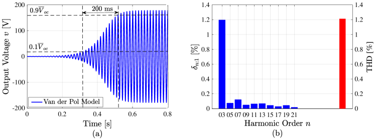
VI-B Rise Time and Harmonics Analysis

In Fig. 3, the rise time and harmonics analysis is presented for an unloaded inverter. It can be seen that the VO-controlled inverter closely follows the design inputs trisemaxsuperscriptsubscript𝑡𝑟𝑖𝑠𝑒𝑚𝑎𝑥t_{rise}^{max} and δ3:1maxsuperscriptsubscript𝛿:31𝑚𝑎𝑥\delta_{3:1}^{max}, thus validating the parameter design procedure in Section IV.

Refer to caption
Figure 3: The rise time and harmonics analysis shows that the virtual oscillator controlled inverter closely follows the desired design inputs trisemaxsuperscriptsubscript𝑡𝑟𝑖𝑠𝑒𝑚𝑎𝑥t_{rise}^{max} and δ3:1maxsuperscriptsubscript𝛿:31𝑚𝑎𝑥\delta_{3:1}^{max}.

VI-C Models Comparison

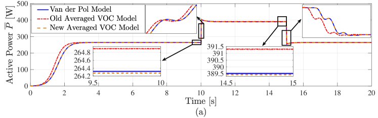
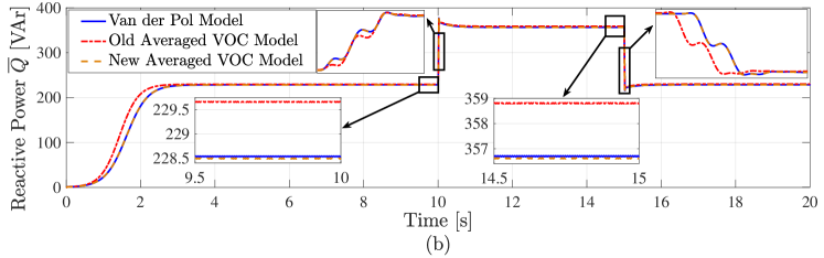
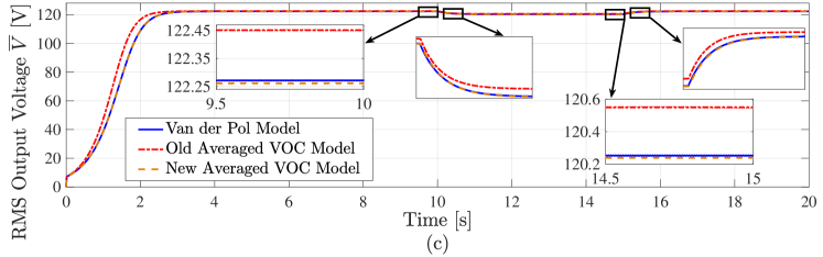
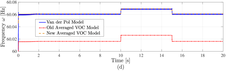
In Fig. 4, a comparison is made between the previously reported averaged VOC model [5], the proposed averaged VOC model (2)-(3) and actual VOC dynamics (III-A). Note that the proposed averaged VOC model follows the actual VOC dynamics more closely as compared to the previously reported averaged VOC model. For comparison, the LCL filter is chosen with higher values of filter parameters (Lfι=10Lf,Cfι=19.75Cfformulae-sequencesuperscriptsubscript𝐿𝑓𝜄10subscript𝐿𝑓superscriptsubscript𝐶𝑓𝜄19.75subscript𝐶𝑓L_{f}^{\iota}=10L_{f},C_{f}^{\iota}=19.75C_{f}) and the epsilon is chosen to be ϵι=ϵ8=L/C8superscriptitalic-ϵ𝜄italic-ϵ8𝐿𝐶8\epsilon^{\iota}=\frac{\epsilon}{8}=\frac{\sqrt{L/C}}{8}. The zL=6.9+j16.6Ωsubscript𝑧𝐿6.9𝑗16.6Ωz_{L}=6.9+j16.6\,\Omega with zS=44.24+j10.85Ωsubscript𝑧𝑆44.24𝑗10.85Ωz_{S}=44.24+j10.85\,\Omega in-parallel to implement the step-up and step-down changes. The system parameters in Table I are re-derived according to the design procedure in Section IV. Note that the difference between the previously reported averaged VOC model and actual VOC dynamics starts to increase for a higher value of filter capacitance. The output power is computed using a moving average window where window’s length is updated based on the frequency recovered from actual VOC dynamics.
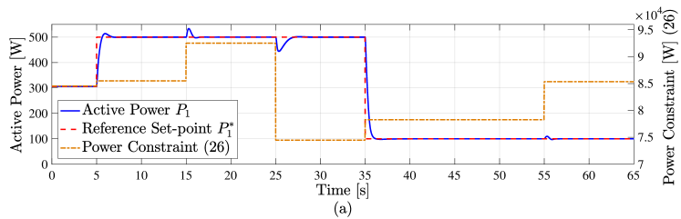
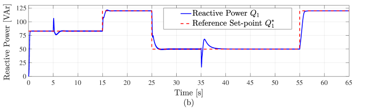
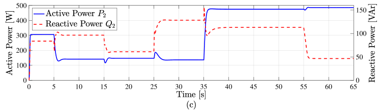
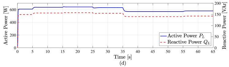
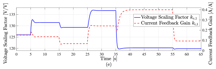
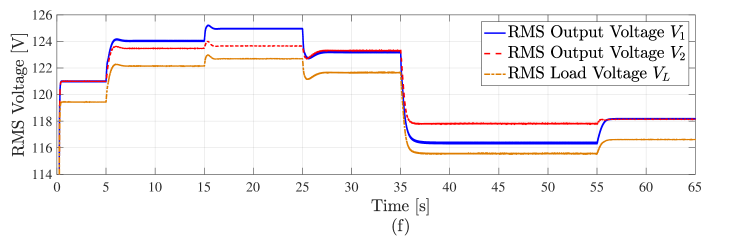
Refer to caption
Refer to caption
Refer to caption
Refer to caption
Figure 4: Comparison between previously reported averaged VOC model [5], the proposed averaged VOC model (2)-(3) and actual VOC dynamics (III-A): (a) active power, (b) reactive power, (c) voltages, (d) frequency.

VI-D Power Dispatch

In Fig. 5, the power dispatch results are presented for a number of scenarios as listed in Table III. Inverter 111 simultaneously regulates both the active and reactive power using the two PI controllers [9] that continuously tune the voltage scaling factor kv,1subscript𝑘𝑣1k_{v,1} and current feedback gain ki,1subscript𝑘𝑖1k_{i,1}. The inverter 222 supplies the remaining power to the load acting like a slack bus. The PI controllers’ proportional and integral gains are KPp=0.001superscriptsubscript𝐾𝑃𝑝0.001K_{P}^{p}=-0.001, KIp=0.15superscriptsubscript𝐾𝐼𝑝0.15K_{I}^{p}=-0.15, KPq=0.0001superscriptsubscript𝐾𝑃𝑞0.0001K_{P}^{q}=0.0001 and KIq=0.01superscriptsubscript𝐾𝐼𝑞0.01K_{I}^{q}=0.01. In Fig. 5, inverter 111 tracks the desired power set-points effectively while satisfying the security constraint (16). The corresponding changes in the inverter 222 power, load power, control inputs and voltages are also presented.

Refer to caption
Refer to caption
Refer to caption
Refer to caption
Refer to caption
Refer to caption
Figure 5: Power dispatch results for inverter 111 while inverter 222 supplies the remaining load power: (a) inverter 111 active power, power security constraint and reference set-point, (b) inverter 111 reactive power and reference set-point, (c) inverter 222 output power, (d) load power, (e) control inputs, (f) voltages.
Table III: Power Dispatch Set-points
Case No. P1superscriptsubscript𝑃1P_{1}^{*} [W] Q1superscriptsubscript𝑄1Q_{1}^{*} [VAr] Time [s]
111 - - 05050-5
222 500500500 838383 5155155-15
333 500500500 120120120 1525152515-25
444 500500500 505050 2535253525-35
555 100100100 505050 3555355535-55
666 100100100 120120120 5565556555-65

VII Conclusion

The LCL filter is considered an essential part of commercial inverters to filter out the harmonics and improve the output voltage. Keeping this in view, an averaged VOC model is derived for inverters with current feedback after the output LCL filter. The averaged model uncovers the embedded droop-characteristics within the averaged VOC dynamics and simplifies the analysis. The voltage and frequency regulation characteristics are determined. Further, to enable the VO-controlled inverter to satisfy the desired ac-performance specifications, a parameter design procedure is presented. Moreover, a recently reported power dispatch technique is extended to the proposed averaged VOC model with current feedback after the output LCL filter. The updated control laws are derived to determine the control inputs corresponding to a particular power set-point. An updated power security constraint is derived to determine the feasible operating region. The power security constraint is helpful in planning the optimal power flow in an electric grid. The simulation results validate the proposed averaged VOC model and power dispatch technique. Future work can include generalising the method to multiple inverters, stability analysis and experimental validation.

-A Derivation of the Averaged VOC Model with an LCL Filter

Consider an inverter with current feedback after the output LCL filter as shown in Fig. 1. Let us denote a phasor associated with a time domain variable (.)(.) by (.)\overrightarrow{(.)}. The V𝑉\overrightarrow{V} denotes the voltage before the LCL filter, the Vosubscript𝑉𝑜\overrightarrow{V_{o}} denotes the filter capacitor voltage and the Vgsubscript𝑉𝑔\overrightarrow{V_{g}} denotes the voltage after the LCL filter. Similarly, the Ifsubscript𝐼𝑓\overrightarrow{I_{f}} denotes the current flowing through filter inductor Lfsubscript𝐿𝑓L_{f}, the Icsubscript𝐼𝑐\overrightarrow{I_{c}} denotes the filter capacitor current and the Igsubscript𝐼𝑔\overrightarrow{I_{g}} is the current flowing through filter inductor Lgsubscript𝐿𝑔L_{g}. Solving the network equations, we have:

Ig=[ZαθαZβθβ][IfV],subscript𝐼𝑔delimited-[]subscript𝑍𝛼subscript𝜃𝛼subscript𝑍𝛽subscript𝜃𝛽delimited-[]subscript𝐼𝑓𝑉\displaystyle\overrightarrow{I_{g}}=\left[\begin{array}[]{cc}Z_{\alpha}\angle\theta_{\alpha}&Z_{\beta}\angle\theta_{\beta}\end{array}\right]\left[\begin{array}[]{c}\overrightarrow{I_{f}}\\ \overrightarrow{V}\end{array}\right], (22)

where zα=Zαθα=zc+zfzcsubscript𝑧𝛼subscript𝑍𝛼subscript𝜃𝛼subscript𝑧𝑐subscript𝑧𝑓subscript𝑧𝑐z_{\alpha}=Z_{\alpha}\angle\theta_{\alpha}=\frac{z_{c}+z_{f}}{z_{c}} and zβ=Zβθβ=1zcsubscript𝑧𝛽subscript𝑍𝛽subscript𝜃𝛽1subscript𝑧𝑐z_{\beta}=Z_{\beta}\angle\theta_{\beta}=\frac{-1}{z_{c}} are the impedance constants defined at ωsuperscript𝜔\omega^{*}. Further, we have [5]:

ddtϕ=ω+ddtθ=ω+ddtθ,𝑑𝑑𝑡italic-ϕsuperscript𝜔𝑑𝑑𝑡superscript𝜃𝜔𝑑𝑑𝑡𝜃\displaystyle\frac{d}{dt}\phi=\omega^{*}+\frac{d}{dt}\theta^{*}=\omega+\frac{d}{dt}\theta, (23)

where the instantaneous phase angle is denoted by ϕitalic-ϕ\phi, the nominal grid frequency is denoted by ωsuperscript𝜔\omega^{*} and the load dependent steady-state frequency is denoted by ω𝜔\omega. The angles θsuperscript𝜃\theta^{*} and θ𝜃\theta denote the phase offset with respect to ωtsuperscript𝜔𝑡\omega^{*}t and ωt𝜔𝑡\omega t, respectively. The inverter output voltage is given by:

v(t)=2V(t)cos(ωt+θ(t)).𝑣𝑡2𝑉𝑡superscript𝜔𝑡superscript𝜃𝑡\displaystyle v(t)=\sqrt{2}V(t)\cos{(\omega^{*}t+\theta^{*}(t))}. (24)

The instantaneous active and reactive output power of inverter in terms of v(t)𝑣𝑡v(t) and i(t)𝑖𝑡i(t) is given by:

P(t)=v(t)i(t),Q(t)=v(tπ2)i(t).formulae-sequence𝑃𝑡𝑣𝑡𝑖𝑡𝑄𝑡𝑣𝑡𝜋2𝑖𝑡\displaystyle P(t)=v(t)i(t),\quad\quad Q(t)=v\left(t-\frac{\pi}{2}\right)i(t). (25)

The averaged active and reactive power over an ac-cycle 2πω2𝜋superscript𝜔\frac{2\pi}{\omega^{*}} is defined as:

P¯(t)=ω2πs=tt+2π/ωP(s)𝑑s,Q¯(t)=ω2πs=tt+2π/ωQ(s)𝑑s.formulae-sequence¯𝑃𝑡superscript𝜔2𝜋superscriptsubscript𝑠𝑡𝑡2𝜋superscript𝜔𝑃𝑠differential-d𝑠¯𝑄𝑡superscript𝜔2𝜋superscriptsubscript𝑠𝑡𝑡2𝜋superscript𝜔𝑄𝑠differential-d𝑠\displaystyle\overline{P}(t)=\frac{\omega^{*}}{2\pi}\int_{s=t}^{t+2\pi/\omega^{*}}P(s)ds,\quad\overline{Q}(t)=\frac{\omega^{*}}{2\pi}\int_{s=t}^{t+2\pi/\omega^{*}}Q(s)ds. (26)

In order to derive the averaged dynamics (2)-(3), a change of variable is made from tτ=ωt𝑡𝜏superscript𝜔𝑡t\rightarrow\tau=\omega^{*}t and θ(τ)=ϕ(τ/ω)τsuperscript𝜃𝜏italic-ϕ𝜏superscript𝜔𝜏\theta^{*}(\tau)=\phi(\tau/\omega^{*})-\tau. Expressing the actual VOC dynamics (III-A) as a function of θsuperscript𝜃\theta^{*}, we have [5]:

dVdτ𝑑𝑉𝑑𝜏\displaystyle\frac{dV}{d\tau} =ϵ2(σg(2Vcos(τ+θ))kvkii)cos(τ+θ),absentitalic-ϵ2𝜎𝑔2𝑉𝜏superscript𝜃subscript𝑘𝑣subscript𝑘𝑖𝑖𝜏superscript𝜃\displaystyle=\frac{\epsilon}{\sqrt{2}}\left(\sigma g\big{(}\sqrt{2}V\cos{(\tau+\theta^{*})}\big{)}-k_{v}k_{i}i\right)\cos{(\tau+\theta^{*})},
dθdτ𝑑superscript𝜃𝑑𝜏\displaystyle\frac{d\theta^{*}}{d\tau} =ϵ2V(σg(2Vcos(τ+θ))kvkii)sin(τ+θ).absentitalic-ϵ2𝑉𝜎𝑔2𝑉𝜏superscript𝜃subscript𝑘𝑣subscript𝑘𝑖𝑖𝜏superscript𝜃\displaystyle=-\frac{\epsilon}{\sqrt{2}V}\left(\sigma g\big{(}\sqrt{2}V\cos{(\tau+\theta^{*})}\big{)}-k_{v}k_{i}i\right)\sin{(\tau+\theta^{*})}. (27)

The dynamics in (-A) are 2π2𝜋2\pi periodic functions in τ𝜏\tau. The averaged dynamics in the quasi-harmonic limit ϵ0italic-ϵ0\epsilon\searrow 0 (following [5, Eq. 12]) are given by:

[V¯˙θ¯˙]=delimited-[]˙¯𝑉superscript˙¯𝜃absent\displaystyle\left[\begin{array}[]{c}\dot{\overline{V}}\\ \dot{\overline{\theta}}^{*}\end{array}\right]= ϵσ2π202πg(2V¯cos(τ+θ¯))[cos(τ+θ¯)1V¯sin(τ+θ¯)]𝑑τitalic-ϵ𝜎2𝜋2superscriptsubscript02𝜋𝑔2¯𝑉𝜏superscript¯𝜃delimited-[]𝜏superscript¯𝜃1¯𝑉𝜏superscript¯𝜃differential-d𝜏\displaystyle\frac{\epsilon\sigma}{2\pi\sqrt{2}}\int_{0}^{2\pi}g\left(\sqrt{2}\overline{V}\cos{(\tau+\overline{\theta}^{*})}\right)\left[\begin{array}[]{c}\cos{(\tau+\overline{\theta}^{*})}\\ \frac{-1}{\overline{V}}\sin{(\tau+\overline{\theta}^{*})}\end{array}\right]d\tau (32)
ϵkvki2π202πi[cos(τ+θ¯)1V¯sin(τ+θ¯)]𝑑τ,italic-ϵsubscript𝑘𝑣subscript𝑘𝑖2𝜋2superscriptsubscript02𝜋𝑖delimited-[]𝜏superscript¯𝜃1¯𝑉𝜏superscript¯𝜃differential-d𝜏\displaystyle-\frac{\epsilon k_{v}k_{i}}{2\pi\sqrt{2}}\int_{0}^{2\pi}i\left[\begin{array}[]{c}\cos{(\tau+\overline{\theta}^{*})}\\ \frac{-1}{\overline{V}}\sin{(\tau+\overline{\theta}^{*})}\end{array}\right]d\tau, (35)
=\displaystyle= ϵσ2[V¯β2V¯30]ϵkvki2π202πi[cos(τ+θ¯)1V¯sin(τ+θ¯)]𝑑τ.italic-ϵ𝜎2delimited-[]¯𝑉𝛽2superscript¯𝑉30italic-ϵsubscript𝑘𝑣subscript𝑘𝑖2𝜋2superscriptsubscript02𝜋𝑖delimited-[]𝜏superscript¯𝜃1¯𝑉𝜏superscript¯𝜃differential-d𝜏\displaystyle\frac{\epsilon\sigma}{2}\left[\begin{array}[]{c}\overline{V}-\frac{\beta}{2}\overline{V}^{3}\\ 0\end{array}\right]-\frac{\epsilon k_{v}k_{i}}{2\pi\sqrt{2}}\int_{0}^{2\pi}i\left[\begin{array}[]{c}\cos{(\tau+\overline{\theta}^{*})}\\ \frac{-1}{\overline{V}}\sin{(\tau+\overline{\theta}^{*})}\end{array}\right]d\tau. (40)

Changing the coordinates from τ𝜏\tau to t𝑡t in (32) and keeping the 𝒪(ϵ)𝒪italic-ϵ\mathcal{O}(\epsilon) terms only, we have:

ddt[V¯θ¯]𝑑𝑑𝑡delimited-[]¯𝑉superscript¯𝜃\displaystyle\frac{d}{dt}\left[\begin{array}[]{c}\overline{V}\\ \overline{\theta}^{*}\end{array}\right] =σ2C[V¯β2V¯30]absent𝜎2𝐶delimited-[]¯𝑉𝛽2superscript¯𝑉30\displaystyle=\frac{\sigma}{2C}\left[\begin{array}[]{c}\overline{V}-\frac{\beta}{2}\overline{V}^{3}\\ 0\end{array}\right] (45)
kvkiω2π2C02πωi(t)[cos(ωt+θ¯)1V¯sin(ωt+θ¯)]𝑑t.subscript𝑘𝑣subscript𝑘𝑖superscript𝜔2𝜋2𝐶superscriptsubscript02𝜋superscript𝜔𝑖𝑡delimited-[]superscript𝜔𝑡superscript¯𝜃1¯𝑉superscript𝜔𝑡superscript¯𝜃differential-d𝑡\displaystyle-\frac{k_{v}k_{i}\omega^{*}}{2\pi\sqrt{2}C}\int_{0}^{\frac{2\pi}{\omega^{*}}}i(t)\left[\begin{array}[]{c}\cos{(\omega^{*}t+\overline{\theta}^{*})}\\ \frac{-1}{\overline{V}}\sin{(\omega^{*}t+\overline{\theta}^{*})}\end{array}\right]dt. (48)

Lets define the impedance constants Cα=Zαcosθαsubscript𝐶𝛼subscript𝑍𝛼subscript𝜃𝛼C_{\alpha}=Z_{\alpha}\cos{\theta_{\alpha}}, Cβ=Zβcosθβsubscript𝐶𝛽subscript𝑍𝛽subscript𝜃𝛽C_{\beta}=Z_{\beta}\cos{\theta_{\beta}}, Sα=Zαsinθαsubscript𝑆𝛼subscript𝑍𝛼subscript𝜃𝛼S_{\alpha}=Z_{\alpha}\sin{\theta_{\alpha}} and Sβ=Zβsinθβsubscript𝑆𝛽subscript𝑍𝛽subscript𝜃𝛽S_{\beta}=Z_{\beta}\sin{\theta_{\beta}}. The current i=2Icos(ωt+θi)𝑖2𝐼superscript𝜔𝑡superscriptsubscript𝜃𝑖i=\sqrt{2}I\cos{(\omega^{*}t+\theta_{i}^{*})} where I𝐼I is the RMS current magnitude and θisuperscriptsubscript𝜃𝑖\theta_{i}^{*} is the phase-offset with respect to ωtsuperscript𝜔𝑡\omega^{*}t. Let Igsuperscriptsubscript𝐼𝑔\overrightarrow{I_{g}}^{\Re} denotes the real part of the current Igsubscript𝐼𝑔\overrightarrow{I_{g}} (22) and is given by:

Ig=2(ZαIcos(ωt+θi+θα)+ZβVcos(ωt+θ+θβ)).superscriptsubscript𝐼𝑔2subscript𝑍𝛼𝐼superscript𝜔𝑡subscriptsuperscript𝜃𝑖subscript𝜃𝛼subscript𝑍𝛽𝑉superscript𝜔𝑡superscript𝜃subscript𝜃𝛽\displaystyle\overrightarrow{I_{g}}^{\Re}=\sqrt{2}\left(Z_{\alpha}I\cos{(\omega^{*}t+\theta^{*}_{i}+\theta_{\alpha})}+Z_{\beta}V\cos{(\omega^{*}t+\theta^{*}+\theta_{\beta})}\right). (49)

In order to derive the averaged VOC model, the current i=ig𝑖subscript𝑖𝑔i=i_{g} is replaced by its real part Igsuperscriptsubscript𝐼𝑔\overrightarrow{I_{g}}^{\Re} in (45), we get:

ddt[V¯θ¯]𝑑𝑑𝑡delimited-[]¯𝑉superscript¯𝜃\displaystyle\frac{d}{dt}\left[\begin{array}[]{c}\overline{V}\\ \overline{\theta}^{*}\end{array}\right] =σ2C[V¯β2V¯30]kvkiω4πC02πω[\displaystyle=\frac{\sigma}{2C}\left[\begin{array}[]{c}\overline{V}-\frac{\beta}{2}\overline{V}^{3}\\ 0\end{array}\right]-\frac{k_{v}k_{i}\omega^{*}}{4\pi C}\int_{0}^{\frac{2\pi}{\omega^{*}}}\left[\begin{array}[]{c}\vphantom{}\\ \vphantom{}\end{array}\right. (56)
ZαV¯2V(t)cos(ωt+θ)2I(t)cos(ωt+θi+θα)+ZαV¯22V(t)sin(ωt+θ)2I(t)cos(ωt+θi+θα)limit-fromsubscript𝑍𝛼¯𝑉2𝑉𝑡superscript𝜔𝑡superscript𝜃2𝐼𝑡superscript𝜔𝑡subscriptsuperscript𝜃𝑖subscript𝜃𝛼limit-fromsubscript𝑍𝛼superscript¯𝑉22𝑉𝑡superscript𝜔𝑡superscript𝜃2𝐼𝑡superscript𝜔𝑡subscriptsuperscript𝜃𝑖subscript𝜃𝛼\displaystyle\left.\begin{array}[]{c}\frac{Z_{\alpha}}{\overline{V}}\sqrt{2}V(t)\cos{(\omega^{*}t+\theta^{*})}\sqrt{2}I(t)\cos{(\omega^{*}t+\theta^{*}_{i}+\theta_{\alpha})}+\\ \frac{-Z_{\alpha}}{\overline{V}^{2}}\sqrt{2}V(t)\sin{(\omega^{*}t+\theta^{*})}\sqrt{2}I(t)\cos{(\omega^{*}t+\theta^{*}_{i}+\theta_{\alpha})}-\end{array}\right. (59)
2ZβV¯cos(ωt+θ+θβ)cos(ωt+θ)2Zβcos(ωt+θ+θβ)sin(ωt+θ)]dt.\displaystyle\left.\begin{array}[]{c}2Z_{\beta}\overline{V}\cos{(\omega^{*}t+\theta^{*}+\theta_{\beta})}\cos{(\omega^{*}t+\theta^{*})}\\ 2Z_{\beta}\cos{(\omega^{*}t+\theta^{*}+\theta_{\beta})}\sin{(\omega^{*}t+\theta^{*})}\end{array}\right]dt. (62)

Using the trigonometric identities and definition of instantaneous active and reactive power (25), we get:

ddt[V¯θ¯]=σ2C[V¯β2V¯30]kvkiω4πC02πω[\displaystyle\frac{d}{dt}\left[\begin{array}[]{c}\overline{V}\\ \overline{\theta}^{*}\end{array}\right]=\frac{\sigma}{2C}\left[\begin{array}[]{c}\overline{V}-\frac{\beta}{2}\overline{V}^{3}\\ 0\end{array}\right]-\frac{k_{v}k_{i}\omega^{*}}{4\pi C}\int_{0}^{\frac{2\pi}{\omega^{*}}}\left[\begin{array}[]{c}\vphantom{}\\ \vphantom{}\end{array}\right. (69)
1V¯(CαP(t)+SαQ(t))+ZβV¯(cosθβ+cos(2ωt+2θ+θβ))1V¯2(CαQ(t)SαP(t))Zβ(sin(2ωt+2θ+θβ)sinθβ)]dt.\displaystyle\left.\begin{array}[]{c}\frac{1}{\overline{V}}\left(C_{\alpha}P(t)+S_{\alpha}Q(t)\right)+Z_{\beta}\overline{V}\left(\cos{\theta_{\beta}+\cos{(2\omega^{*}t+2\theta^{*}+\theta_{\beta})}}\right)\\ \frac{-1}{\overline{V}^{2}}\left(C_{\alpha}Q(t)-S_{\alpha}P(t)\right)-Z_{\beta}\left(\sin{(2\omega^{*}t+2\theta^{*}+\theta_{\beta})}-\sin{\theta_{\beta}}\right)\end{array}\right]dt. (72)

The averaged VOC dynamics (2)-(3) are recovered from (69).

Acknowledgment

The authors acknowledge the kind support of A.W. Tyree Foundation, and Australian Research Council through Discovery Projects Funding Scheme under Project DP180103200.

References

  • [1] K. De Brabandere, B. Bolsens, J. Van den Keybus, A. Woyte, J. Driesen, and R. Belmans, “A voltage and frequency droop control method for parallel inverters,” IEEE Transactions on power electronics, vol. 22, no. 4, pp. 1107–1115, 2007.
  • [2] Y. A.-R. I. Mohamed and E. F. El-Saadany, “Adaptive decentralized droop controller to preserve power sharing stability of paralleled inverters in distributed generation microgrids,” IEEE Transactions on Power Electronics, vol. 23, no. 6, pp. 2806–2816, 2008.
  • [3] R. Teodorescu, F. Blaabjerg, and M. Liserre, “Proportional-resonant controllers. a new breed of controllers suitable for grid-connected voltage-source converters,” Proc. Optim, vol. 3, pp. 9–14, 2004.
  • [4] B. Shoeiby, R. Davoodnezhad, D. Holmes, and B. McGrath, “Voltage-frequency control of an islanded microgrid using the intrinsic droop characteristics of resonant current regulators,” in Energy Conversion Congress and Exposition (ECCE), 2014 IEEE, pp. 68–75, IEEE, 2014.
  • [5] B. B. Johnson, M. Sinha, N. G. Ainsworth, F. Dörfler, and S. V. Dhople, “Synthesizing virtual oscillators to control islanded inverters,” IEEE Transactions on Power Electronics, vol. 31, no. 8, pp. 6002–6015, 2016.
  • [6] B. B. Johnson, S. V. Dhople, A. O. Hamadeh, and P. T. Krein, “Synchronization of parallel single-phase inverters with virtual oscillator control,” IEEE Transactions on Power Electronics, vol. 29, no. 11, pp. 6124–6138, 2014.
  • [7] M. Ali, A. Sahoo, H. Nurdin, J. Ravishankar, and J. Fletcher, “On the power sharing dynamics of parallel-connected virtual oscillator-controlled and droop-controlled inverters in an ac microgrid,” in IECON 2019-45th Annual Conference of the IEEE Industrial Electronics Society, vol. 1, pp. 3931–3936, IEEE, 2019.
  • [8] M. Ali, H. I. Nurdin, and J. E. Fletcher, “Output power regulation of a virtual oscillator controlled inverter,” in 2018 IEEE 18th International Power Electronics and Motion Control Conference (PEMC), pp. 1085–1090, IEEE, 2018.
  • [9] M. Ali, H. I. Nurdin, and J. E. Fletcher, “Simultaneous regulation of active and reactive output power of parallel-connected virtual oscillator controlled inverters,” in IECON 2018-44th Annual Conference of the IEEE Industrial Electronics Society, pp. 4051–4056, IEEE, 2018.
  • [10] M. Ali, J. Li, L. Callegaro, H. I. Nurdin, and J. E. Fletcher, “Regulation of active and reactive power of a virtual oscillator controlled inverter,” IET Generation, Transmission & Distribution, vol. 14, no. 1, pp. 62–69, 2019.
  • [11] D. Groß, M. Colombino, J.-S. Brouillon, and F. Dörfler, “The effect of transmission-line dynamics on grid-forming dispatchable virtual oscillator control,” IEEE Transactions on Control of Network Systems, 2019.
  • [12] D. Raisz, T. T. Thai, and A. Monti, “Power control of virtual oscillator controlled inverters in grid-connected mode,” IEEE Transactions on Power Electronics, 2018.
  • [13] G.-S. Seo, M. Colombino, I. Subotic, B. Johnson, D. Groß, and F. Dörfler, “Dispatchable virtual oscillator control for decentralized inverter-dominated power systems: Analysis and experiments,” in 2019 IEEE Applied Power Electronics Conference and Exposition (APEC), pp. 561–566, IEEE, 2019.
  • [14] M. Ali, H. I. Nurdin, and J. E. Fletcher, “Dispatchable virtual oscillator control for single-phase islanded inverters: Analysis and experiments,” IEEE Transactions on Industrial Electronics, 2020. [Early Access] Online Available: doi: 10.1109/TIE.2020.2991996.