Probing the chirality of 1D Majorana edge states around
a 2D nanoflake in a superconductor
Abstract
The interplay between superconductivity, magnetic field and spin–orbit coupling can lead to the realization of non–trivial topological phases. Recent experiments have found signatures of such phases in magnetic nanoflakes formed by nanostructures coupled to a superconducting substrate. These heterostructures comprise a topologically non-trivial region surrounded by a trivial one due to the finite magnetic exchange field induced by the magnetic nanoflake. The analysis of the topological phase diagram of such a system shows that a similar phase separation occurs by tuning the chemical potential of the nanoflake. In this paper, we study such a possibility in detail, analyzing the spatial extent of the edge modes circulating around the nanoflake and discussing some practical implementations. We also show how the chirality of Majorana edge states can be probed using scanning tunneling spectroscopy with a double tip setup.
I Introduction
The quest for the realization of Majorana zero modes (MZMs), driven by the pursuit of both fundamental physics and their potential application to fault-tolerant topological quantum computation Kitaev (2003); Nayak et al. (2008); Alicea et al. (2011); Alicea (2012); Aasen et al. (2016), is steering an active research in engineering -wave superconductivity. Non-Abelian braiding is an essential step towards topological quantum computing, though it has not yet been experimentally achieved with MZMs. Due to the localized nature of MZMs, their braiding will necessarily involve both coupling and manipulation processes.
However, it has been suggested that non-Abelian braiding is not only restricted to MZMs, but can also be implemented with one-dimensional (1D) chiral Majorana fermions Lian et al. (2018). Chiral Majorana fermions can manifest themselves as quasiparticle edge states of a two-dimensional (2D) topological -wave superconductor Qi and Zhang (2011); Alicea (2012). Signatures of 1D chiral Majorana quasiparticles have been recently observed in 2D heterostructures consisting of a quantum anomalous Hall insulator bar in contact with a superconductor He et al. (2017). Additionally, recent progress in atomic scale engineering Ménard et al. (2017); Drost et al. (2017); Kim et al. (2018); Kamlapure et al. (2018); Ménard et al. (2019) is opening up new perspectives for the practical implementation of chiral Majorana fermions by spatially building non–trivial topological phases separated from trivial ones. Recent progress includes Co islands grown on a Si substrate and covered by a monolayer of Pb Ménard et al. (2017) and nano-scale Fe islands of monoatomic height on a Re surface Palacio-Morales et al. (2019). Due to the non–trivial topological phase transition resulting from a gap closure, in-gap edge states surrounding the topological superconducting (SC) domain are observed. In both experiments, these in-gap states are strongly delocalized around the islands and have been interpreted as signatures of chiral Majorana fermions.
In 2D superconductors with Rashba spin–orbit coupling (SOC), the transition to a non–trivial phase can be induced by an external Zeeman magnetic field Sato and Fujimoto (2009); Sato et al. (2009, 2010). The boundary between the trivial and non–trivial topological phases is given by , see Fig. 1(a), where stands for the critical Zeeman field for given values of the doping and the SC gap . In the aforementioned experimental results, the Zeeman magnetic energy arises from the presence of magnetic dopants interacting with the substrate, while the SOC and the SC gap are intrinsic to the subsystem. Looking at the phase diagram presented in Fig. 1(a), one observes that a line which connects the points A and B in the () plane could correspond to an inhomogeneous system in real space, where a non-magnetic trivial domain (point A) surrounds or borders with a topological magnetic domain (point B).
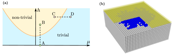
In this paper, we instead choose to explore an alternative route. We consider an inhomogeneous system but in a constant magnetic Zeeman energy, which would reside on the C–D line in Fig. 1(a). The transition to the topological domain occurs due to a change in the chemical potential . Such a system could be constructed experimentally in many different ways: one option would be to substitute the magnetic atoms in the Co island Ménard et al. (2017) by non-magnetic ones and add a magnetic field parallel to the SC Pb monolayer [Fig. 1(b)]. Another promising approach is to use the versatility offered by 2D van-der-Waals heterostructures Novoselov et al. (2016). A possible way to generate an homogeneous Zeeman exchange energy in the proximity of a superconductor could be engineered by stacking recently synthesized 2D magnetic materials Burch et al. (2018); Gong and Zhang (2019) with a transition metal dichalcogenide (TMD) superconductor such as NbSe2. A non-magnetic island can be obtained by evaporating some alkaline adatoms to enforce charge transfer.
The paper is organized as follows: In Sec. II, we first start with a circular geometry for the nanoflake and derive the dispersive chiral Majorana edge states analytically in the continuum limit. We also discuss the spatial extent of the chiral Majorana modes in the tranverse direction. In Sec. III we compare our results obtained in the continuum limit to exact diagonalization of a tight binding model on a lattice. In Sec. IV, we propose and study a setup in order to measure the chirality of the Majorana edge states using two ferromagnetic tips. Finally, we present a summary of our results and give conclusions in Sec. V.
II Nanoflake with circular geometry
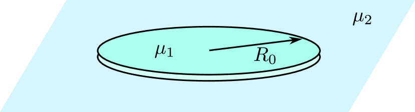
We begin by considering a nanoflake with a circular symmetry as depicted in Fig. 2. For simplification and without a loss of generality, we can also assume a smooth boundary of the nanoflake. Keeping in mind the circular symmetry, the Hamiltonian will commute with the th component of the total angular momentum operator . We may then find the energies of the bound state wave functions localized at the edge of the nanoflake in terms of the quantum numbers. This method allows us to determine the existence of chiral subgap states within our system, and has successfully been used in the studies of other 2D systems with circular symmetry such as graphene Asmar and Ulloa (2014).
Thus, the real-space normal state Hamiltonian has the form,
| (1) |
where (for ) are the Pauli matrices acting in spin space. Here, the system is 2D with , and the chemical potential is given by,
| (2) |
We may also define the discontinuity at the boundary, see Fig. 2. In other words, corresponds to the spatial variation of the chemical potential induced by the nanoflake. The BdG Hamiltonian may then be expressed as,
where is the Nambu spinor, with being electron field operators which destroy an electron with spin at location .
Due to the circular symmetry of the nanoflake (or more precisely, the scalar chemical potential ), the BdG Hamiltonian commutes with the th component of the total angular momentum operator . It follows that the Hamiltonian and share the same eigenstates. The eigenstates of , with the half-integer eigenvalues , are given by
| (4) |
To focus on states with small total angular momenta, we take a low-energy approximation and neglect the kinetic energy term in the Hamiltonian Oreg et al. (2010). By writing the and functions in terms of the Modified Bessel Functions of the First and Second Kind, we may then solve for the bound state wave functions localized at . The details of this approach can be found in the Supplemental Material (SM) 111See Supplemental Material at [URL will be inserted by the publisher] for details of the analytical calculations and additional numerical results for the nanoflake with irregular shape. In the second case, the numerical results for different sets of values and are presented., and the resulting wave functions have the form:
| (5) |
where
| (6) |
and
| (7) |
Here and are the Modified Bessel Functions of the first and second kind, respectively. The , , and parameters along with the normalizations are derived within the SM Note (1), while the radial momenta which control the spatial extent of the bound states wave functions are given by
| (8) |
where and . For each of the bound states localized at , the total radial spatial extent of the wave functions are thus determined by
| (9) |
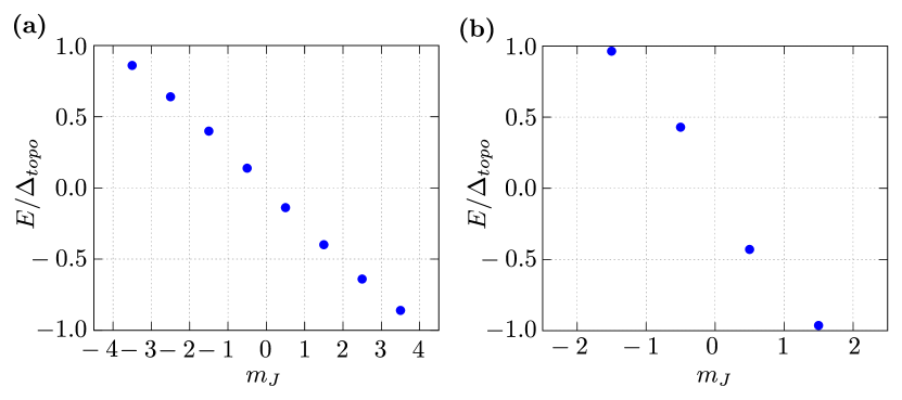
Results are presented for two different sets of parameters:
(a) meV, meV, meV, and
(b) meV, meV, meV.
We take nm and meVnm.
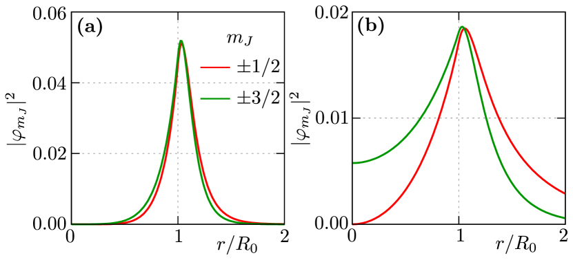
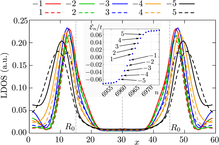
The energy spectrum of these bound states vs the quantum numbers is presented in Fig. 3, while the spatial profile of the wave functions is given in Fig. 4 for two different characteristic sets of parameters. The number of in-gap states is quantized due to the finite perimeter of the nanoflake and their energy spacing depends on intrinsic parameters. In the first set of parameters, we find 8 in-gap states while we have 4 in-gap states in the second set. We choose the strength of the Zeeman field such that the topological gap,
| (10) |
is equal both inside and outside the nanoflake. From our first set of data we obtain meV, while for our second set we obtain meV. The existence of only one branch of states in the topological gap signals that they are chiral (here left handed). This in turn supports the hypothesis of a phase separation in space with a chiral Majorana edge state circulating around the nanoflake.
We also note that these dispersive states are not perfectly linear, but instead exhibit a slight cubic behavior. Comparing both set of parameters, we see that the larger the discontinuity , the more localized the edge states are. This behavior is expected; indeed, the in-gap Majorana states are pinned at the domain wall which is controlled by the spatial variation of the chemical potential.
III Tight binding formulation
In order to confirm our calculations performed in the continuum limit and to go beyond the circular symmetry assumption for a nanoflake, we have also performed numerical calculations on a lattice based on a tight binding description. Our system can be described by the following tight binding Hamiltonian,
| (11) |
The first term corresponds to a free particle on a 2D square lattice,
| (12) |
Here is the hopping integral between nearest neighbor sites 222In the case of an homogeneous 2D system, this gives a dispersion relation . Then, the minimal available energy is equal to ., is the chemical potential (calculated from the bottom of the band), while can be regarded either as a genuine Zeeman energy or as a magnetic exchange energy depending on the situation under consideration. In all cases, we treat it as an effective magnetic field in what follows. The second term describes the in-plane SOC,
| (13) |
where vectors stand for the locations of the neighbors of the i-th site, while is the vector with the Pauli matrices being its components. A SC gap can be induced in the layer through the proximity effect—this process is described through the third term by the BCS-like form,
| (14) |
The last term in Eq. (11) denotes the influence of the nanoflake at the particle distribution,
| (15) |
We assume that every atom comprising the nanoflake changes the energy levels of the rest of the sites, i.e., we assume a long-range impurity potential given by , where the summation is carried out over all adatoms in a given configuration Maśka et al. (2007). Here, denotes the characteristic length of decay of the impurity potential.
The Hamiltonian can be diagonalized by the unitary transformation,
| (16) |
which leads to the Bogoliubov–de Gennes (BdG) equations De Gennes (1999) of the form
| (17) |
with eigenvectors . Here
| (22) |
is the Hamiltonian in the matrix form, with matrix elements as the kinetic term, describing the SC correlations, and standing for the matrix representation of the spin–orbit coupling. More details of this method can be found e.g. in Ref. Balatsky et al. (2006).
III.1 Numerical results
We report the calculations on a square lattice with periodic boundary conditions (PBC). Omitting generality, in the calculations presented in this subsection we use a nanoflake with a circular shape and a radius , which covers about 20% of the total area. We present results for a nanoflake characterized by and . In subsequent calculations, we take , , and . If not mentioned explicitly in the text, the value of the magnetic Zeeman field was chosen so that the boundary between the trivial and non–trivial phases remains in the center of the artificial domain wall (typically ).
III.1.1 Density of states
From the solutions of the BdG equations, we first calculate the local density of states (LDOS) Matsui et al. (2003),
| (23) |
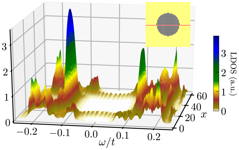
where we replace the Dirac function by a Lorentzian, , with a small broadening . Figure 5 shows an example of the LDOS for a chosen path (along the nanoflake with ). The non–trivial domain is separated from the trivial phase by in-gap states strongly localized along the edge of the nanoflake (cf. Fig. 6). The domain wall is visible in the form of two sets of LDOS peaks with oscillating intensity near the , which are a result of the discrete nature of the in-gap state’s spectrum. The LDOS in our system does not exhibit an “X”–shape crossing through the energy gap around the nanoflake edge, in contrast to the results presented in Refs. Ménard et al. (2017); Björnson and Black-Schaffer (2018). Nevertheless, our results are in agreement with experimental results presented in Ref. Palacio-Morales et al. (2019). In consequence, we do not observe the two-ring localization like in Refs. Ménard et al. (2017); Björnson and Black-Schaffer (2018) but a one-ring structure along the nanoflake boundary like in Ref. Palacio-Morales et al. (2019).
The localization of the in-gap states is shown Fig. 6. As we can see, the edge states are localized around the nanoflake at the border between the trivial and topological phases. All states create localized states with a circular shape of the same radius (equal approximately to ), while the radius of the nanoflake is equal (shown by doted-dashed line). The difference of these results with respect to the ones discussed in the continuum limit is a consequence of the smearing of the domain wall given by .
The total density of states (DOS) of the system per site is given by a summation of the LDOS over the whole 2D space, i.e., . Here, we can separate the sum into three different terms
| (24) |
a contribution from the sites belonging to nanoflake, a contribution from the domain wall (DW), and a contribution from the bulk states [cf. inset in Fig. 7(b)]. As in Ref. Björnson and Black-Schaffer (2015), we can define the functions in order to classify the states in real space. These functions are equal to when a site belongs to a given region, and otherwise. We assume that the NF (bulk) region is located in sites where the nanoflake changes (does not change) the chemical potential significantly, i.e., (). Otherwise, we treat the site as a part of the DW region, i.e., when . These conditions can be smoothed arbitrarily without changing the results qualitatively (see Fig. S6 and Fig. S7 in the SM Note (1)).
We use this recipe to present the partial density of states (PDOS), which is defined as follows
| (25) |
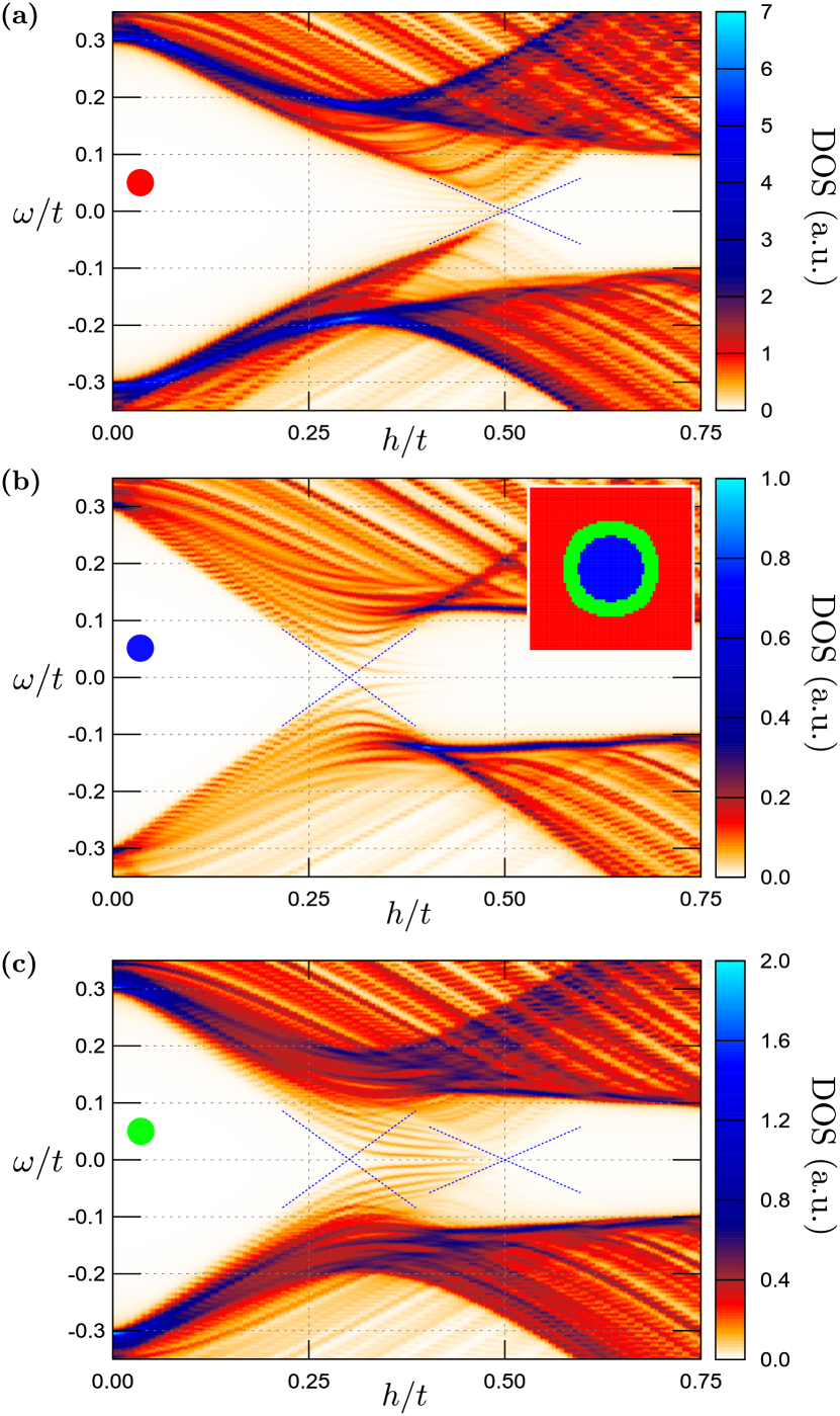
The contribution of the bulk (NF) presented in Fig. 7(a) [Fig. 7(b)], looks like the familiar DOS of a pure 2D Rashba spin-orbit coupled superconductor, in which the gap closing is followed by a reopening of the topological gap. Dashed blue lines serve as a guide to the eye, showing the linear continuation of the last negative and first positive eigenvalue. The value of the magnetic field for which these dashed lines cross zero energy indicate the phase transition from trivial to non–trivial phase.
For effective fields larger than this crossing point, in both cases we observe a topological gap opening around . Contrary to this, the DW PDOS [Fig. 7(c)] ressembles a non–trivial 2D system with egdes Kobiałka et al. (2019). Between critical fields for bulk and NF regions (dashed blue lines crossing the Fermi level), we observe the in-gap states associated only with DW, which confirms the existence of bound states localized along the DW. Additionally, with the increase of , the contribution of these states to the total DOS is shifted from the DW to bulk region (cf. Fig. S8 in the SM Note (1)).
III.1.2 Non–trivial topological domains and topological phase diagram
A magnetic field, , leads to a closing of the trivial SC gap and reopening of a new non–trivial topological gap. This occurs at the critical energy Sato and Fujimoto (2009); Sato et al. (2009, 2010) ( for our choice of parameters). In our system, the value of the chemical potential varies from site to site i.e., . This non-homogeneity can lead to a situation in which the above condition is met only locally Liu and Hu (2012); Liu and Drummond (2012); Ptok et al. (2018). We can therefore construct a space dependent indicator Zhou et al. (2019) that describes the spatial distribution of the non–trivial topological phase,
| (26) |
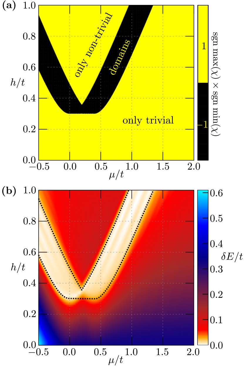
Thus, positive (negative) sign of indicates the topologically trivial (non–trivial) phase. Indeed, from the analysis of under an increase of the magnetic field (see Fig. S9 in the SM Note (1)), we find that the non-trivial phase exists in the system when .
From the above analysis, it follows that the spatial dependence of the indicator gives a correct information about the emergence of the non–trivial topological domain inside the nanoflake. Using this condition, we construct a topological phase diagram in the two-parameter space defined by the chemical potential and the effective magnetic field shown in Fig. 8(a).
First, we recall that the trivial and non–trivial topological phases are separated by a parabolic boundary in the homogeneous system. In our system, the nanoflake introduces a non-homogeneity in to the system, thus the boundary splits due to the existence of two regions in space where topological phases can emerge. As a consequence, the boundary in the phase diagram evolves into a stripe, whose width is given by . Thus, in the limit (homogeneous system without any nanoflake), the “stripe” would narrow down into a line , as seen in Fig. 1.
Second, the region of the stripe separating the phases coincides with the value of the gap , calculated as the energy difference between the eigenvalues closest to Fermi level [Fig. 8(b)]. The existence of a non–trivial domain in the system is a result of the occurrence of in-gap states with exponentially small eigenenergies (described by ).
III.1.3 Bond current
When the system has boundaries Röntynen and Ojanen (2015); Kobiałka et al. (2019), or if artificial barriers are introduced Ptok et al. (2018); Kobiałka and Ptok (2019), in-gap states localize on the edges of the system. The in-gap states are localized in a collection of preferable locations, independently of the broadening of domain wall. These well–localized in-gap states provide a contribution to the bond current which can be expressed as the local charge flow and is obtained from the Heisenberg equation Pershoguba et al. (2015); Li et al. (2016); Björnson et al. (2015),
| (27) |
The current vector field can be represented as a sum of the spin-dependent currents, , where can be expressed by the BdG eigenvectors Björnson et al. (2015); Głodzik and Domański (2020).
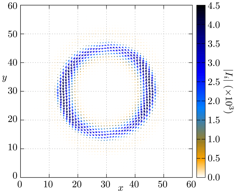
In Fig. 9, we present the real space map of the bond current. Color of the arrows denotes their magnitude . Once again, the width of the domain wall (controlled by ) is reflected by an observable, however, this time it is through the area in which there is a significant flow of charge (cf. Fig. S3 in the SM Note (1)). These low energy modes bear a close resemblance to the surface states of three-dimensional (3D) topological insulators (TIs) Hasan and Kane (2010); Chang and Li (2016). Due to the SOC induced band inversion and bulk-boundary correspondence, the 2D surface of a TI hosts metallic states which disperse through the band gap. Generally, band inversion is a result of the non–trivial phase transition, but here“surface states” are limited to the boundary of the nanoflake, which serves as an edge of the system. The current vector field presented in Fig. 9 is the sum of the contributions of the spin- and spin- current.
Due to the breaking of time reversal symmetry, the spin- component dominates and thus resembles the “quasi-helical” situation described in Ref. Ménard et al. (2017). It is worth noting that a magnetic impurity or a ferromagnetic island proximity–coupled to a SOC superconductor will exhibit a finite spin polarization, thus giving rise to persistent currents Pershoguba et al. (2015); Björnson et al. (2015); Li et al. (2016) as a result of the magnetoelectric effect. This type of bond current along the nanoflake can be observed experimentally, e.g. in the differential conductance measurements Drozdov et al. (2014); Palacio-Morales et al. (2019).
III.2 Numerical results for irregular nanoflake
In order to go beyond the circular limit discussed in previous paragraphs, we locate the substituted atoms at random sites of the lattice as nearest neighbors of an initial atom, located at the center of the surface. This method results in a nanoflake with rugged boundary (cf. Fig. 1) between the substituted (blue) and substrate (gray) atoms, which is similar to experimental setups Ménard et al. (2017); Palacio-Morales et al. (2019). However, artificial construction of nanoflakes could be characterized by a more regular shape too. In practice, in the SM Note (1), we show that the main properties of the system do not depend qualitatively on the shape of the nanoflake. Therefore, all properties described before remain when the flake becomes irregular.
IV Proposal to experimentally measure the chirality using Scanning tunneling Microscopy
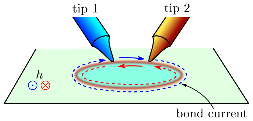
Our experimental proposal is based on the double-tip measurement technique Shiraki et al. (2001); Kolmer et al. (2017); Voigtländer et al. (2018). The in-gap edge states localized around the nanoflake can give a nonlocal response between two spatially separated tips, which is schematically shown in Fig. 10. Similar transconductance technique was successfully used to measure an in-gap surface band Kolmer et al. (2019).
We performed the calculation of the local and non-local differential conductance using the Kwant Groth et al. (2014) code to numerically obtain the scattering matrix Lesovik and Sadovskyy (2011); Akhmerov et al. (2011); Fulga et al. (2011):
| (32) |
Here, is the block of the scattering amplitudes of incident particles of type in tip to particles of type in tip . Then, the differential conductance matrix is given as Rosdahl et al. (2018):
| (33) |
where is the current entering terminal from the scattering region and is the voltage applied to the terminal , and is the number of electron modes at energy in terminal . Finally, the energy transmission is:
| (34) |
The nonlocal response is constituted by two processes:
(i) a
direct electron transfer between the leads and (ii) the crossed Andreev reflection (CAR) of an electron from one tip into a hole in the second tip Byers and Flatté (1995); Deutscher and Feinberg (2000).
In typical cases, the CAR contribution dominates the electron transfer Falci et al. (2001); Beckmann et al. (2004) and such processes is responsible for the Cooper pair splitter Herrmann et al. (2010).
Here, we show that this technique has a potential application in measuring the chirality of the edge state.
In order to achieve this goal, we suggest the use of two ferromagnetic tips described by the Hamiltonian:
| (35) |
where is the dispersion relation of the free electrons in the tips, while is the magnetization of the tip. We assume that the tips have opposite magnetization, i.e. . The tips are separated from the plane of the system by the barrier potential. We assume a system like that shown schematically in Fig. 10, i.e. tips are located exactly above the nanoflake edge, in a non-symmetric position. As a result, a distance between 1st and 2nd tip differs when measured clockwise or counterclockwise (along the edge state channel at the border of the nanoflake).
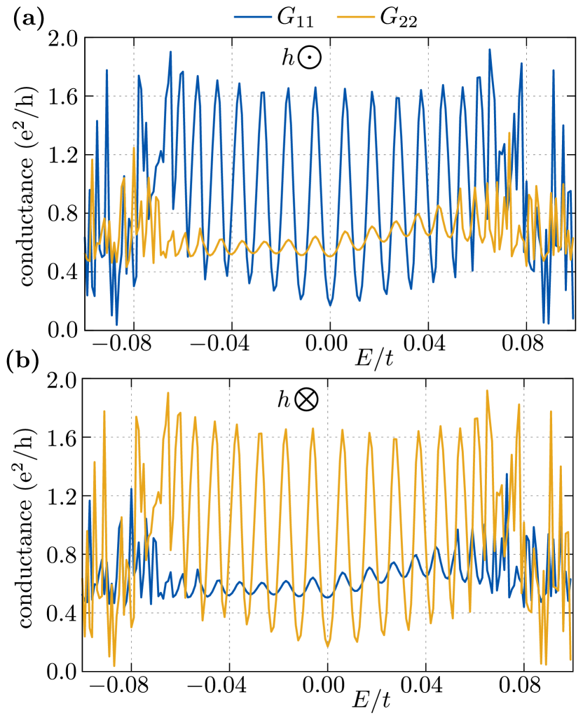
In our system, we can find the local ( and ) as well as non-local ( and ) differential conductance (Fig. 11 and Fig. 12, respectively). The local conductance can be treated as a probe of the existence of states in the system Chen et al. (2017); Zhang et al. (2018). In this sense, each state gives a positive signal in , independently of the direction of the magnetic field (see top and bottom panels in Fig. 11). As we can see, in our case we observe several in-gap states. Due to the use of ferromagnetic tips we observe non-equality of and (blue and red lines, respectively).
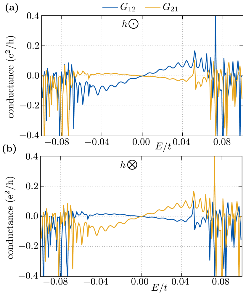
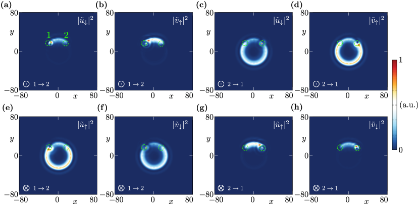
The non-local conductances and (Fig. 12) describe different situations. In order for CAR processes to occur, electrons from both tips need to have opposite spins to create a Cooper pair and simultaneously eject a hole from the other tip. Due to the applied external magnetic field the incident electrons from the edge bond current would have the same spin as the electrons from the first tip they encounter. The electron with opposite spin should come the other tip (which has opposite magnetization) and emit a hole with the same spin to constitute a CAR process. Thanks to this nonlocal phenomena, we can easily determine the direction of the edge state propagation as the nonlocal conductance coincides with the direction of chiral bond current. Thus, if the sign of magnetic field changes, the direction of the edge state propagation reverts too, becomes due to the spatial symmetry of the system. However, tips are not perfectly magnetized, therefore nonlocal conductance measurement in the direction opposite to the chiral bond current remains nonzero (e.g. for direction of magnetic field). As the edge state bond current is constituted of both spins, particles with spins not aligned with the tip magnetization scatter off the tip (cf. wavefunction localizations in Fig. 13). If the magnetic field is not present in the system, in-gap nonlocal conductance vanishes (not shown), and peaks at the edge of superconducting gap appear Rosdahl et al. (2018). Differences between the absolute value of non-local conductances are the consequence of the non-symmetric position of the tips. The change from negative to positive slope near the gap can be interpreted as a crossover from subgap transport dominated by crossed Andreev reflection to charge imbalance above the gap Kalenkov and Zaikin (2011). Additionally, the non-local conductance strongly depends on a distance between the tips Rosdahl et al. (2018).
To explain the above results, we analyzed the propagating modes in the system (Fig. 13). The nonlocal transport corresponds to situation where incident electron from one tip is transmitted through the edge modes as the chiral mode and is scattered into the second tip. Such propagating modes can be represented in form of wavefunction , where and correspond to its electron- and hole-like component, respectively. Here, is composed mostly of -electron and -hole component Ikegaya et al. (2019). Regions with the non–zero probability of localization correspond to the particle remnants of scattering processes, which distribution coincides with the direction of edge state propagation. As we mentioned above, with relatively small voltage bias, the non-local transport is dominated by CAR processes (which was envisioned by the antiparallel magnetization of and ). In the case of the “positive” magnetic field, we observe propagation from 1st to 2nd tip in clockwise direction [Fig. 13, panels (a) and (b)], for both electron and hole component of the wavefunction. Then, if we check the mode propagation from 2nd to 1st tip [Fig. 13, panels (c) and (d)], we can see that the chirality of the propagating modes is preserved and clockwise. In the case of the magnetic field with opposite direction, we observe modes propagating in opposite direction as previously mentioned (bottom panels in Fig. 13). Without any surprise, mode propagation direction in this case is also preserved.
Summarizing, the non-local conductance is not just a fingerprint of the existence of the chiral mode Ikegaya et al. (2019), but also a tool to measure its chirality.
V Summary and conclusions
Recent experimental results have presented the possibility of the emergence of non–trivial topological phases in magnetic nanostructures coupled to superconducting substrates Ménard et al. (2017); Palacio-Morales et al. (2019).
In this paper, we have explored the artificial implementation of topological phase transitions induced by the local modification of the chemical potential. In this respect, we performed analytic calculations valid in the continuum limit in the case of a nanoflake with a circular geometry and found the spectrum of the system as a function of the total angular momentum. We have also studied how the transverse spatial extent of the wave function of the chiral Majorana state localized around the nanoflake depends upon the system parameters. We then performed similar calculations for a finite size geometry using a tight binding formulation. In-gap states correspond to prominent peaks in the LDOS only in a distinct region of space, identified as the domain wall, which should be observed relatively simply through STM experiments. We have introduced a real space indicator, which locally characterizes the topological phase. Indeed, for a few sets of parameters, results obtained from this indicator were in agreement with those obtained in the continuum limit. In the case analyzed here, the effective magnetic field leads to the realization of a non–trivial phase only in distinct regions of the system, creating a non–trivial superconducting dome surrounded by a trivial superconducting phase. This phase separation could be observed through the measurement of a bond chiral current, which is connected to the existence of strongly localized in-gap states. We have shown that this current circulates around the nanoflake. Additionally, with the help of the indicator, we have found the topological phase diagram of the system. We have shown that an artificial phase separation can be induced for a finite range of effective magnetic field. The boundary of this phase separation is strongly related to the effective magnetic field, which determines the transition between trivial to non–trivial phases
In the last part of our work, we have proposed an experimental method to measure the chiraliy of the edge states, based on a double-tip measurement of the non-local differential conductivity. We have found that the non-local transport properties between the two tips allow one to determine the chirality of the edge state. Although challenging, this type of experiment should be accessible with the present technology.
Acknowledgements.
We would like to thank Tristan Cren for interesting discussions. This work was supported by the National Science Centre (NCN, Poland) under grants Nos.: 2017/24/C/ST3/00276 (A.P.), 2017/27/N/ST3/01762 (S.G.), 2018/31/N/ST3/01746 (A.K.), 2016/23/B/ST3/00839 (A.M.O.), and 2017/25/B/ST3/02586 (P.P.). A. M. Oleś is grateful for the Alexander von Humboldt Foundation Fellowship (Humboldt-Forschungspreis). AP appreciate also founding in the frame of scholarships of the Minister of Science and Higher Education (Poland) for outstanding young scientists (2019 edition, no. 818/STYP/14/2019).References
- Kitaev (2003) A.Yu. Kitaev, “Fault-tolerant quantum computation by anyons,” Ann. Physics 303, 2 (2003).
- Nayak et al. (2008) Ch. Nayak, S. H. Simon, A. Stern, M. Freedman, and S. Das Sarma, “Non-Abelian anyons and topological quantum computation,” Rev. Mod. Phys. 80, 1083 (2008).
- Alicea et al. (2011) J. Alicea, Y. Oreg, G. Refael, F. von Oppen, and M. P. A. Fisher, “Non-Abelian statistics and topological quantum information processing in 1d wire networks,” Nat. Phys. 7, 412 (2011).
- Alicea (2012) J. Alicea, “New directions in the pursuit of Majorana fermions in solid state systems,” Rep. Prog. Phys. 75, 076501 (2012).
- Aasen et al. (2016) D. Aasen, M. Hell, R. V. Mishmash, A. Higginbotham, J. Danon, M. Leijnse, T. S. Jespersen, J. A. Folk, Ch. M. Marcus, K.n Flensberg, and J. Alicea, “Milestones toward Majorana-based quantum computing,” Phys. Rev. X 6, 031016 (2016).
- Lian et al. (2018) B. Lian, X.-Q. Sun, A. Vaezi, X.-L. Qi, and S.-Ch. Zhang, “Topological quantum computation based on chiral Majorana fermions,” Proc. Natl. Acad. Sci. U.S.A. 115, 10938 (2018).
- Qi and Zhang (2011) X.-L. Qi and S.-Ch. Zhang, “Topological insulators and superconductors,” Rev. Mod. Phys. 83, 1057 (2011).
- He et al. (2017) Q. L. He, L. Pan, A. L. Stern, E. C. Burks, X. Che, G. Yin, J. Wang, B. Lian, Q. Zhou, E. S. Choi, K. Murata, X. Kou, Z. Chen, T. Nie, Q. Shao, Y. Fan, S.-Ch. Zhang, K. Liu, J. Xia, and K. L. Wang, “Chiral Majorana fermion modes in a quantum anomalous Hall insulator–superconductor structure,” Science 357, 294 (2017).
- Ménard et al. (2017) G. C. Ménard, S. Guissart, Ch. Brun, R. T. Leriche, M. Trif, F. Debontridder, D. Demaille, D. Roditchev, P. Simon, and T. Cren, “Two-dimensional topological superconductivity in Pb/Co/Si(111),” Nat. Commun. 8, 2040 (2017).
- Drost et al. (2017) R. Drost, T. Ojanen, A. Harju, and P. Liljeroth, “Topological states in engineered atomic lattices,” Nat. Phys. 13, 668 (2017).
- Kim et al. (2018) H. Kim, A. Palacio-Morales, T. Posske, L. Rózsa, K. Palotás, L. Szunyogh, M. Thorwart, and R. Wiesendanger, “Toward tailoring Majorana bound states in artificially constructed magnetic atom chains on elemental superconductors,” Sci. Adv. 4, eaar5251 (2018).
- Kamlapure et al. (2018) A. Kamlapure, L. Cornils, J. Wiebe, and R. Wiesendanger, “Engineering the spin couplings in atomically crafted spin chains on an elemental superconductor,” Nat. Commun. 9, 3253 (2018).
- Ménard et al. (2019) G. C. Ménard, A. Mesaros, Ch. Brun, F. Debontridder, D. Roditchev, P. Simon, and T. Cren, “Isolated pairs of Majorana zero modes in a disordered superconducting lead monolayer,” Nat. Commun. 10, 2587 (2019).
- Palacio-Morales et al. (2019) A. Palacio-Morales, E. Mascot, S. Cocklin, H. Kim, S. Rachel, D. K. Morr, and R. Wiesendanger, “Atomic-scale interface engineering of Majorana edge modes in a 2D magnet-superconductor hybrid system,” Sci. Adv. 5, eaav6600 (2019).
- Sato and Fujimoto (2009) M. Sato and S. Fujimoto, “Topological phases of noncentrosymmetric superconductors: Edge states, Majorana fermions, and non-Abelian statistics,” Phys. Rev. B 79, 094504 (2009).
- Sato et al. (2009) M. Sato, Y. Takahashi, and S. Fujimoto, “Non-Abelian topological order in -wave superfluids of ultracold fermionic atoms,” Phys. Rev. Lett. 103, 020401 (2009).
- Sato et al. (2010) M. Sato, Y. Takahashi, and S. Fujimoto, “Non-Abelian topological orders and Majorana fermions in spin-singlet superconductors,” Phys. Rev. B 82, 134521 (2010).
- Novoselov et al. (2016) K. S. Novoselov, A. Mishchenko, A. Carvalho, and A. H. Castro Neto, “2D materials and van der Waals heterostructures,” Science 353, aac9439 (2016).
- Burch et al. (2018) K. S. Burch, D. Mandrus, and J.-G. Park, “Magnetism in two-dimensional van der Waals materials,” Nature 563, 47 (2018).
- Gong and Zhang (2019) Ch. Gong and X. Zhang, “Two-dimensional magnetic crystals and emergent heterostructure devices,” Science 363, eaav4450 (2019).
- Asmar and Ulloa (2014) M. M. Asmar and S. E. Ulloa, “Spin-orbit interaction and isotropic electronic transport in graphene,” Phys. Rev. Lett. 112, 136602 (2014).
- Oreg et al. (2010) Y. Oreg, G. Refael, and F. von Oppen, “Helical liquids and Majorana bound states in quantum wires,” Phys. Rev. Lett. 105, 177002 (2010).
- Note (1) See Supplemental Material at [URL will be inserted by the publisher] for details of the analytical calculations and additional numerical results for the nanoflake with irregular shape. In the second case, the numerical results for different sets of values and are presented.
- Note (2) In the case of an homogeneous 2D system, this gives a dispersion relation . Then, the minimal available energy is equal to .
- Maśka et al. (2007) M. M. Maśka, Ż. Śledź, K. Czajka, and M. Mierzejewski, “Inhomogeneity-induced enhancement of the pairing interaction in cuprate superconductors,” Phys. Rev. Lett. 99, 147006 (2007).
- De Gennes (1999) P. G. De Gennes, Superconductivity Of Metals And Alloys, Advanced Books Classics Series (Westview Press, 1999).
- Balatsky et al. (2006) A. V. Balatsky, I. Vekhter, and J.-X. Zhu, “Impurity-induced states in conventional and unconventional superconductors,” Rev. Mod. Phys. 78, 373 (2006).
- Matsui et al. (2003) H. Matsui, T. Sato, T. Takahashi, S.-C. Wang, H.-B. Yang, H. Ding, T. Fujii, T. Watanabe, and A. Matsuda, “BCS-like bogoliubov quasiparticles in high-Tc superconductors observed by angle-resolved photoemission spectroscopy,” Phys. Rev. Lett. 90, 217002 (2003).
- Björnson and Black-Schaffer (2018) K. Björnson and A. M. Black-Schaffer, “Probing chiral edge states in topological superconductors through spin-polarized local density of state measurements,” Phys. Rev. B 97, 140504(R) (2018).
- Björnson and Black-Schaffer (2015) K. Björnson and A. M. Black-Schaffer, “Probing vortex Majorana fermions and topology in semiconductor/superconductor heterostructures,” Phys. Rev. B 91, 214514 (2015).
- Kobiałka et al. (2019) A. Kobiałka, T. Domański, and A. Ptok, “Delocalisation of Majorana quasiparticles in plaquette–nanowire hybrid system,” Sci. Rep. 9, 12933 (2019).
- Liu and Hu (2012) X.-J. Liu and H. Hu, “Topological superfluid in one-dimensional spin-orbit-coupled atomic Fermi gases,” Phys. Rev. A 85, 033622 (2012).
- Liu and Drummond (2012) X.-J. Liu and P. D. Drummond, “Manipulating Majorana fermions in one-dimensional spin-orbit-coupled atomic Fermi gases,” Phys. Rev. A 86, 035602 (2012).
- Ptok et al. (2018) A. Ptok, A. Cichy, and T. Domański, “Quantum engineering of Majorana quasiparticles in one-dimensional optical lattices,” J. Phys.: Condens. Matter 30, 355602 (2018).
- Zhou et al. (2019) T. Zhou, N. Mohanta, J. E. Han, A. Matos-Abiague, and I. Žutić, “Tunable magnetic textures in spin valves: From spintronics to Majorana bound states,” Phys. Rev. B 99, 134505 (2019).
- Röntynen and Ojanen (2015) J. Röntynen and T. Ojanen, “Topological superconductivity and high Chern numbers in 2D ferromagnetic Shiba lattices,” Phys. Rev. Lett. 114, 236803 (2015).
- Kobiałka and Ptok (2019) A. Kobiałka and A. Ptok, “Electrostatic formation of the majorana quasiparticles in the quantum dot-nanoring structure,” J. Phys.: Condens. Matter 31, 185302 (2019).
- Pershoguba et al. (2015) S. S. Pershoguba, K. Björnson, A. M. Black-Schaffer, and A. V. Balatsky, “Currents induced by magnetic impurities in superconductors with spin-orbit coupling,” Phys. Rev. Lett. 115, 116602 (2015).
- Li et al. (2016) J. Li, T. Neupert, Z. Wang, A. H. MacDonald, A. Yazdani, and B. A. Bernevig, “Two-dimensional chiral topological superconductivity in Shiba lattices,” Nat. Commun. 7, 12297 (2016).
- Björnson et al. (2015) K. Björnson, S. S. Pershoguba, A. V. Balatsky, and A. M. Black-Schaffer, “Spin-polarized edge currents and Majorana fermions in one- and two-dimensional topological superconductors,” Phys. Rev. B 92, 214501 (2015).
- Głodzik and Domański (2020) Sz. Głodzik and T. Domański, “In-gap states of magnetic impurity in quantum spin Hall insulator proximitized to a superconductor,” J. Phys.: Condens. Matter 32, 235501 (2020).
- Hasan and Kane (2010) M. Z. Hasan and C. L. Kane, “Colloquium: Topological insulators,” Rev. Mod. Phys. 82, 3045 (2010).
- Chang and Li (2016) C.-Z. Chang and M. Li, “Quantum anomalous Hall effect in time-reversal-symmetry breaking topological insulators,” J. Phys.: Condens. Matter 28, 123002 (2016).
- Drozdov et al. (2014) I. K. Drozdov, A. Alexandradinata, S. Jeon, S. Nadj-Perge, H. Ji, R. J. Cava, B. A. Bernevig, and A. Yazdani, “One-dimensional topological edge states of bismuth bilayers,” Nat. Phys. 10, 664 (2014).
- Shiraki et al. (2001) I. Shiraki, F. Tanabe, R. Hobara, T. Nagao, and S. Hasegawa, “Independently driven four-tip probes for conductivity measurements in ultrahigh vacuum,” Surf. Sci. 493, 633 (2001).
- Kolmer et al. (2017) M. Kolmer, P. Olszowski, R. Zuzak, Sz. Godlewski, Ch.n Joachim, and M. Szymonski, “Two-probe STM experiments at the atomic level,” J. Phys.: Condens. Matter 29, 444004 (2017).
- Voigtländer et al. (2018) B. Voigtländer, V. Cherepanov, S. Korte, A. Leis, D. Cuma, S. Just, and F. Lüpke, “Invited review article: Multi-tip scanning tunneling microscopy: Experimental techniques and data analysis,” Rev. Sci. Instrum. 89, 101101 (2018).
- Kolmer et al. (2019) M. Kolmer, P. Brandimarte, J. Lis, R. Zuzak, Sz. Godlewski, H. Kawai, A. Garcia-Lekue, N. Lorente, T. Frederiksen, Ch. Joachim, D. Sanchez-Portal, and M. Szymonski, “Electronic transport in planar atomic-scale structures measured by two-probe scanning tunneling spectroscopy,” Nat. Commun. 10, 1573 (2019).
- Groth et al. (2014) Ch. W. Groth, M. Wimmer, A. R. Akhmerov, and X. Waintal, “Kwant: a software package for quantum transport,” New J. Phys. 16, 063065 (2014).
- Lesovik and Sadovskyy (2011) G. B. Lesovik and I. A. Sadovskyy, “Scattering matrix approach to the description of quantum electron transport,” Phys.-Usp. 54, 1007 (2011).
- Akhmerov et al. (2011) A. R. Akhmerov, J. P. Dahlhaus, F. Hassler, M. Wimmer, and C. W. J. Beenakker, “Quantized conductance at the Majorana phase transition in a disordered superconducting wire,” Phys. Rev. Lett. 106, 057001 (2011).
- Fulga et al. (2011) I. C. Fulga, F. Hassler, A. R. Akhmerov, and C. W. J. Beenakker, “Scattering formula for the topological quantum number of a disordered multimode wire,” Phys. Rev. B 83, 155429 (2011).
- Rosdahl et al. (2018) T. Ö. Rosdahl, A. Vuik, M. Kjaergaard, and A. R. Akhmerov, “Andreev rectifier: A nonlocal conductance signature of topological phase transitions,” Phys. Rev. B 97, 045421 (2018).
- Byers and Flatté (1995) J. M. Byers and M. E. Flatté, “Probing spatial correlations with nanoscale two-contact tunneling,” Phys. Rev. Lett. 74, 306 (1995).
- Deutscher and Feinberg (2000) G. Deutscher and D. Feinberg, “Coupling superconducting-ferromagnetic point contacts by Andreev reflections,” Appl. Phys. Lett. 76, 487 (2000).
- Falci et al. (2001) G Falci, D Feinberg, and F. W. J Hekking, “Correlated tunneling into a superconductor in a multiprobe hybrid structure,” Europhysics Letters (EPL) 54, 255 (2001).
- Beckmann et al. (2004) D. Beckmann, H. B. Weber, and H. v. Löhneysen, “Evidence for crossed Andreev reflection in superconductor-ferromagnet hybrid structures,” Phys. Rev. Lett. 93, 197003 (2004).
- Herrmann et al. (2010) L. G. Herrmann, F. Portier, P. Roche, A. Levy Yeyati, T. Kontos, and C. Strunk, “Carbon nanotubes as Cooper-pair beam splitters,” Phys. Rev. Lett. 104, 026801 (2010).
- Chen et al. (2017) J. Chen, P. Yu, J. Stenger, M. Hocevar, D. Car, S. R. Plissard, E. P. A. M. Bakkers, T. D. Stanescu, and S. M. Frolov, “Experimental phase diagram of zero-bias conductance peaks in superconductor/semiconductor nanowire devices,” Sci. Adv. 3, e1701476 (2017).
- Zhang et al. (2018) H. Zhang, Ch.-X. Liu, S. Gazibegovic, D. Xu, J. A. Logan, G. Wang, N. van Loo, J. D. S. Bommer, M. W. A. de Moor, D. Car, R. L. M. Op het Veld, P. J. van Veldhoven, S. Koelling, M. A. Verheijen, M. Pendharkar, D. J. Pennachio, B. Shojaei, J. S. Lee, Ch. J. Palmstrøm, E. P. A. M. Bakkers, S. Das Sarma, and L. P. Kouwenhoven, “Quantized Majorana conductance,” Nature 556, 74 (2018).
- Kalenkov and Zaikin (2011) M. S. Kalenkov and A. D. Zaikin, “Crossed Andreev reflection and spin-resolved non-local electron transport,” in Fundamentals of Superconducting Nanoelectronics, edited by A. Sidorenko (Springer Berlin Heidelberg, Berlin, Heidelberg, 2011) pp. 67–100.
- Ikegaya et al. (2019) S. Ikegaya, Y. Asano, and D. Manske, “Anomalous nonlocal conductance as a fingerprint of chiral Majorana edge states,” Phys. Rev. Lett. 123, 207002 (2019).