Coulomb interactions and effective quantum inertia of charge carriers in a macroscopic conductor
Abstract
We study the low frequency admittance of a quantum Hall bar of size much larger than the electronic coherence length. We find that this macroscopic conductor behaves as an ideal quantum conductor with vanishing longitudinal resistance and purely inductive behavior up to . Using several measurement configurations, we study the dependence of this inductance on the length of the edge channel and on the integer quantum Hall filling factor. The experimental data are well described by a scattering model for edge magnetoplasmons taking into account effective long range Coulomb interactions within the sample. We find that the inductance’s dependence on the filling factor arises predominantly from the effective quantum inertia of charge carriers induced by Coulomb interactions.
pacs:
72.10.-d, 73.23.-b,73.43.-f, 73.43.FjBy demonstrating that macroscopic conductors could exhibit robust d.c. transport properties of quantum origin, the integer quantum Hall effect (IQHE) Klitzing et al. (1980); Halperin (1982); Haug (1993); Weis and von Klitzing (2011); Suddards et al. (2012) has been a major surprise. The importance of this breakthrough for metrology was acknowledged immediately Klitzing et al. (1980) and has lead to the redefinition of the Ohm des Poids et Mesures (1988). The finite frequency response of quantum Hall conductors has been intensively studied by metrologists: the use of an a.c. bridge at finite frequency revealed departure of the Hall resistance at from the expected value Jeckelmann and Jeanneret (2001); Ahlers et al. (2009); Delahaye (1995); Chua et al. (1999); Schurr et al. (2005). It was then attributed to “intrinsic inductances and capacitances” Cage and Jeffrey (1996); Jeanneret et al. (1995). Later, Schurr et al proposed a double shielded sample allowing for a frequency-independent resistance standard Schurr et al. (2011), but these works left open the question of the origin of these capacitances and inductances.
On the other hand, the finite frequency transport properties of quantum coherent conductors, of size smaller than the electron coherence length, are expected to be dominated by quantum effects. For low-dimensional conductors such as carbon nanotubes Burke (2002), or graphene Kang et al. (2018), the inductance is of purely kinetic origin. Small superconducting inductors Annunziata et al. (2010); Luomahaara et al. (2014) now used in space industry Coiffard et al. (2016) are based on the inertia of Cooper pairs. For a quantum coherent conductor, the theory developed by Bűttiker and his collaborators Büttiker et al. (1993); Büttiker (1993); Prêtre et al. (1996) relates the associated or times to the Wigner-Smith time delay for charge carriers scattering across the conductor. These remarkable predictions have been confirmed by the measurement of the finite frequency admittance of quantum Hall R-C Gabelli et al. (2006) and R-L Gabelli et al. (2007); Song et al. (2018) circuits of -size in the range at cryogenic temperatures.
In this letter, we demonstrate that, in the a.c. regime, a long ungated macroscopic quantum Hall bar, of size much larger than the electronic coherence length, exhibits a finite inductance as well as a vanishing longitudinal resistance. Such a purely inductive longitudinal response is expected for quantum conductors with zero backscattering: a kinetic energy cost proportional to the square of the current arises from both the Pauli principle and the linear dispersion relation for electrons close to the Fermi level (see Appendix A). This effective inertia of carriers causes the current response to lag the applied electric field. Here, we identify an inductance of the order of tens of and connect it to an effective velocity along the quantum Hall bar’s edges. Contrary to gated samples, in which is almost independent of the filling factor Gabelli et al. (2007), we show that, because of Coulomb interactions between opposite edges of the sample, depends on in our samples. Using the edge-magnetoplasmon scattering approach combined with a discrete element approach à la Bűttiker, we show that:
| (1) |
for a sample of width . Here, represents the charge density wave velocity along the system of -copropagating chiral edge channels, neglecting Coulomb interactions with the other (counter-propagating) edge channels. In a Büttiker view of the edge channels Büttiker (1988), is the drift velocity of non-interacting electrons at the edge in an effective confining potential and, therefore, it plays the role of an effective Fermi velocity in the 1D linear dispersion relation along the edge Girvin and Yang (2019). In the presence of compressible stripes, which appear for a sufficiently smooth confining potential Chklovskii et al. (1992), it corresponds to the effective velocity of the charge density mode in the system of copropagating edge channels Aleiner and Glazman (1994), taking into account the presence of the incompressible part of the edge channel Han and Thouless (1997). Nevertheless, we denote it by because, in a model of an edge channel without compressible parts, it really would be an electronic drift velocity. Importantly, this velocity deviates from from the classical behavior of the electronic drift velocity because of screening effects, which change the electrostatic potential at the edge as varies.
Here, denotes the effective fine structure constant ( in the vacuum) at filling factor : . The length , which also depends on , is an effective renormalized width of a single edge channel of the order of the width of incompressible edge channels Chklovskii et al. (1992) (see Appendix D)
Our work demonstrates that the purely inductive response of the macroscopic ungated quantum Hall bar reflects the effective quantum inertia of charge carriers renormalized by Coulomb interactions within the sample. Therefore, although electron transport across such a conductor is not coherent, its d.c. and a.c. transport properties are of quantum origin, a fact that ultimately relies on the coherence of edge-magnetoplasmon (EMP) modes propagating along chiral edge channels. EMP coherence has enabled the demonstration of single and double EMP Fabry-Pérot interferometers Hashisaka et al. (2013) as well as of a Mach-Zehnder plasmonic interferometer Hiyama et al. (2015).
Using shallow etching, our samples are processed on an AlGaAs/GaAs heterojunction with the two dimensional electron gas (2DEG) located at the hetero-interface ( beneath the surface) with carrier density and mobility . We have processed a ungated Hall bar which exhibits a sufficiently large kinetic inductance. The sample has no back gate and is glued on a ceramic sample holder to avoid parasitic capacitances. It is placed at the center of a high magnetic field at .
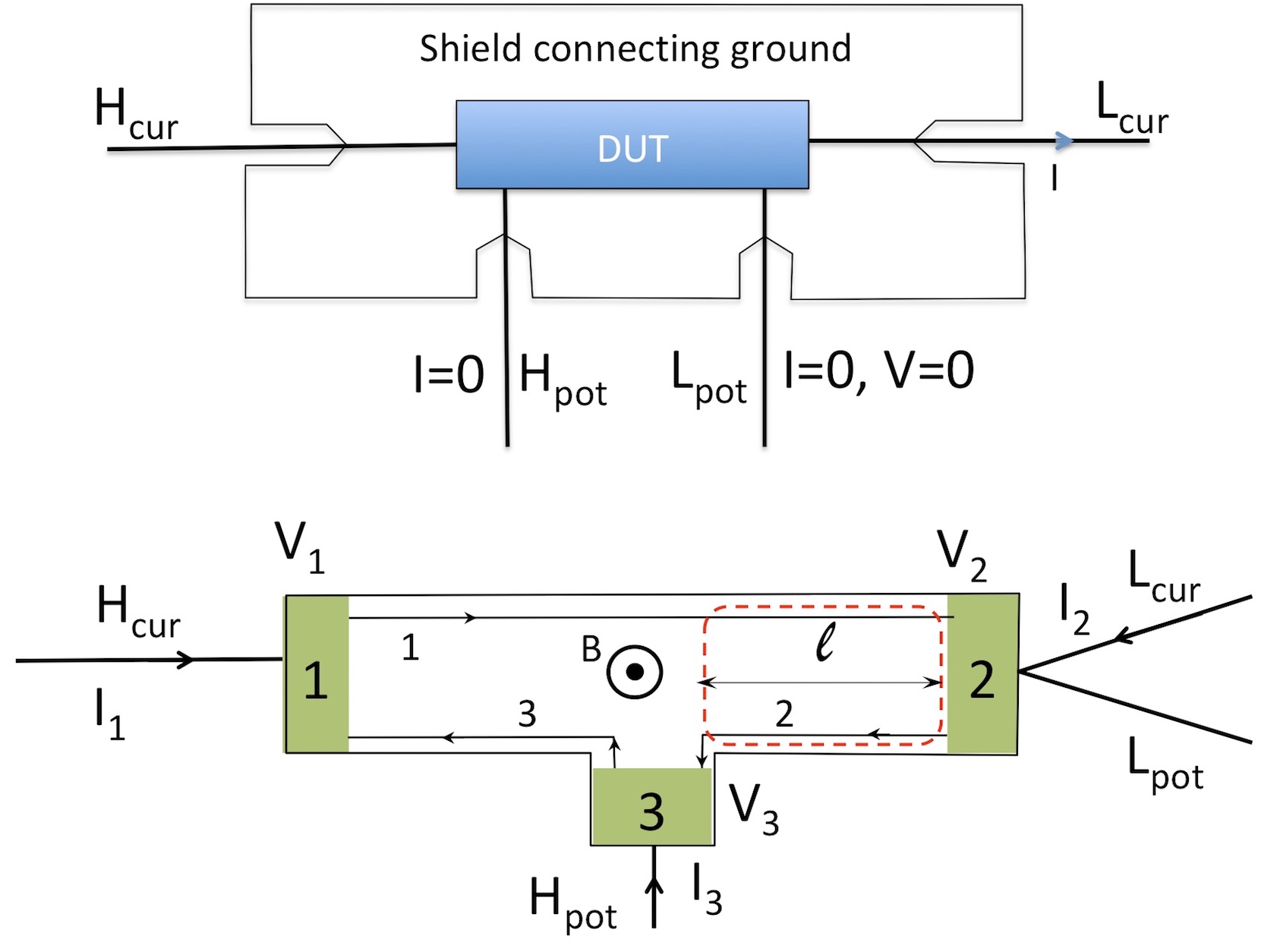
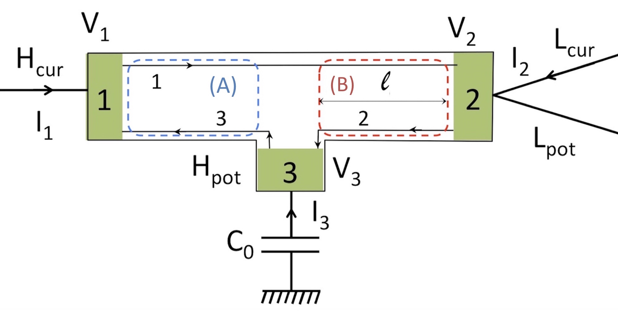
In the measurement setup depicted on Fig. 1-a., the current is injected using ( bias), and measured using . The potential of is measured while and are imposed at . The current intensity ( at ) remains below the breakdown current and currents used in metrology Weis and von Klitzing (2011); Jeckelmann and Jeanneret (2001). For each values of , the resistance and the reactance have been measured for 300 values of the frequency in the range -.
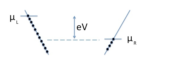
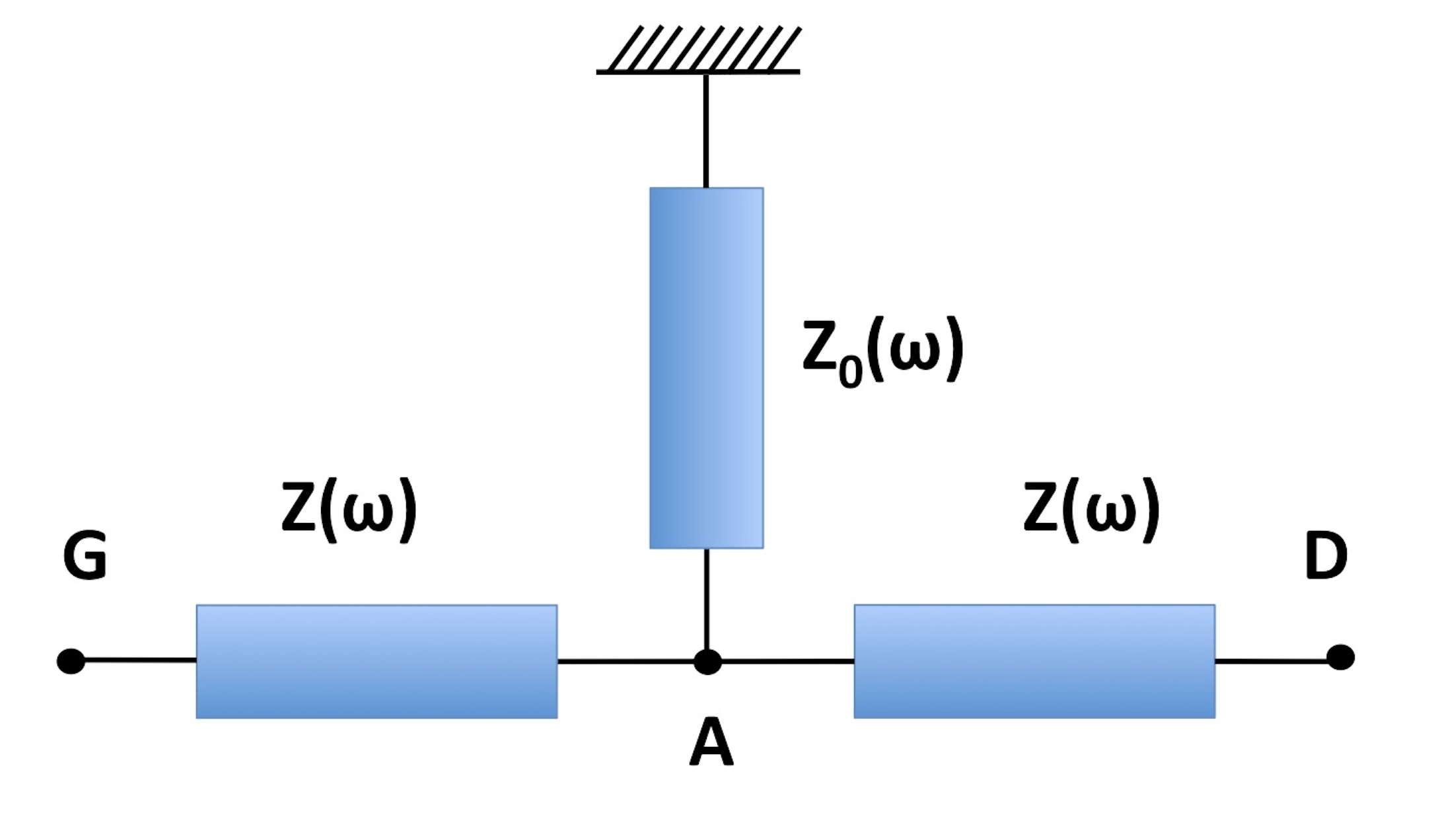
Due to chirality of the quantum Hall transport, an ohmic contact wire-bonded to the sample holder and so to a coaxial cable, generates a leakage current through the cable capacitance if the potential does not vanish Grayson and Fischer (2005); Hernandez et al. (2014). This results in a faulty measurement Desrat et al. (2000); Melcher et al. (2001). For this reason, all results presented here have been carried out at integer filling factors, where the longitudinal resistance vanishes111Here denotes the frequency dependant longitudinal dependence of the quantum Hall bar.. Furthermore, only of the ohmic contacts processed on the sample were wire-bonded onto the sample holder as shown on Fig. 1.b. To measure a zero resistance state, the third contact is inserted along the edge connected to the reference potential. In d.c., one would measure a potential . In a.c., and we measure the frequency dependent impedance . Different configurations and edge channel lengths can be obtained by recabling the contacts and changing the sample side (in this case, the magnetic field orientation must be reversed). We have also wire-bonded a fourth ohmic contact on the same side of the sample to connect to access another edge channel length.
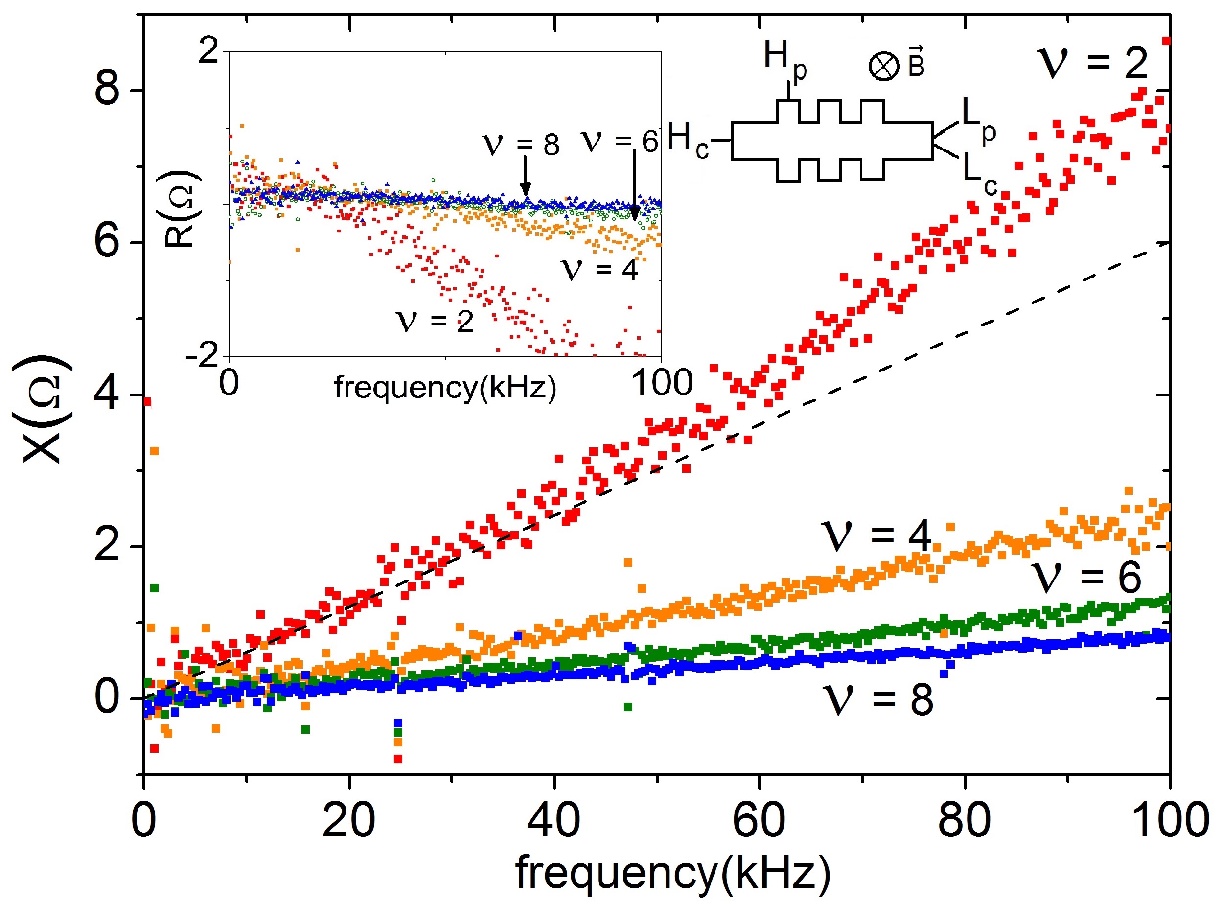
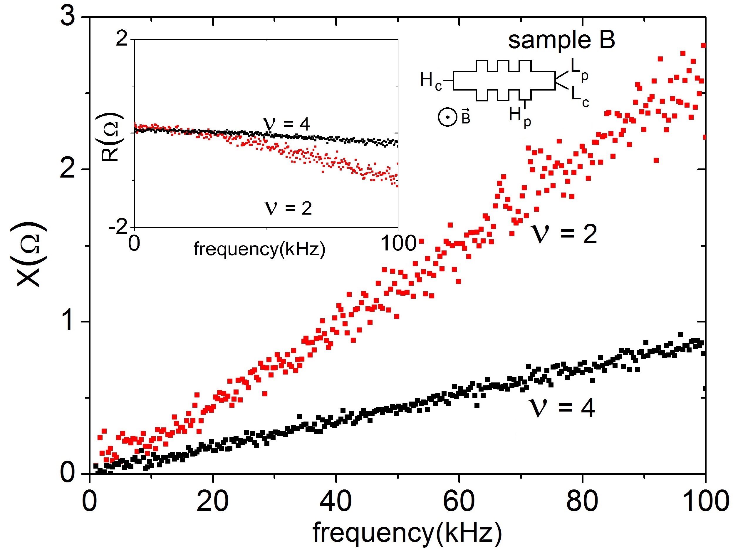
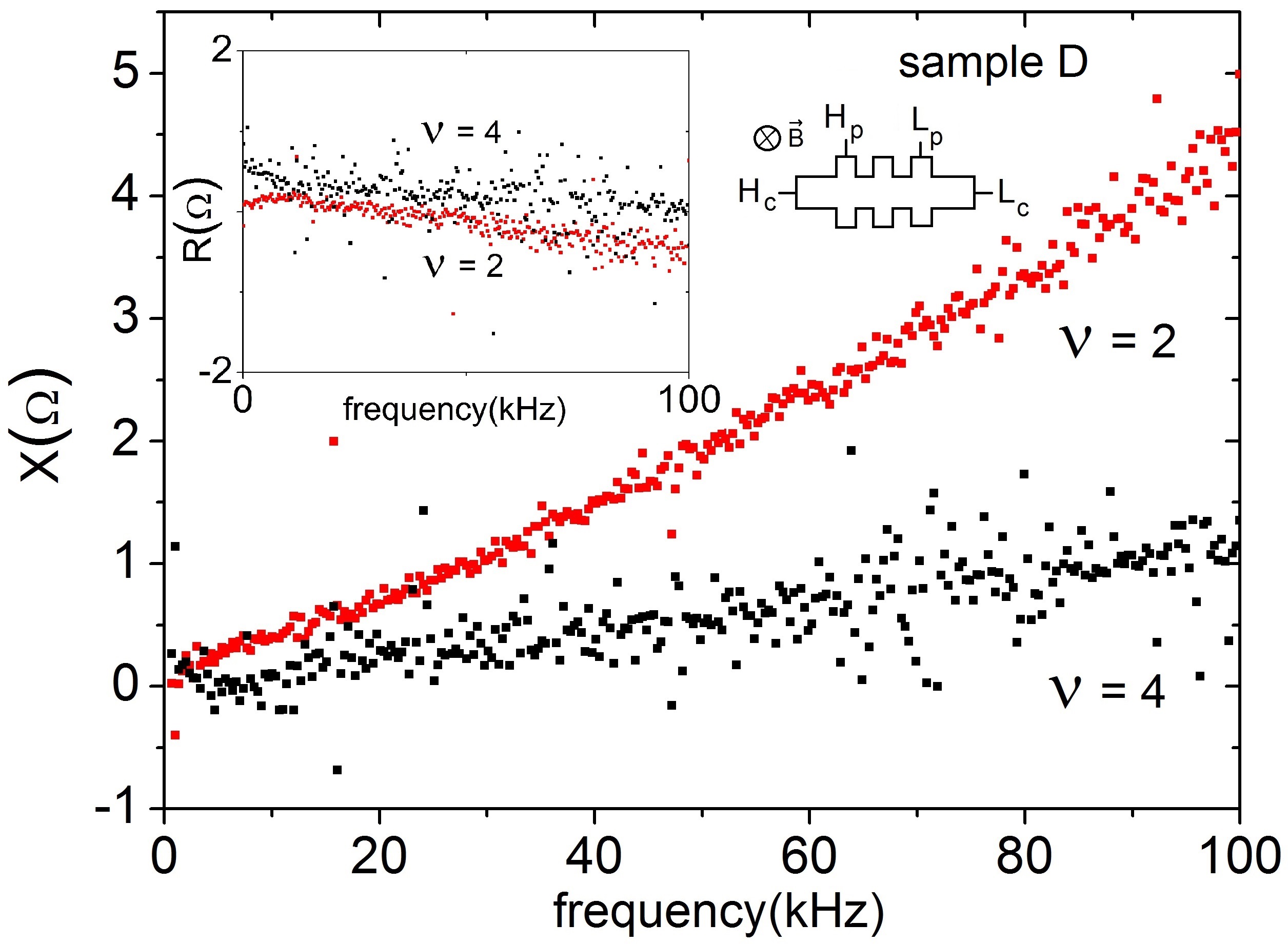
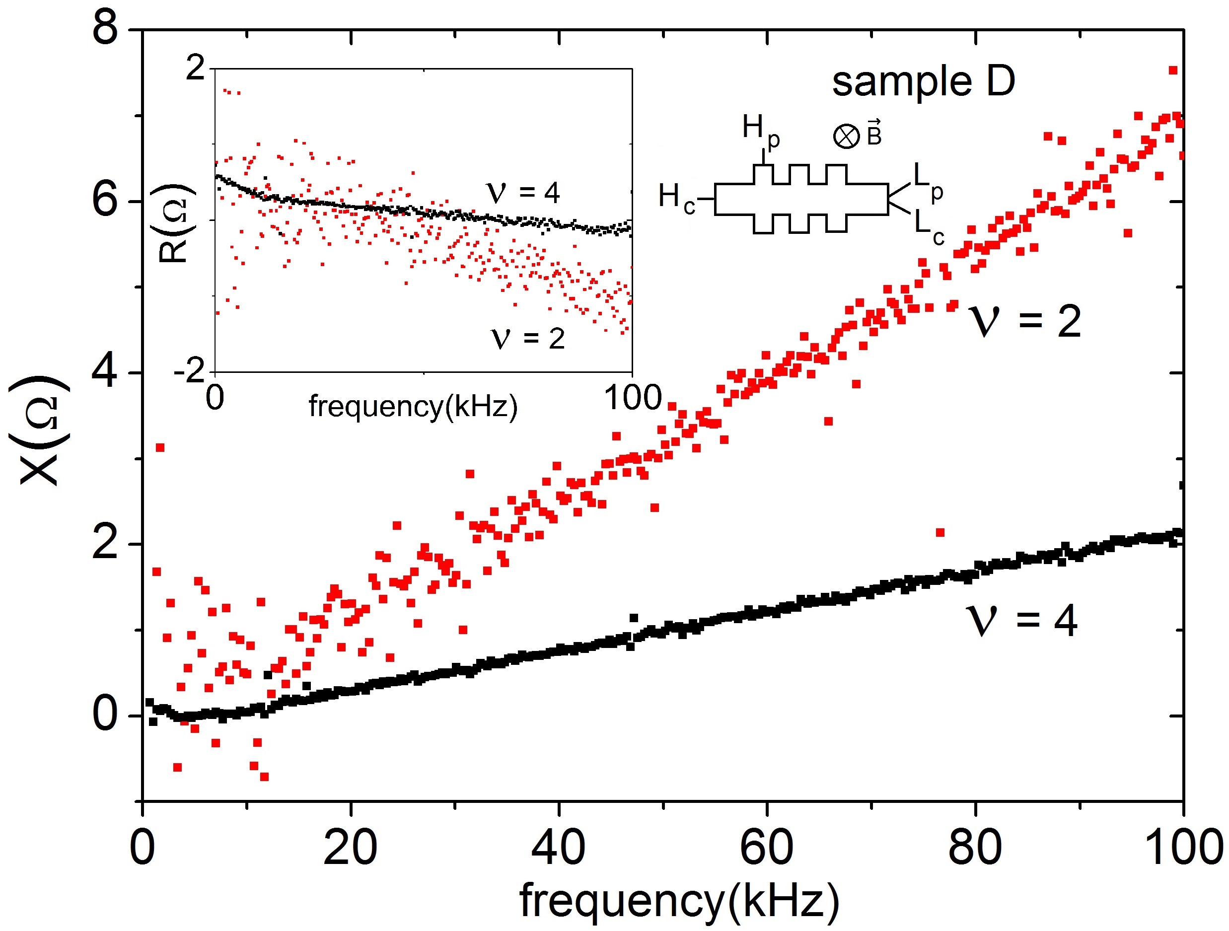
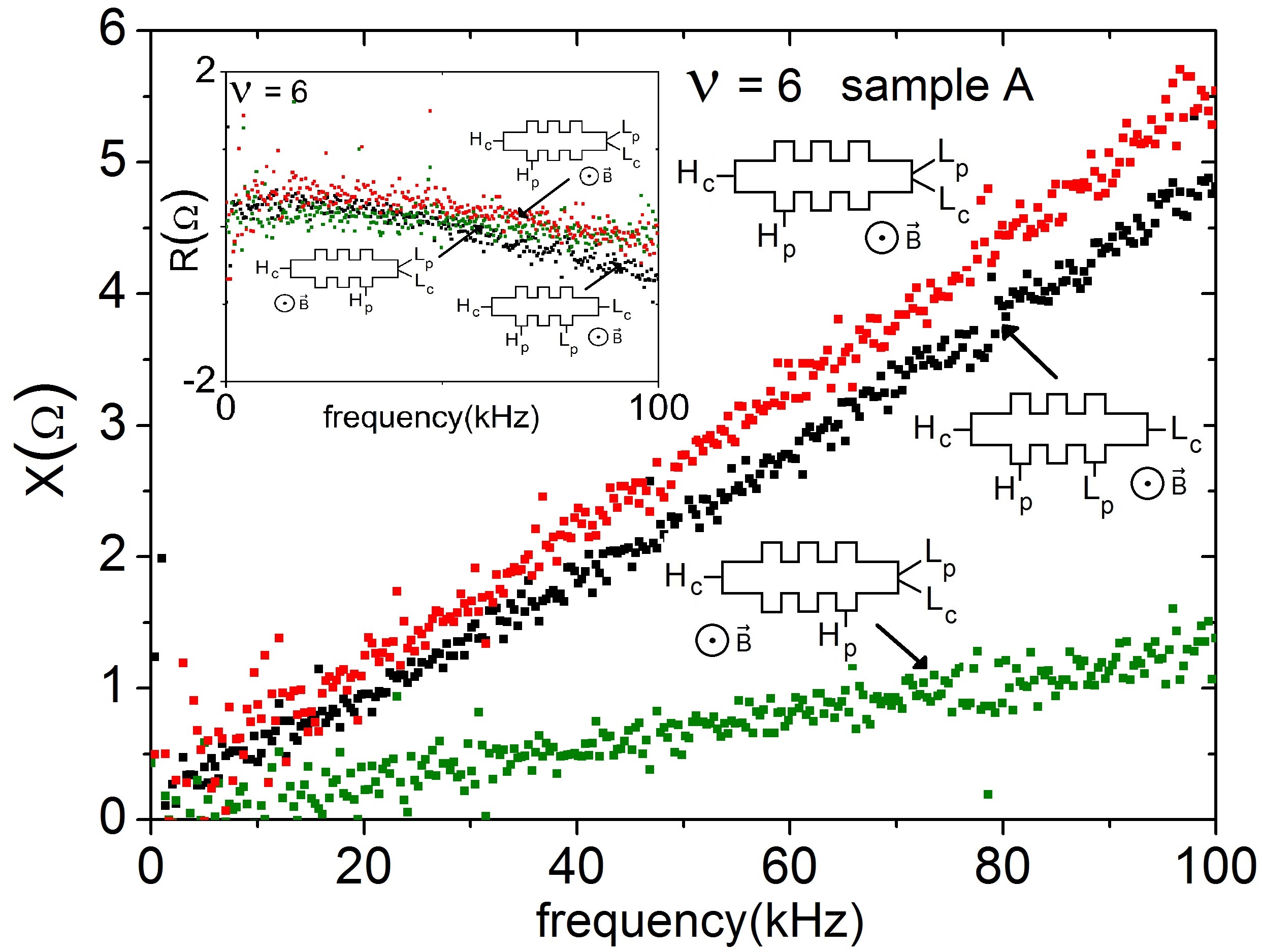
Figure 2 presents unfiltered and non-averaged raw data for the reactance in a given sample configuration for , , and . The positive linear dependence of is the signature of an inductive behavior. The corresponding inductance decreases with . These data are completely reproducible in the regions of magnetic fields where . This is a key point of our work: for integer filling factors, the real part of the measured impedance is close to zero with values between at low frequency as shown in the inset of Fig. 2. These results extend the work of Gabelli et al Gabelli et al. (2007) in which the sample resistance was , to the case of a zero resistance macroscopic device. At higher frequencies, a small real part of the measured response function appears. This effect is discussed in Appendix B and is correlated to the deviation of the reactance from linearity seen on Fig. 2.
Since the ac transport properties of a quantum Hall conductor is directly realted to the scattering of edge-magnetoplasmons Safi and Schulz (1995); Safi (1999); Bocquillon et al. (2013), we have developed an analytical model (see Appendix C) in the spirit of Ref. Hashisaka et al. (2013) for scattering of EMP modes in a quantum Hall bar taking into account long range inter-channel Coulomb interactions. It assumes that, in our ungated quantum Hall bars, all edge channels of same chirality have the same velocity and are so strongly coupled that they see the same time dependent potential as in Ref. Song et al. (2018). Since edge states are distant from more than from shield of coaxial cables located beneath the sample holder, estimated parasitic capacitance to shield for edge states is below while the inter-edge capacitance is of the order of . Therefore, Coulomb interactions effects are dominated by the inter-edge capacitance . Finally, dissipation of EMP modes have been neglected, an hypothesis a posteriori satisfied in our samples.
In the geometry depicted on Fig. 1, the low frequency expansion of the measured reactance is of the form:
| (2) |
where denotes the total inductance for the quantum Hall bar delimited by a dashed red box on Fig. 1-b. Because here, the magnetic inductance is much smaller than the kinetic inductance (see Appendix A), can be obtained from the edge magnetoplasmon scattering model as
| (3a) | |||
| (3b) | |||
where is the length of the Hall bar (see Fig. 1-b), is the quantum capacitance of edge channels and the geometric capacitance describes the effect of Coulomb interactions between counter-propagating edge channels. This is different from the quantum RL-circuit where, because of the gating, the capacitance has to be replaced by the capacitance with the nearby gates leading to a renormalization of by for right and left moving charge density waves Gabelli et al. (2007). Here, the renormalization factor involves a capacitance with the series addition of the quantum capacitances of counter-propagating edges. As a consequence, Eq. (3) still relates to the Hall resistance and to the electrochemical capacitance Christen and Büttiker (1996) defined as the series addition of to . Eq. (3) suggests that the inductance can be interpreted as a kinetic inductance associated with an effective time of flight . But, as discussed in Appendix C, is neither the drift velocity for non-interacting electrons nor even a renormalized electron’s velocity within chiral edge channels, but an effective velocity arising from the combination of their kinetic quantum inertia and Coulomb interactions within the quantum Hall bar. This effective inertia is of quantum origin, reflecting the minimal energy associated with an electrical current and appears, as we will see, to be dominated by the effects of Coulomb interactions.
The geometric capacitance depends on the width of the sample, and of the structure and geometry of the quantum Hall edge channels (see Appendix D), through a length proportional to the width of a single channel. Following Ref. Chklovskii et al. (1992), , which is of the order of a few tens of for AlGaAs/GaAs quantum Hall systems. Finally, the inter-edge Coulomb interactions contribution to
| (4) |
is found to be linear in , because of its proportionality to the quantum Hall conductivity , but with a logarithmic multiplicative correction which is a signature of Coulomb interactions.
We will now discuss how this expression and the experimental data enable us to rule out some models for . We have considered two different models for the confining potential at the edge of the sample which leads to a different prediction for : in Ref. Mikhailov (2000), where is the cyclotron frequency and the Fermi wave-vector. This leads to a dependance whereas in Ref. Chaubet and Geniet (1998), the gradient of the potential is proportional to where is the magnetic length thereby leading to a scaling .
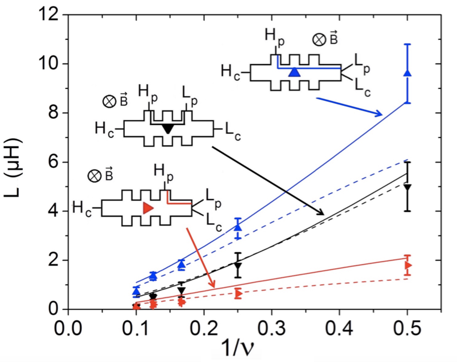
Fig. 3 contains the first main quantitative result of this work, i.e. the quantum inductance as function of for configurations ( configurations are analyzed in Appendix E). Values have been obtained from the reactance data depicted on Fig. 2 using the slope at low frequency of datasets. Three configurations in which and are plugged to different contacts (see Fig. 3) and thus correspond to different have been studied. The main result is the dependence of the inductance on which involves a linear part (see Eq. (3a)) due to the presence of channels in parallel, but with a non-linear correction stemming from the -dependence of (see Eqs. (3b)) together with Coulomb interaction effects (see Eq. (4)). The different dependences of lead to different theoretical predictions. We find that the scaling is the best for describing the experimental data.
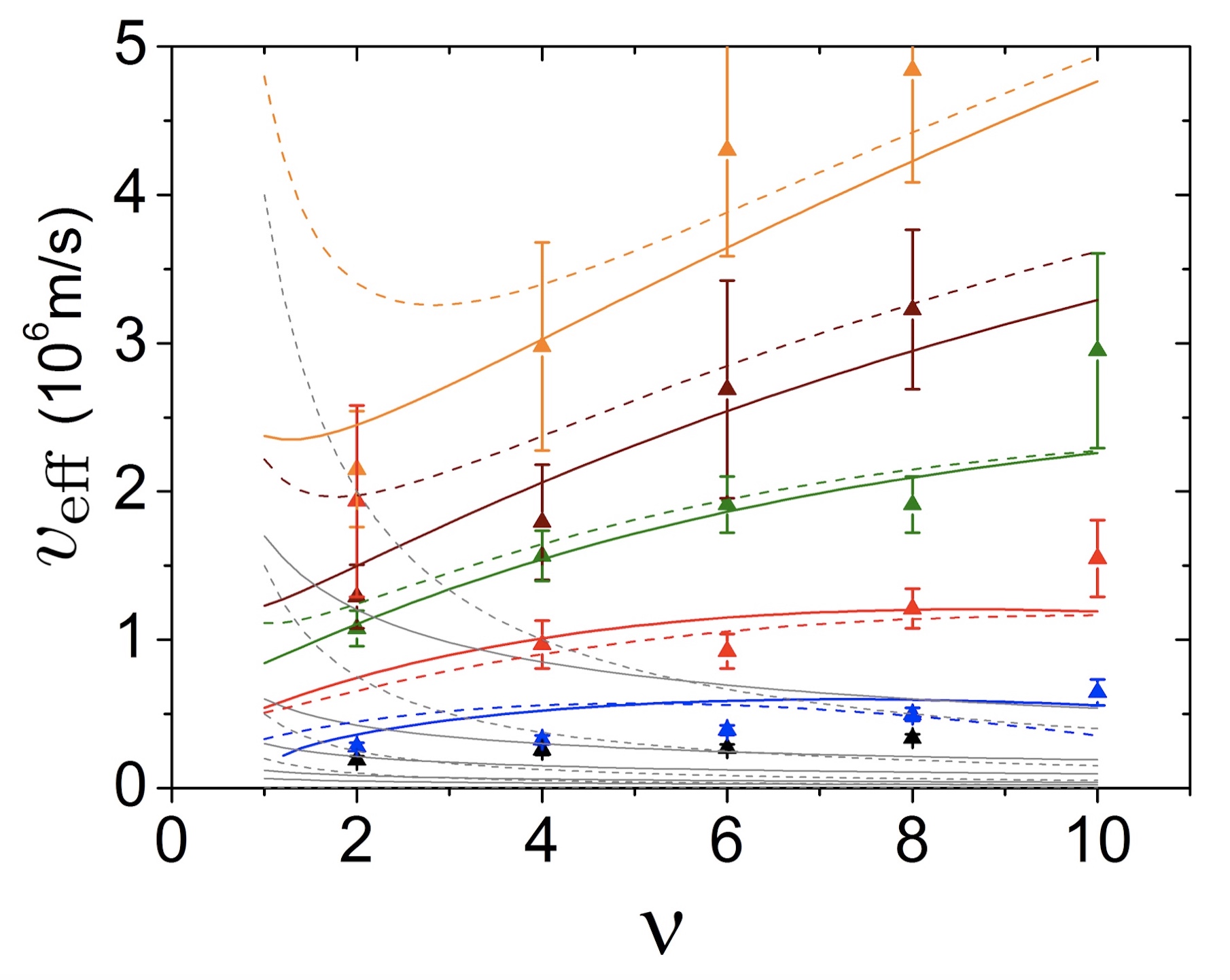
We have then extracted the velocity using Eq. (3a) from each value of the inductance (see Fig. 4). This is the second main quantitative experimental result of this work. Each family of points corresponds to a specific sample configuration for which the sample has been heated up, re-bonded and cooled down again. These manipulations affect the electrostatic arrangement of charges at the edge, thereby modifying from one experiment to the other. Fig. 4 presents predictions for from Eq. (1) for different models for . Simarily to the discussion of Fig. 3, the scaling for gives the best reproduction of the experimental data. But a striking point is that in order to reproduce the experimental data, it is necessary to take into account the inter-channel Coulomb interactions: ignoring the interactions would correspond to using instead of in Eq. (3a). This is shown by the thin filled and dashed grey curves on Fig. 4, which clearly do not follow the experimental data. We thus interpret the -dependence of when increasing from to (mostly linear with -correction) as a strong indication of the dominant role of Coulomb interactions in these ungated samples.
Let us comment on the spread of values for given in Fig. 4, which reflects the variability of the electrostatic environment in the samples from one experimental cooldown to another. A variation by a factor 25 is observed across all experiments (three higher curves for , all others for ) but by only a factor 6 when considering only one orientation of . This is still much larger than the relative change of the 2DEG density but reflects the edge potential, which may vary more from one experiment to the other. As we use a shallow etching technique, the samples edges are very sensitive to any change of the electric potential landscape222Additional results obtained on samples from different wafers are presented in Appendix E provide additional evidence of the robustness of our analysis.. The values that we have obtained for are compatible with estimates in the literature Roulleau et al. (2008) for shallow etched samples. Moreover, our measurements of are in the same range and qualitatively show a similar -dependence as the ones obtained in Ref. Kumada et al. (2011) for ungated samples by a time-of-flight technique.
To summarize, we have shown that, at low frequencies, a macroscopic quantum Hall bar is a perfect 1D conductor exhibiting a vanishing longitudinal resistance and a finite inductance. By fitting its dependence on and on the sample geometry using a simple long range effective Coulomb interaction model in the spirit of Büttiker et al Christen and Büttiker (1996), we have shown that it reflects the effective quantum inertia of charge carriers within the edges of the quantum Hall bar. Contrary to the case of superconductors where carrier inertia arises from the effective mass of the Cooper pairs, here it reflects how Coulomb interactions alter the propagation of low-frequency massless edge-magnetoplasmon modes. Remarkably, the experimental data can be understood using a simple model which is formally similar to the one used for gated nano-fabricated samples Hashisaka et al. (2012); Hashisaka and Fujisawa (2018): starting from chiral charge transport with bare velocity , we include Coulomb interactions with the other edges via classical electrostatics and edge structure geometry from Ref. Chklovskii et al. (1992). Going beyond this phenomenological but practical model would involve a multiscale treatment combining our approach to inter-channel interactions with a self-consistent microscopic approach solving the problem of electrons in the presence of intra-channel Coulomb interactions Armagnat et al. (2019); Armagnat and Waintal (2020); Roussely et al. (2018).
Finally, macroscopic samples may provide a rescaled test-bed for studying the scattering properties of edge-magnetoplasmons in to -sized samples. Studying a.c. transport properties of macroscopic samples up to radio-frequencies could thus open the way to realizing controlled quantum linear components for quantum nano-electronics in 1D edge channels, with possible applications to electron Bocquillon et al. (2014) and micro-wave quantum optics in ballistic quantum conductors Grimsmo et al. (2016).
Acknowledgements.
We warmly thank G. Fève, Ch. Flindt and B. Plaçais for useful discussions and suggestions as well as the referees for important comments and clarifications on this manuscript. This work has been partly supported by ANR grant “1shot reloaded” (ANR-14-CE32-0017) and the French Renatech network.Appendix A Kinetic and magnetic inductance
In this section, we compare the kinetic inductance of a quantum Hall bar at filling fraction to its geometric inductance.
A.1 Kinetic inductance
Let us first consider non-interacting chiral charge carriers with propagation velocity (see Fig. 5). As explained in the main text, for incompressible quantum Hall edge channels, this velocity is a drift velocity which depend on via the magnetic field and the dependence of the confining potential on itself as will be detailed in Sec. D.2. However, to keep notations simple, we shall denote it by instead of unless necessary.
A net current flow corresponds to a chemical potential between chiral edge channels of opposite chirality. The corresponding kinetic energy is then obtained by adding together the energy of all quantum states which have been occupied when biasing chiral edge states with different chemical potential :
| (5) |
where is the density of states (DOS) per unit length for a 1D-channel, the number of channels, the edge-state length. The voltage drop across the sample is , where denotes the quantum Hall resistance at filling fraction and the current. The resulting kinetic energy is then quadratic in the current, as expected for a linear inductor:
| (6) |
For a quantum Hall bar, we have two counter-propagating groups of chiral edge channels. Assuming that the two chiralities carry equal charge of the total current , this leads to a total kinetic energy
| (7) |
Using , we obtain the following formula for the inductance of the quantum Hall bar:
| (8) |
Note the appearance of the half of the time of flight of the electrons across the quantum Hall bar which is ultimately due to the existence of two counter-propagating groups of copropagating edge channels.
A.2 Magnetic inductance
A quantum Hall bar can be viewed as a conductor built from two linear wires of length , and of diameter or width separated by a distance which is the width of the quantum Hall bar. The magnetic inductance of the resulting dipole can be computed from Biot-Savart’s law Rosa (1908). Note that the wire’s diameter usually scales as (see Ref. Chklovskii et al. (1992) and Sec. D.1). In the quantum Hall bar geometry, the total current flowing across the quantum Hall bar corresponds to along each of the two long counter-propagating edges. Consequently, in the limit , the geometric inductance of the quantum Hall bar is approximately equal to
| (9) |
where is the magnetic permeability of the material expressed as the product of its relative permeability by the vacuum permittivity . For a non-magnetic material such as AlGaAs/GaAs, and therefore .
Using this expression and Eq. (8), the ratio of the magnetic to the kinetic inductance is given by:
| (10) |
where is the fine structure constant. The magnetic character of this ratio appears through the multiplication factor . Together with the smallness of and the logarithmic dependence in the aspect ratio , this explains why the magnetic inductance is always much smaller than the kinetic one for .
Appendix B Experimental signals
In this section, we discuss how the quantities that are measured in the experiment are related to the a.c. response of a quantum Hall bar even in the presence of experimental imperfections such as cable capacitances.
B.1 Finite frequency transport in quantum Hall edge channels
In his pioneering work on finite frequency charge transport in mesoscopic conductors Büttiker et al. (1993), Büttiker stressed the importance of interactions: time dependent drives applied to reservoirs lead to charge pumping in the conductor which, in return, alter the electrical potential within the conductor. As a result, its transport properties can no longer be derived by using the d.c. response at zero bias. Büttiker then developed a self consistent mean-field approach to this problem, taking into account how the time dependent charge density within the conductor generates a time-dependent potential and thereby alters the transport Prêtre et al. (1996). In the linear regime, the a.c. response of the conductor is described by the admittance matrix
| (11) |
giving the average current entering the conductor from lead when a voltage drive at the same frequency is applied to the reservoir . Charge conservation and gauge invariance imply that the finite frequency admittance matrix satisfy the general sum rules
| (12a) | ||||
| (12b) | ||||
which is ensured by total screening of effective Coulomb interactions.
At low frequency, this admittance matrix is expanded in , the zero-th order term being its d.c. conductance . The first order term is related to the emittances introduced by Büttiker et al. :
| (13) |
For quantum Hall edge channels, Christen and Bűttiker Christen and Büttiker (1996) fully exploited the chirality of charge transport to compute the dc conductances as well as the emittances using a discrete element description of the circuit.
Here we will show how to describe the finite frequency transport using the building blocks of a discrete element description of quantum Hall bars and the finite frequency admittance properties obtained from the edge-magnetoplasmon (EMP) scattering approach. The details of how the admittances are obtained from the EMP scattering approach are described in Sec. C.
Depending on the sign of the diagonal emittances, the quantum conductor under consideration exhibits a capacitive () or inductive () behavior. Basic examples of these behaviors, involving two different two-contact devices, have been given by Christen and Bűttiker Christen and Büttiker (1996). A two-contact Hall bar is predicted to act as an inductance while a ring shaped sample (the so-called Corbino geometry) acts as a capacitance. Hence both geometries exhibit opposite diagonal emittances, which can be understood in terms of reaction of the circuit to an injected charge. Indeed, as shown on Fig. 1 of Christen and Büttiker (1996) a charge injected by contact 1 into a Hall bar is transmitted to contact 2, while the charge induced by inter-edge Coulomb interactions created at contact 2 is transmitted to contact 1. On the contrary, in a Corbino sample, the injected charge returns to the contact it comes from, as does the image charge. It was experimentally shown by Delgard et al. Delgard et al. (2019) that Corbino emittances will exhibit this predicted capacitive behavior. Here, we will highlight the inductive behavior of quantum Hall bars in a multi-contact geometry that ensures vanishing longitudinal resistance.
We shall now discuss how, for two different sample configurations, the measured response function relates to the finite frequency admittance of the quantum Hall bar depicted as a red dashed rectangle in the two forthcoming figures, taking into account capacitive leaks at the contacts.
B.2 Three contact geometry
Let us first consider the three contact geometry depicted on Fig. 6. Contacts and are directly connected to reservoirs whereas contact is not but we take into account the cable capacitance of the cable. In this section, we shall compute the experimentally measured finite frequency impedance
| (14) |
up to second order in and show how it relates to the properties of the quantum Hall bar and to the cable capacitance (see Fig. 6).
B.2.1 Obtaining
In this approach, the quantum Hall bars and delimited on Fig. 6 are characterized by their frequency-dependent EMP scattering matrix. For the quantum Hall bar , the EMP scattering matrix, which we denote here by relates the ingoing and outgoing currents through Slobodeniuk et al. (2013)
| (15) |
in which the edges of the Hall bar are labeled by their chirality. In the same way, the EMP scattering matrix of the quantum Hall bar will be denoted by . These matrices are computed in Sec. C but for the moment, we won’t need their explicit form.
At contact , the incoming and outgoing currents propagating within the edge channels are also related by an input/output relation that reflects the time delay associated with the relaxation time of the contact:
| (16) |
Eliminating the edge channel currents internal to the sample directly leads to the finite frequency admittances connecting the currents entering from the reservoirs to the drive voltage :
| (17) |
in which the matrix elements of the Hall bar’s current scattering matrices and are involved as well as , the edge current transmission of the Ohmic contact with cable capacitance . For simplicity, the dependence of , and of the scattering matrix elements of the and quantum Hall bars as well as of have been omitted. The potential of the contact can also be computed as
| (18) |
which finally leads to
| (19) |
Note that, at low frequency (), the result only depends on the finite frequency properties of the quantum Hall bar i.e. the dipole under test in this setting.
B.2.2 Effect of the finite frequency deviation of from on
It is then useful to relate to the impedance of the Hall bar , which we know has a real part , with a small deviation for , as observed by metrologists studying the quantum Hall resistance a low frequencies [15-17].
This is achieved using the relation Safi (1999); Degiovanni et al. (2010) between the quantum Hall bar finite admittance matrix and its edge-magnetoplasmon scattering matrix to obtain the following expression, valid when the left and right moving edges of the quantum Hall bar are in total mutual influence:
| (20) |
in which denotes the dimensionless impedance of the quantum Hall bar in units of . Note that within the framework of the edge-magnetoplasmon scattering model presented in Sec. C, where is given in terms of the edge-magnetoplasmon scattering matrix by Eq. (52b). It thus predicts predicts and therefoe .
However, we will now show that a non vanishing is responsible for the non-linearity of seen on Fig. 2 of the paper. Such a feature has been observed for long time by metrologists studying quantum Hall resistance at low frequencies Chua et al. (1999); Schurr et al. (2005); Jeckelmann and Jeanneret (2001). In the metrology community, this finite frequency deviation from the dc quantum Hall value is commonly attributed to parasitic effects such as self and resistance of ohmic contacts and bond wires and thus depend on configurations and samples. A quadratic dependence on the frequency is usually found in the form . The parameter has been measured in many configurations and samples and has been found to be positive or negative but is always around (or below) Chua et al. (1999); Jeckelmann and Jeanneret (2001); Schurr et al. (2005).
To discuss the experimental results, which include both the real and imaginary parts of , let us therefore write
| (21) |
in which denotes the frequency-dependent deviation to (when non zero), and is the dimensionless frequency-dependent effective -time of the quantum Hall bar (). The low frequency expansion of the experimentally measured impedance is then
| (22a) | ||||
| (22b) | ||||
In our experiments, the reactance is obviously dominated by the kinetic inductance :
| (23) |
but is seen through the deviations of the imaginary part from linearity (see Fig. 2 of the paper). It is nevertheless small and therefore, the dominant contribution to the real part is a negative quadratic one directly proportional to the cable capacitance: , as observed in the inset of Fig. 2 of the paper.
Both real and imaginary part of admittance seen in Fig. 2 suggest a quadratic behavior for . To second order in :
| (24) |
where .
In our experiments, the cable capacitance is . We deduce from Fig. 2 of the paper that, at and , . This gives at thereby corresponding to , a value in total agreement with the deviations reported in the litterature. Consequently, the observed deviations from pure inductive behavior can be explained by the combined effect of the cable capacitance and of the deviations of from its dc value .
B.3 Four contact geometry (two on the same side)
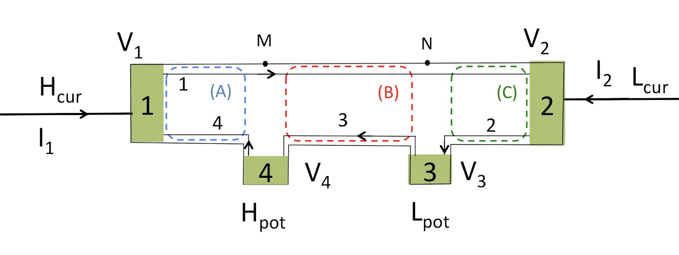
Let us now turn to the case of a four contact sample depicted on Fig. 7. This geometry represent a four contact measurement of the central part of the device. Here, the parts and of the device play the role of the leads that connect to the current injection reservoirs which are the Ohmic contacts and . The Ohmic contacts and are used for measuring the voltage difference between the two port of the would-be dipole .
In this section, the capacitances of the cables will be omitted for simplicity. This does not change the physics of the problem but greatly simplifies the computations. Nonetheless, we know from Eq. (16) that the same prefactor will appear in the results when capacitances are taken into account.
We assume that , and can be modeled as quantum Hall bars characterized by their edge-magnetoplasmon scattering matrices. Exactly as before, this amounts to neglecting Coulomb interactions outside the Hall bars themselves, an hypothesis consistent with the total screening hypothesis stated in Sec. C.1. Let us denote by and the points on edge channel 1, which respectively face contacts 4 and 3. Introducing the EMP scattering matrices , and respectively associated with the three quantum Hall bars , and represented on Fig. 7, the dynamics of the three quantum Hall bars is described by:
| (25a) | ||||
| (25b) | ||||
| (25c) | ||||
in which, for compactness, the dependence is not recalled. In the experimental configuration depicted in Fig. 7, and we measure . We calculate and , in order to find . The lead potentials fix the incoming currents injected by the reservoirs. Moreover, because of the high impedance of the voltmeter connected to and , we neglect the currents leaking into these Ohmic contacts. We thus have:
| (26a) | ||||
| (26b) | ||||
| (26c) | ||||
| (26d) | ||||
From Eqs. (25a) and (25b), we obtain :
| (27) |
or, equivalently:
| (28) |
On the other hand, calculating :
| (29) |
using now Eq. (25c), this becomes a current division relation where
| (30) |
Eqs. (25a) to (25b) then shows that . We now use Eq. (25a) to express in terms of and . Using Eq. (28), we obtain :
| (31) |
This gives us the total current entering lead in terms of the applied voltage at the right Ohmic contact:
| (32) |
Using one last time the voltage division relation (28), the dimensionless impedance is thus finally given by:
| (33) |
As in the three contact case, the fraction appears in the results showing that the four point measurement does gives us information on the quantum Hall bar. However, the matrix is involved via the quantity . Nevertheless, it is possible to show that, to the lowest order frequency expansion, does not depend on the physical relevant information contained within the C matrix. For this we once again use the low frequency expansion of the scattering matrix (see Eq. (49)):
| (34) | ||||
| (35) |
where is the length of Hall bar , and is the transit time across the Hall bar . These formulas allow the calculation of quantity from its definition by Eq. (30) at the first order in :
| (36) |
Finally, using Eq. (33),
| (37) |
showing that the measured inductance corresponds to the transit time in Hall bar . Thus, the length involved in the determination of velocities is .
Appendix C Discrete element description from edge-magnetoplasmon scattering
In this Section, we present the computation of the EMP scattering matrix for an ungated quantum Hall bar and derive the corresponding description in terms of discrete elements valid at low frequency.
C.1 The model
We consider a quantum Hall bar of length in the integer quantum Hall regime with filling fraction as depicted on Fig. 8. We denote by (resp. ) the upper (resp. lower) edge channels which are right (resp. left) movers as depicted on Fig. 8. We denote by the incoming current entering the Hall bar on side , and the outgoing one. Our goal is to relate the outgoing currents to the incoming ones in the presence of Coulomb interactions.
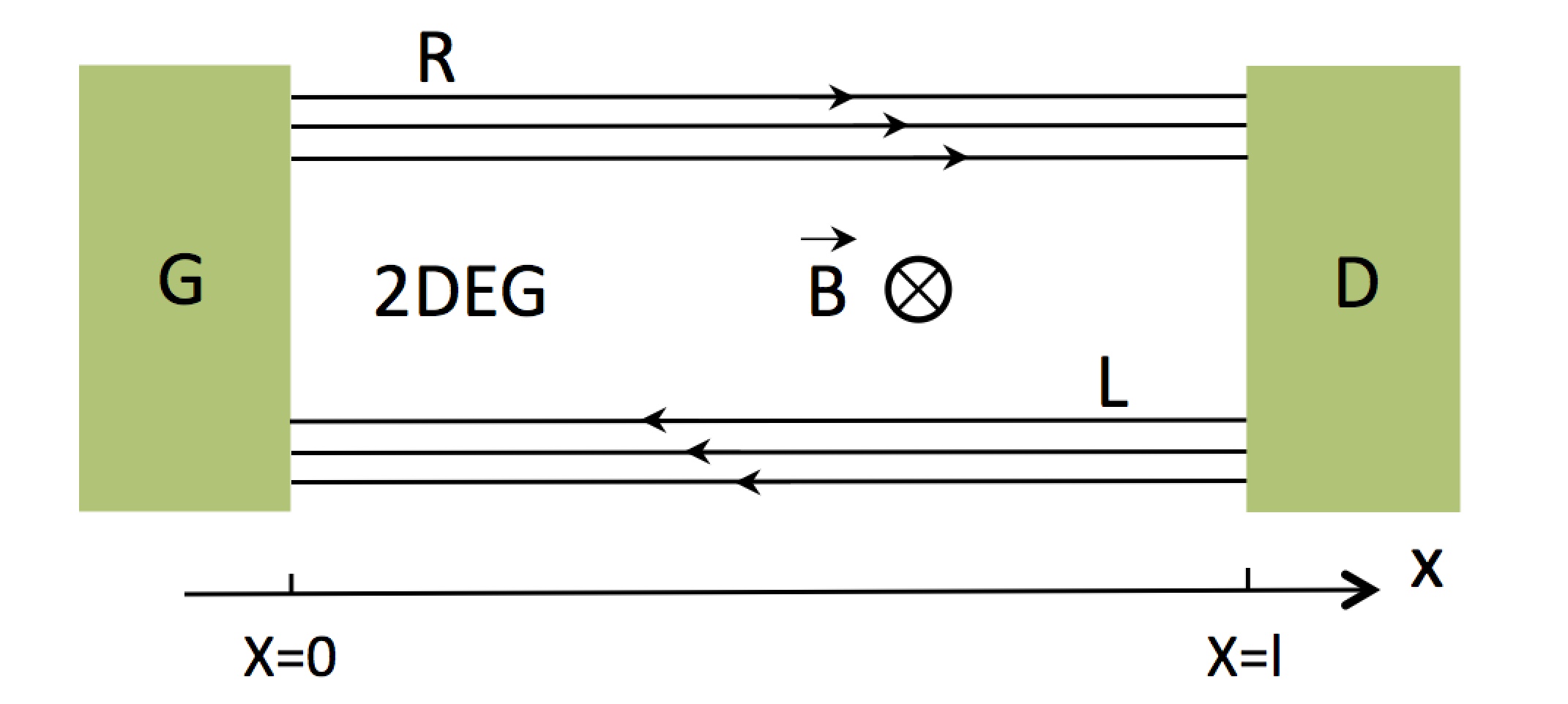
Here denotes the charge transport velocity, which for simplicity we take identical for all chiral edge channels. Coulomb interactions are described by assuming a discrete element model à la Christen-Büttiker Christen and Büttiker (1996) in which all the electrons within channels of the same chirality see the same time dependent potential (for right movers) and (for left movers). These potentials are related to the total charge stored within the and edge channels by a capacitance matrix
| (38) |
in which
| (39) |
and denotes the capacitance matrix
| (40) |
where depending on the screening of Coulomb interaction between channels of opposite chiralities by nearby gates and other on-chip conductors. Eq. (38) plays the role of a solution of the Poisson equation relating the electrical potential to the charge density. In this work, unless otherwise stated, we assume that the left and right chiral edge channels are in total influence and therefore that . The capacitance can then be computed as the geometric capacitance of a stripline capacitor (see Sec. D).
The charges within the edge channels are directly related to the incoming and outgoing currents through charge conservation which, in the Fourier domain and in vector notation, is written as
| (41) |
The last equation we need is the equation of motion for the charge or current density within the Hall bar Cabart et al. (2018):
| (42) |
in which , and
| (43) |
represents the effective quantum capacitance at frequency for the edge channels of length and filling fraction . Eq. (42) expresses that the charge stored within each edge channels comes from what is injected by the reservoirs and from the shift of the bottom of the electronic bands by the electric potential seen by all electrons.
C.2 Edge magnetoplasmon scattering
Using Eqs. (38) and (41) to eliminate and from Eq. (42) leads to
| (44) |
Solving this equation leads to the scattering matrix relating incoming to outgoing electrical currents at . From the bosonization point of view, this is the scattering matrix for the bosonic counter-propagating edge-magnetoplasmon modes carrying the total charges of the right and left moving edge channels.
This scattering matrix depends on a dimensionless coupling constant characterizing the strength of Coulomb interactions within each edge channel by the way of the ratio of the bare quantum capacitance of a single edge channel with drift velocity to the geometric capacitance 333The dependence of is restored here to stress that we are in the limit of a long quantum Hall bar () where it is linear in .:
| (45) |
The higher this number, the higher is Coulomb’s energy with respect to the kinetic energy scale . The geometric capacitance can be evaluated using standard electrostatics as explained in Sec. D. The result comes under the form
| (46) |
in which is the relative permittivity of the material and is a geometrical factor that depends on the width of the quantum Hall bar and on , the width of the system of copropagating edge channels at the edge of the quantum Hall bar. The latter is proportional to the filling fraction and, in the limit, the geometric factor depends logarithmically on the aspect ratio as shown in Sec. D. The dimensionless coupling constant
| (47) |
is therefore proportional to the effective fine structure constant at filling fraction
| (48) |
up to a subdominant logarithmic dependence in arising from classical electrostatics (see Sec. D). The dependence is an dependence involving the free electron time of flight along the edges of the quantum Hall bar. Solving Eq. (44) leads to the edge magnetoplasmon scattering amplitudes
| (49a) | ||||
| (49b) | ||||
Note that the relation between diagonal and off diagonal matrix elements given by Eq. (49b) is only valid for total screening (). One should also note that because of the symmetric setup considered here, the edge magnetoplasmon scattering matrix is determined by its diagonal coefficient and its off-diagonal coefficient . They satisfy the unitarity conditions
| (50a) | ||||
| (50b) | ||||
which ensure energy conservation within the quantum Hall bar.
C.3 Finite frequency impedances
In the spirit of Büttiker, let us derive a discrete element circuit description of the quantum Hall bar. In full generality, this description involves a three terminal circuit in order to take into account the electrostatic coupling to external gates which are assumed to be at the ground here (see Fig. 9). In our experimental, ungated samples, this coupling is expected to be small as we shall see. Note that the symmetry of the Hall bar under magnetic field reversal justifies considering two identical impedances on both sides of the central node on Fig. 9. For this tri-terminal circuit, one can combine the relation between the potentials , , and (by gauge invariance) and the current sum rule to relate and to and :
| (51) |
On the other hand, the finite frequency admittance of the quantum Hall bar can be obtained from the edge magnetoplasmon scattering matrix which, in the present case is symmetric. We can then infer expressions for the impedances and in terms of the EMP scattering matrix of the quantum Hall bar:
| (52a) | ||||
| (52b) | ||||
Note that Eqs. (52a) and (52b) have been obtained without any explicit assumption of total screening. In the case of (total screening, see Eq. (40)), is expected to be infinite and is indeed found to be infinite since, in this case, (see Eq. (49b)).
To obtain the simplest effective circuit description, we just derive the dominant terms of the low frequency expansion of and by expanding the edge-magnetoplasmon scattering matrix in powers of . This leads to (total screening) and
| (53) |
which shows that the impedance can be viewed as the series addition of a resistance ( parallel single channel contact resistances ) and an inductance such that
| (54) |
The quantum Hall bar is then a dipole with impedance which then behaves as an inductance in series with the quantum Hall resistance at low frequency. Since is the total inductance of the quantum Hall bar, it follows that the electronic time of flight appearing in Eq. (8) is renormalized by Coulomb interactions. The corresponding renormalized velocity
| (55) |
can, in a sense, be interpreted as an effective charge velocity.
To understand this more precisely, let us imagine that the quantum Hall bar could be viewed as an ideal coaxial cable with channels with plasmonic velocity . This would lead to a diagonal plasmon scattering matrix: and . The corresponding admittance would then be given by
| (56) |
where the index tl emphasizes the transmission line description considered here. Its low frequency expansion would correspond to the series addition of the contact resistance with an inductance given by
| (57) |
Consequently, we also recover the analogue of Eq. (8) with playing the role of . However, in this transmission line model, the admittance would not vanish, thereby showing that such a transmission line model cannot describe the totally screened situation. The edge magnetoplasmon scattering matrix derived in Sec. C.2 shows that, in the totally screened case, vanishes.
Appendix D Geometric capacitance
In this section, we compute the geometric capacitance of the quantum Hall bar using as model a capacitor built from two coplanar strips corresponding to the two counter-propagating edge channel systems.
D.1 Width of edge channels
The model of Ref. Chklovskii et al. (1992) by Schklovskii et al. describes the structure of quantum Hall edge channels when taking into account the effect of Coulomb interactions. It predicts the width (also denoted by following Ref. Chklovskii et al. (1992)) of the incompressible channels in term of the density gradient at the edge as well as the width of compressible channels as a function of .
The width of incompressible stripes is obtained by identifying the Landau gap with the energy variation of an electron in the confining potential (see Figure 10):
| (58) |
where denotes the gradient of within the incompressible part of the edge of the sample. As explained in the main text, the confining potential may depend on as discussed in Sec. D.2. For simplicity, we shall assume that this gradient has indeed the same dependence on as the charge transport velocity present in the equations of motion (42) and (43). This leads to:
| (59) |
where we have replaced the drift velocity within the incompressible stripe by the drift velocity along the edge by . Note that this expression is formally the Compton wavelength associated with a relativistic particle of mass and effective speed of light . This explains why we denote it by in the following. This result is not surprising, the width of the incompressible stripe is the minimal one for closing the cyclotron gap for an electronic excitation in the confinement potential, as shown in Ref. Chklovskii et al. (1992).
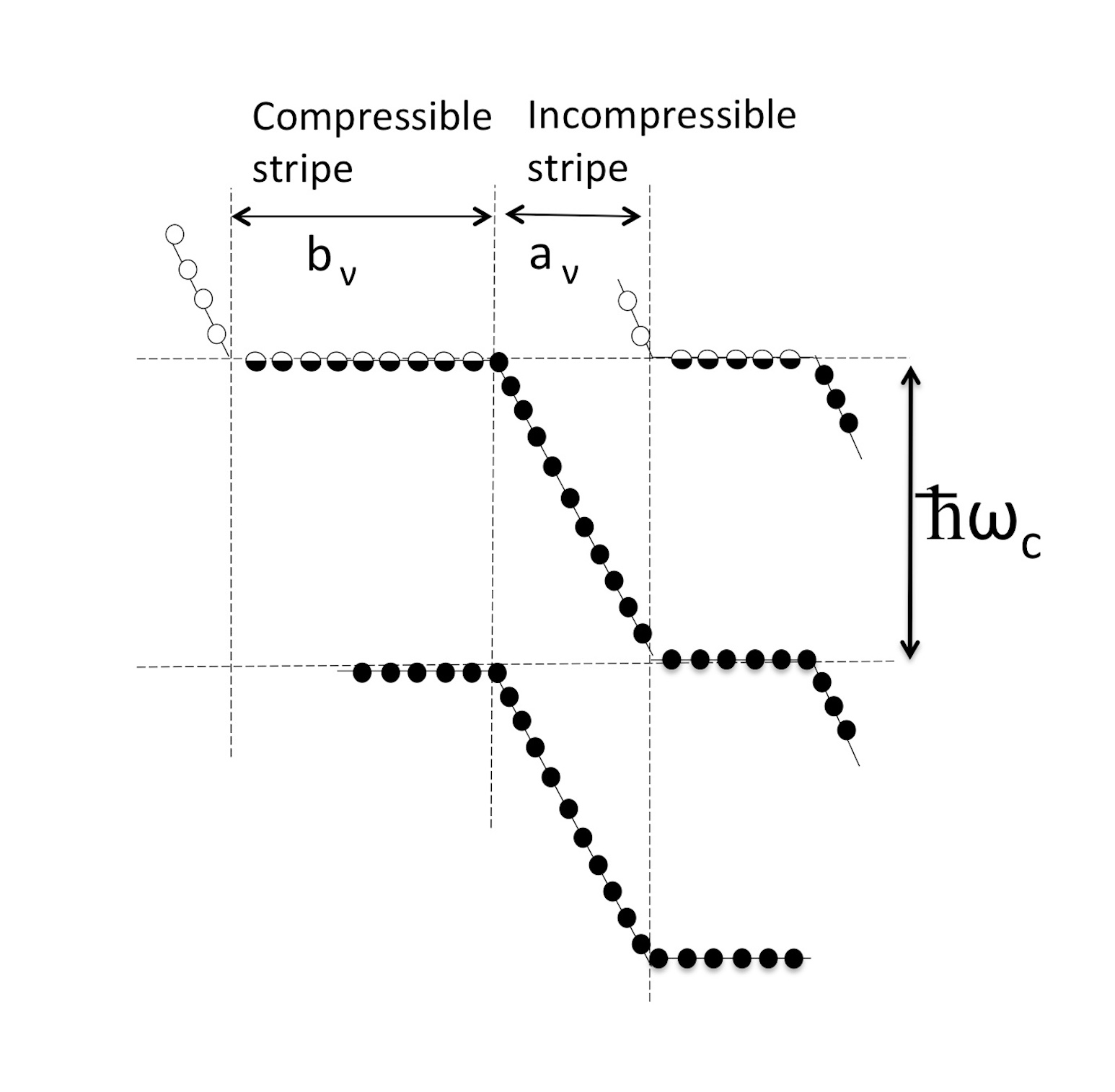
Once the width of an incompressible stripe is known, the width of a compressible stripe is given by
| (60) |
where denotes the effective Bohr radius in the material.
D.2 On the -dependence of
In this section, we discuss the -dependence of the confining potential . In the regime where no compressible stripes are present, this would be the chiral drift velocity associated with the confining potential at the edge of the sample . In the case of a smooth confining potential, compressible stripes may appear and the velocity refers to the effective charge velocity at the edge, arising from the dynamics of the compressible stripe coupled to the incompressible one Han and Thouless (1997). As explained before, our main hypothesis here is that this velocity can be used in the expressions (59) and (60) of the width of incompressible and compressible parts of the edge channels and that it has the same expression for all of them.
We discuss here two different forms for , one based on Ref. Mikhailov (2000) and the other one based on Ref. Chaubet and Geniet (1998):
| (61) |
Our discussion will be based on heuristic arguments which only identify with a drift velocity if the edge channel does not contain any compressible stripe Balev and Vasilopoulos (1998); Baleva et al. (2002). However, Han and Thouless have shown in Ref. Han and Thouless (1997) that, in the presence of the compressible stripe, the velocities of the eigenmodes propagating along the edge channel contain a contribution from the incompressible part drift velocity. We think that this justifies the heuristic arguments that will now be layed down.
In Ref. Mikhailov (2000), Mikhailov gave the following form for the edge velocity of plasmons due to the quantum confining potential: (Eq. 1-60). As the cyclotron frequency is inversely proportional to the filling factor , and only depends on the density of the 2DEG, this velocity is with for our sample.
We have used such velocity in Eq.(1) to fit the data. However, we have varied the numerical parameter around this value to fit our data in Fig. 4. As can be shown from Fig. 4 of the paper, the fitting values of are between and times the above estimation.
In Ref. Chaubet and Geniet (1998), which studies the breakdown of the IQHE, Chaubet and Geniet computed a confining potential by solving the problem of an harmonic oscillator with a boundary condition on the edge. They showed that, when the wave function equals zero at the edge, the eigen-energies are modified compared to the boundaryless problem and increase, giving a realist interpretation of the confining potential. In Fig. 9 of Ref. Chaubet and Geniet (1998), the confining potential – represented by the energy of states – increases nearly linearly with the distance from the edge. We thus approximate the gradient by the ratio of the cyclotron energy to the magnetic length: . The physical image is that the potential slope corresponds to an energy gain of the order of the Landau gap on a length scale . This gives a drift velocity which in the case of our sample leads to with .
Exactly as for the previous model, we have considered as a fit parameter that can be varied in order to represent all experimental situations in our experiments. As can be shown from Fig. 4 of the paper, the fitting values of are between and times the above estimation, a smaller range than with the model.
D.3 Capacitance computation
The quantum Hall edge channel system has a width
| (62) |
which is of the order of per edge channel in AlGaAs/GaAs systems. In the transverse direction, the electrons are confined within a triangular potential well. The typical extension of the electron’s wavefunction in the transverse direction is of the order of Fang and Howard (1966), therefore suggesting a rather flat shape of the edge channel.
A first estimate of the geometric capacitance of the edge channel system can thus be obtained by computing the geometric capacitance per unit of length of an infinite pair of coplanar strips of width separated by a distance Iossel et al. (1969):
| (63) |
in which denotes the elliptic integral of the first kind Gradshteyn and Ryzhik (1994) evaluated at where, in our case and is the total width of the quantum Hall bar. Using known asymptotics for the elliptic integral, we find the geometrical capacitance for the quantum Hall bar of width and length at filling fraction
| (64) |
On the other hand, using a more precise self-consistant solution of the electrical potential within quantum Hall edge channel arising from the repartition of quantum electrons, Hirai and Komiyama Hirai and Komiyama (1994) have shown that the capacitance can be obtained as the geometric capacitance of two parallel wires:
| (65) |
Expressions (64) and (65) are not identical, but both are considered in the regime where , that is, when they lead to similar estimates for the capacitance. Both expressions are of the form
| (66) |
where is a factor that depends on the specific model used to describe the charge repartition within the edge channels. Here in Harai et al.’s estimate and for the coplanar strip capacitance model. Using Eq. (66), the effective coupling constant is then
| (67) |
Using this expression into Eq. (55) leads to
| (68) |
for the ratio of to the drift velocity within a chiral edge channel. This expression can then be rewritten in terms of the effective single edge channel width :
| (69) |
Appendix E Supplementary results
In this Section, we show further experimental results obtained on sample A (the sample discussed in the paper) and on three other samples manufactured from three different AlGaAs/GaAs heterojunctions. Their wafer characteristics (electron density and mobility of the two-dimensional electron gas) are reported in table I. Samples have been processed on these heterojunctions using the same design and dimensions as for sample A. Exeperimental results obtained on these samples have been obtained using exactly the same protocols and they are completely similar to the results presented in the paper.
We first present complementary results on sample A, then we present results obtained on the other samples, which concern influence of filling factor and influence of edge channel length.
| Wafer | () | () | (for ) | Width () |
|---|---|---|---|---|
| A | 5.1 | 30 | 400 | |
| B | 3.3 | 50 | 1600 | |
| C | 4.5 | 55 | 400 | |
| D | 4.3 | 42 | 800 |
E.1 Complementary results on sample A
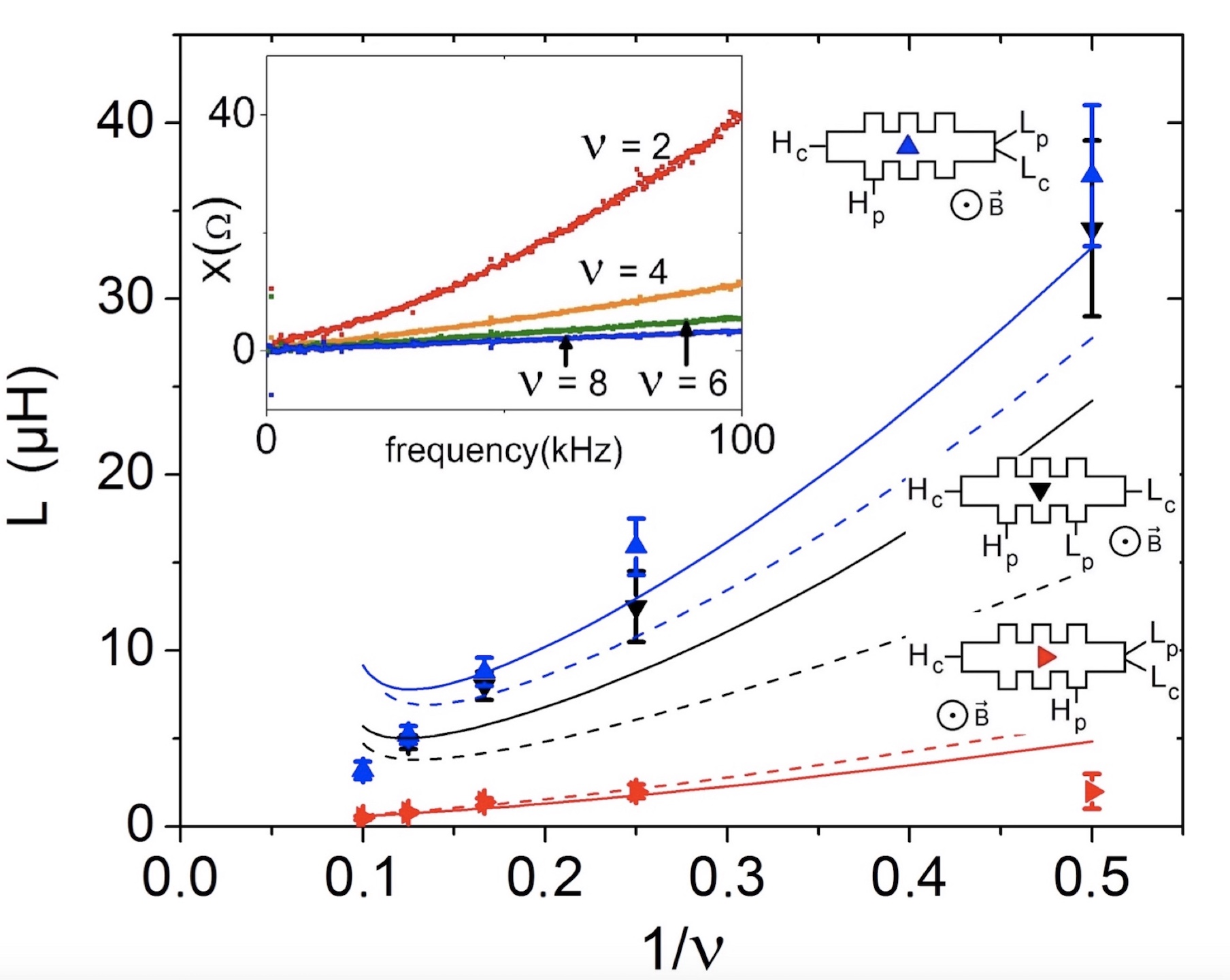
Fig. 3 of the paper shows, for a positive orientation of magnetic field, the dependence of the quantum inertia on the inverse of the filling factor. In Fig. 11, these results have been obtained for a positive orientation of magnetic field. Once again the models (dashed lines) and have been considered using a proper velocity for each configuration (see caption). Althougth the agreement between the experomental data and the theory is not as good as in the case of configurations, we still see that better reproduces the data (especially for the configuration.
E.2 Influence of filling factor for other samples
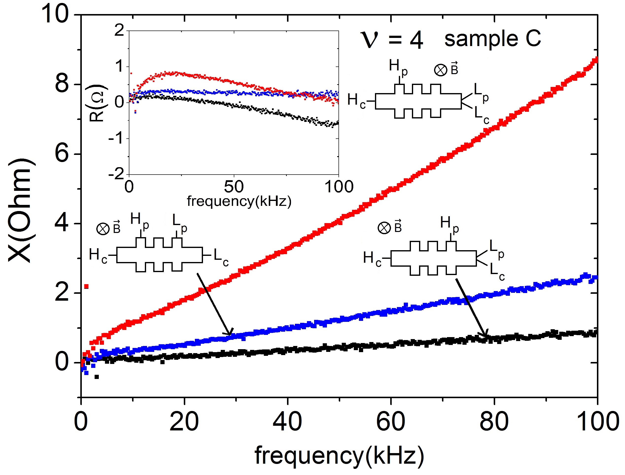
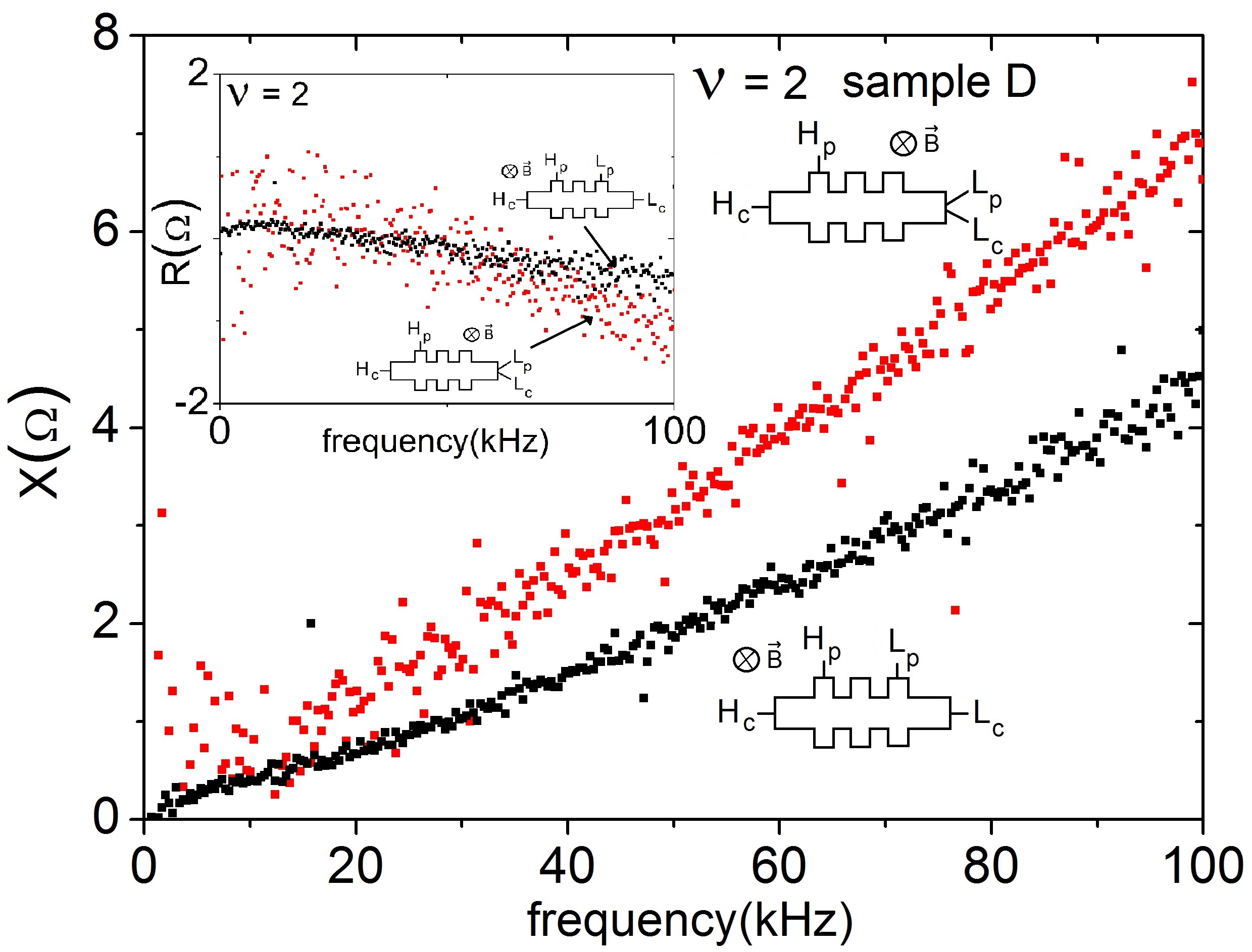
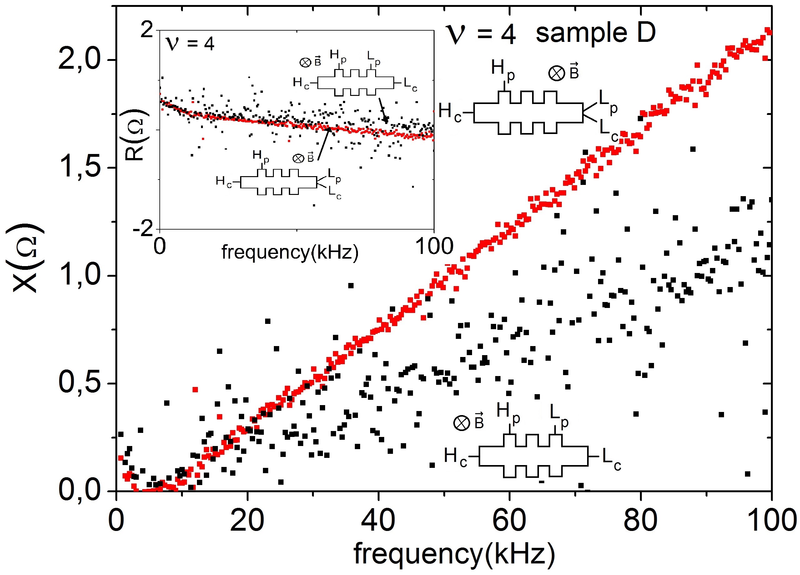
For sample A we have shown that reactance increases linearly with frequency and that the slope depends strongly on the filling factor. Here, we observe the same behavior on other samples (see Figs. 12 to 14): the slope decreases while the filling factor increases.
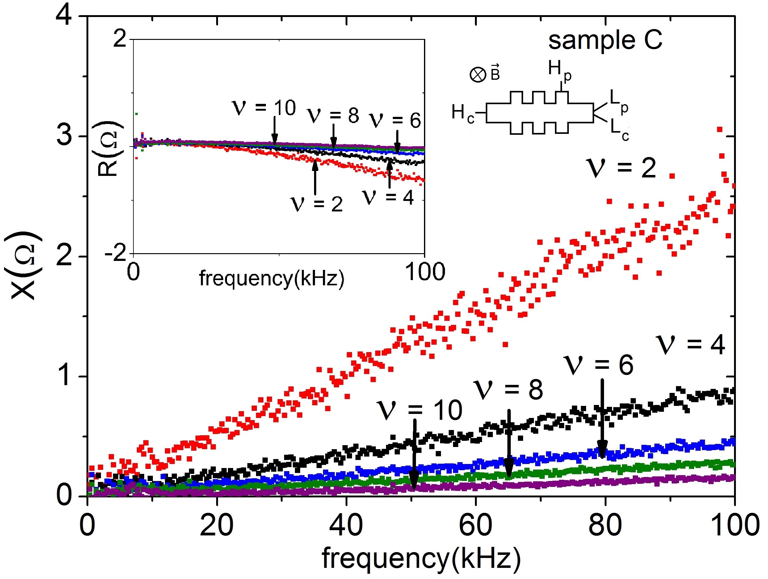
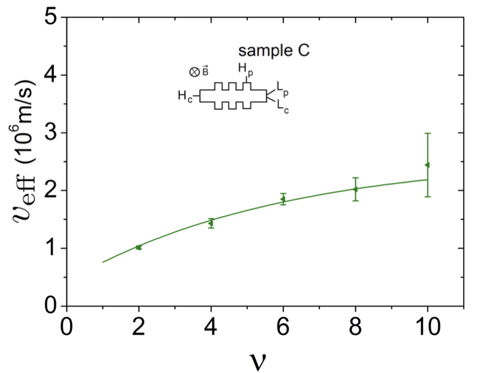
For Figs. 12, 13 and 14, the data have only been obtained for two values of . However, Fig. 15 displays all even values of from to for sample C in a given confuguration. It is then possible to try fitting these experimental data using Eq. (1) of the paper with . This fit is presented on Fig. 16 and show that our model also described correctly the experimental data for sample C with the configuration displayed on Fig. 15.
E.3 Influence of configurations for other samples
Figs. 17 to 20 depict the reactance as a function of frequency for three samples at different filling factors. For each sample at a given filling factor, we observe how the configuration (shown as an inset for each curve) modifies the slope of the reactance. Each configuration has its proper length and the larger the edge states the higher the quantum inertia. The length concerned here is the distance between potentials and .
Meanwhile, differences in velocity for distinct configurations imply that the ratio between quantum inertia and length of edge states not a constant. Configurations are obtained after wire-bonding the samples. This entails heating the samples and cool them down again afterwards, and this causes the velocity to change a bit from one configuration to another.
References
- Klitzing et al. (1980) K. v. Klitzing, G. Dorda, and M. Pepper, Phys. Rev. Lett. 45, 494 (1980).
- Halperin (1982) B. I. Halperin, Phys. Rev. B 25, 2185 (1982).
- Haug (1993) R. J. Haug, Semiconductor Science and Technology 8, 131 (1993).
- Weis and von Klitzing (2011) J. Weis and K. von Klitzing, Philosophical Transactions of the Royal Society A: Mathematical, Physical and Engineering Sciences 369, 3954 (2011), https://royalsocietypublishing.org/doi/pdf/10.1098/rsta.2011.0198 .
- Suddards et al. (2012) M. E. Suddards, A. Baumgartner, M. Henini, and C. J. Mellor, New Journal of Physics 14, 083015 (2012).
- des Poids et Mesures (1988) C. I. des Poids et Mesures, “Représentation de l’ohm à partir de l’effet hall quantique,” Recom. 2 (CI-1988) 77th Session (1988).
- Jeckelmann and Jeanneret (2001) B. Jeckelmann and B. Jeanneret, Reports on Progress in Physics 64, 1603 (2001).
- Ahlers et al. (2009) F. J. Ahlers, B. Jeanneret, F. Overney, J. Schurr, and B. M. Wood, Metrologia 46, R1 (2009).
- Delahaye (1995) F. Delahaye, Metrologia 31, 367 (1995).
- Chua et al. (1999) S. W. Chua, A. Hartland, and B. Kibble, IEEE Transactions on Instrumentation and Measurement 48, 309 (1999).
- Schurr et al. (2005) J. Schurr, B. Wood, and F. Overney, IEEE Transactions on Instrumentation and Measurement 54, 512 (2005).
- Cage and Jeffrey (1996) M. E. Cage and A. Jeffrey, J. Res. Natl. Inst. Stand. Technol. 101, 733 (1996).
- Jeanneret et al. (1995) B. Jeanneret, B. D. Hall, H.-J. Bühlmann, R. Houdré, M. Ilegems, B. Jeckelmann, and U. Feller, Phys. Rev. B 51, 9752 (1995).
- Schurr et al. (2011) J. Schurr, J. Kučera, K. Pierz, and B. P. Kibble, Metrologia 48, 47 (2011).
- Burke (2002) P. J. Burke, IEEE Transactions on Nanotechnology 1, 129 (2002).
- Kang et al. (2018) J. Kang, Y. Matsumoto, X. Li, J. Jiang, X. Xie, K. Kawamoto, M. Kenmoku, J. H. Chu, W. Liu, J. Mao, K. Ueno, and K. Banerjee, Nature Electronics 1, 46 (2018).
- Annunziata et al. (2010) A. A. Annunziata, D. F. Santavicca, F. Frunzio, G. Catelani, M. J. Rooks, A. Frydman, and D. E. Prober, Nanotechnology 21, 445202 (2010).
- Luomahaara et al. (2014) J. Luomahaara, V. Vesterinen, L. Grönberg, and J. Hassel, Nature Communications 5, 4872 (2014).
- Coiffard et al. (2016) G. Coiffard, K. F. Schuster, E. F. C. Driessen, S. Pignard, M. Calvo, A. Catalano, J. Goupy, and A. Monfardini, Journal of Low Temperature Physics 184, 654 (2016).
- Büttiker et al. (1993) M. Büttiker, A. Prêtre, and H. Thomas, Phys. Rev. Lett. 70, 4114 (1993).
- Büttiker (1993) M. Büttiker, J. Phys.: Condens. Matter 5, 9361 (1993).
- Prêtre et al. (1996) A. Prêtre, H. Thomas, and M. Büttiker, Phys. Rev. B 54, 8130 (1996).
- Gabelli et al. (2006) J. Gabelli, G. Fève, J. Berroir, B. Plaçais, A. Cavanna, B. Etienne, Y. Jin, and D. Glattli, Science 313, 499 (2006).
- Gabelli et al. (2007) J. Gabelli, G. Fève, T. Kontos, J.-M. Berroir, B. Plaçais, D. C. Glattli, B. Etienne, Y. Jin, and M. Büttiker, Phys. Rev. Lett. 98, 166806 (2007).
- Song et al. (2018) L. Song, J. Yin, and S. Chen, New Journal of Physics 20, 053059 (2018).
- Büttiker (1988) M. Büttiker, Phys. Rev B 38, 9375 (1988).
- Girvin and Yang (2019) S. M. Girvin and K. Yang, Modern Condensed Matter Physics (Cambridge university Press, 2019).
- Chklovskii et al. (1992) D. B. Chklovskii, B. I. Shklovskii, and L. I. Glazman, Phys. Rev. B 46, 4026 (1992).
- Aleiner and Glazman (1994) I. L. Aleiner and L. I. Glazman, Phys. Rev. Lett. 72, 2935 (1994).
- Han and Thouless (1997) J. H. Han and D. J. Thouless, Phys. Rev. B 55, R1926 (1997).
- Hashisaka et al. (2013) M. Hashisaka, H. Kamata, N. Kumada, K. Washio, R. Murata, K. Muraki, and T. Fujisawa, Phys. Rev. B 88, 235409 (2013).
- Hiyama et al. (2015) N. Hiyama, M. Hashisaka, and T. Fujisawa, Applied Physics Letters 107, 143101 (2015).
- Kibble and Rayner (1984) B. Kibble and G. Rayner, Coaxial AC bridges (Taylor Francis, 1984).
- Han (2009) Agilent impedance measurement handbook (Agilent Technologies Inc., 2009).
- Grayson and Fischer (2005) M. Grayson and F. Fischer, Journal of Applied Physics 98, 013709 (2005), https://doi.org/10.1063/1.1948529 .
- Hernandez et al. (2014) C. Hernandez, C. Consejo, P. Degiovanni, and C. Chaubet, Journal of Applied Physics 115, 123710 (2014).
- Desrat et al. (2000) W. Desrat, D. K. Maude, L. B. Rigal, M. Potemski, J. C. Portal, L. Eaves, M. Henini, Z. R. Wasilewski, A. Toropov, G. Hill, and M. A. Pate, Phys. Rev. B 62, 12990 (2000).
- Melcher et al. (2001) J. Melcher, J. Schurr, F. Delahaye, and A. Hartland, Phys. Rev. B 64, 127301 (2001).
- Note (1) Here denotes the frequency dependant longitudinal dependence of the quantum Hall bar.
- Safi and Schulz (1995) I. Safi and H. J. Schulz, Phys. Rev. B 52, R17040 (1995).
- Safi (1999) I. Safi, Eur. Phys. J. D 12, 451 (1999).
- Bocquillon et al. (2013) E. Bocquillon, V. Freulon, J. Berroir, P. Degiovanni, B. Plaçais, A. Cavanna, Y. Jin, and G. Fève, Nature Communications 4, 1839 (2013).
- Christen and Büttiker (1996) T. Christen and M. Büttiker, Phys. Rev. B 53, 2064 (1996).
- Mikhailov (2000) S. A. Mikhailov, “Edge and inter-edge magnetoplasmons in two-dimensional electron systems,” in Edge Excitations of Low-Dimensional Charged Systems, Horizons in World Physics, Vol. 236, edited by O. Kirichek (Nova Science Publishers, Inc., NY, 2000) Chap. 7, pp. 171 – 198.
- Chaubet and Geniet (1998) C. Chaubet and F. Geniet, Phys. Rev. B 58, 13015 (1998).
- Note (2) Additional results obtained on samples from different wafers are presented in Sec. \Romannum5 of the Supplemental Material provide additional evidence of the robustness of our analysis.
- Roulleau et al. (2008) P. Roulleau, F. Portier, P. Roche, A. Cavanna, G. Faini, U. Gennser, and D. Mailly, Phys. Rev. Lett. 100, 126802 (2008).
- Kumada et al. (2011) N. Kumada, H. Kamata, and T. Fujisawa, Phys. Rev. B 84, 045314 (2011).
- Hashisaka et al. (2012) M. Hashisaka, K. Washio, H. Kamata, K. Muraki, and T. Fujisawa, Phys. Rev. B 85, 155424 (2012).
- Hashisaka and Fujisawa (2018) M. Hashisaka and T. Fujisawa, Reviews in Physics 3, 32 (2018).
- Armagnat et al. (2019) P. Armagnat, A. Lacerda-Santos, B. Rossignol, C. Groth, and X. Waintal, SciPost Phys. 7, 31 (2019).
- Armagnat and Waintal (2020) P. Armagnat and X. Waintal, Journal of Physics: Materials 3, 02LT01 (2020).
- Roussely et al. (2018) G. Roussely, E. Arrighi, G. Georgiou, S. Takada, M. Schalk, M. Urdampilleta, A. Ludwig, A. D. Wieck, P. Armagnat, T. Kloss, X. Waintal, T. Meunier, and C. Bäuerle, Nature Communications 9, 2811 (2018).
- Bocquillon et al. (2014) E. Bocquillon, V. Freulon, F. Parmentier, J. Berroir, B. Plaçais, C. Wahl, J. Rech, T. Jonckheere, T. Martin, C. Grenier, D. Ferraro, P. Degiovanni, and G. Fève, Ann. Phys. (Berlin) 526, 1 (2014).
- Grimsmo et al. (2016) A. L. Grimsmo, F. Qassemi, B. Reulet, and A. Blais, Phys. Rev. Lett. 116, 043602 (2016).
- Rosa (1908) E. B. Rosa, Bulletin of the Bureau of Standards 4, 301 (1908).
- Delgard et al. (2019) A. Delgard, B. Chenaud, D. Mailly, U. Gennser, K. Ikushima, and C. Chaubet, Physica Status Solidi B 256, 1800548 (2019).
- Slobodeniuk et al. (2013) A. O. Slobodeniuk, I. P. Levkivskyi, and E. V. Sukhorukov, Phys. Rev. B 88, 165307 (2013).
- Degiovanni et al. (2010) P. Degiovanni, C. Grenier, G. Fève, C. Altimiras, H. le Sueur, and F. Pierre, Phys. Rev. B 81, 121302(R) (2010).
- Cabart et al. (2018) C. Cabart, B. Roussel, G. Fève, and P. Degiovanni, Phys. Rev. B 98, 155302 (2018).
- Note (3) The dependence of is restored here to stress that we are in the limit of a long quantum Hall bar () where it is linear in .
- Balev and Vasilopoulos (1998) O. G. Balev and P. Vasilopoulos, Phys. Rev. Lett. 81, 1481 (1998).
- Baleva et al. (2002) I. O. Baleva, N. Studart, and O. G. Balev, Phys. Rev. B 65, 073305 (2002).
- Fang and Howard (1966) F. F. Fang and W. E. Howard, Phys. Rev. Lett. , 797 (1966).
- Iossel et al. (1969) Y. Y. Iossel, E. Kochanov, and M. G. Strunsjkiy, The calculation of electrical capacitance, Tech. Rep. (Leningradskoye Otdeleniye ”Energiya”., 1969).
- Gradshteyn and Ryzhik (1994) I. Gradshteyn and I. Ryzhik, Table of integrals, series and products (fifth ed.) (Academic Press, Inc, 1994).
- Hirai and Komiyama (1994) H. Hirai and S. Komiyama, Phys. Rev. B 49, 14012 (1994).