[si-]SI-exp
Solid-State Lifshitz-van der Waals Repulsion through Two-Dimensional Materials
In the 1960s, Lifshitz et al. predicted that quantum fluctuations can change the van der Waals (vdW) interactions from attraction to repulsion. However, the vdW repulsion, or its long-range counterpart - the Casimir repulsion, has only been demonstrated in liquid. Here we show that the atomic thickness and birefringent nature of two-dimensional materials make them a versatile medium to tailor the Lifshitz-vdW interactions. Based on our theoretical prediction, we present direct force measurement of vdW repulsion on 2D material surfaces without liquid immersion and demonstrate their substantial influence on epitaxial properties. For example, heteroepitaxy of gold on a sheet of freestanding graphene leads to the growth of ultrathin platelets, owing to the vdW repulsion-induced ultrafast diffusion of gold clusters. The creation of repulsive force in nanoscale proximity offers technological opportunities such as single-molecule actuation and atomic assembly.
When two electroneutral objects, A and B, are brought in proximity in a polarizable medium, m, the correlations in their temporal electromagnetic (EM) fluctuations usually lead to an attractive interaction[1]. At small separations (< 10 nm), this is the vdW force[2], and at large separations (> 20 nm) known as the Casimir force[3, 4]. Early vdW theories[5, 6, 7] assumed the total interaction between two objects, each consisting of many molecules, is simply the sum of intermolecular potentials, which ignored the fact that the molecular interactions can strongly depend on surroundings. By applying quantum field theory in statistical physics, seminal work by Lifshitz et al. [8] completely abandoned the assumption and predicted that quantum fluctuations can lead to repulsive interactions in both vdW and Casimir regimes. Their existence was later experimentally verified in a number of fluid-based systems. [9, 10, 11].
As the interaction potential in the Lifshitz theory[8, 2] is proportional to the product of effective polarizabilities of A and B screened by m, the most straightforward approach to generate Casimir or vdW repulsion is to design a set of materials such that[9, 12]
| (1) |
where , , are the frequency-dependent dielectric responses for A, B, and m, respectively. Accordingly, the experiments demonstrating long-range Casimir repulsion were majorly carried out in high-refractive-index fluids, i.e., m=fluid, in which is between and over a wide range of frequencies to obey inequality (1).
However, the examination of vdW repulsion in fluid immersion [9, 13, 14, 15] has two fundamental limitations. First, the high-refractive-index fluid medium is made by highly polar molecules, and their orientation and polarity within a small separating gap may disturb the force [16]. Second, more critically, the fluid dielectric response usually drops rapidly beyond the visible frequency region, lowering below and which results in high-frequency attraction. The long-range repulsive force observed in fluid arises from the retardation of the high-frequency contributions [17], but when working at small separations, the full-spectrum summation may convert the force from repulsion to attraction [17]. In this respect, the demonstration of vdW repulsion in solid-state systems is clearly of fundamental and practical interests.
In principle, there is no reason why vdW repulsion cannot exist in solid-state systems. In addition to proper selection of materials fulfilling inequality (1), the major challenge is to fabricate an ultrathin medium film (m) sandwiched between two bulk materials (A and B), such that the vdW repulsion is sufficiently strong to be observed. Here we show that 2D materials-mediated systems could nicely address the challenge.
The idea of investigating the 2D materials-mediated repulsive vdW forces was inspired by recent findings of the wetting transparency[18, 19, 20, 21, 22] and the remote epitaxy[23, 24] on graphene-coated substrates. In these systems, the vdW interactions exerted by the substrate (A) can be transmitted through the monolayer-containing medium (m) and greatly influence the thermodynamic properties on the other side (B), meaning that 2D materials are highly transparent to vdW interactions. We therefore predict, if the dielectric response of the 2D material medium is between and , a strong vdW repulsion may be generated.
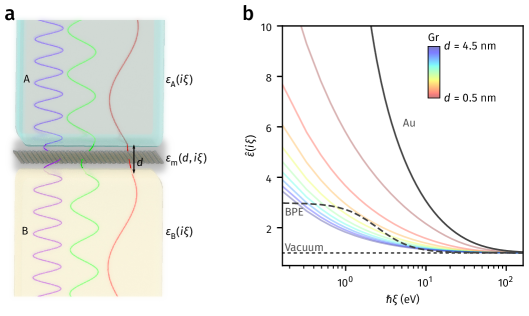
Consider two semi-infinite bulk materials A and B separated by a gap containing a sheet of monolayer 2D material (Fig. 1a). When the separation is larger than the vdW thickness of monolayer, we treat the separating gap containing the monolayer surrounded by vacuum as an effective birefringent medium with distinct in-plane (IP) and out-of-plane (OP) dielectric responses and , which are functions of and imaginary frequency , respectively, resulted from the different IP and OP electronic properties of the monolayer. Using the polarizability theory of 2D materials[25], and are given by and , where and are the -independent IP and OP polarizabilities for the 2D material extracted from first principle calculations, respectively (for details see Methods).
The vdW interaction potential between A and B across a birefringent medium m, , is given by[2] (for details see Methods):
| (2) |
where is the Boltzmann constant, is the absolute temperature, is the n-th Matsubara frequency, is the reduced Planck constant, is the retardation factor[2], is the speed of light in vacuum and is a dimensionless auxiliary variable. and are the geometrically-averaged dielectric function and dielectric anisotropy[25] of m, respectively. Similar approach was also used to calculate vdW interactions of layered materials[26]. and correspond to the dielectric mismatches following , for j = A, B. Analogous to inequality (1), the vdW potential for a given EM mode becomes positive when , contributing to vdW repulsion.
Using graphene (Gr), the thinnest carbon-based 2D material, as a model system, the calculated as a function of for different separations are shown in Fig. 1b. The dielectric responses have the same order of magnitude with those for high-refractive-index fluids[9, 10, 17] (Supplementary Fig. LABEL:si-fig:eps-cascade-full) but the applicable separation appears to be significantly smaller. Indeed, equation (2) suggests that the vdW repulsion can be tuned by the separation and the dielectric anisotropy , which highlight the versatility of 2D materials-mediated systems. Fig. 1b also includes the dielectric responses for the three bulk materials considered in our experiments later, including gold (Au), N,N’-bis(2-phenylethyl)perylene-3,4,9,10-bis(dicarboximide) (BPE)[27, 28] molecular solid, and vacuum (Vac). It reveals that vdW repulsion may be observed in two sets of materials, A/m/B = Vac/Gr/Au and Au/Gr/BPE, in which the former obeys inequality (1) in all separations and frequencies and the latter for separations nm.
As pointed out in several theoretical studies[26, 22], for an A/m/B system where m is a layer of 2D material, the total vdW potential consists of both attractive and repulsive contributions. Taking the Vac/Gr/Au system as an example, the gold layer on freestanding graphene is expected to not only experience a repulsive potential, , but also an attractive potential, , corresponding to the two-body vdW potential between gold and graphene, . The total potential acting on gold, , combines both effects. Our calculations based on equation (2) show that is of relatively longer-range, scaling as to , for separations from 1 nm to 10 nm, as compared to scaling as to (Fig. 2a). As a result, for nm, the first derivative of is positive, thereby yielding a net repulsive force between gold and vacuum through monolayer graphene.
According to our theoretical prediction, we carried out direct measurement for the vdW force experienced by a gold-coated tip in atomic force microscopy (AFM) interacting with a sheet of freestanding graphene (Fig. 2b). The freestanding graphene was fabricated by transferring a piece of micro-mechanically-exfoliated graphene to a holey silicon nitride (SiNx) membrane supported by a silicon chip [29], with the hole diameter of approximately 5 m, followed by annealing it in Ar/H2 to remove contaminants [30, 31]. A gold-coated AFM tip with a measured radius of 33 nm was chosen for the force-distance measurements (for details see Supplementary Section LABEL:si-sec:methods). All measurements were carried out in air. Supplementary Figs LABEL:si-fig:single-f-da and LABEL:si-fig:single-f-db show representative force-distance responses for the approach/retraction processes on freestanding and SiNx-supported graphene, respectively (measurement details see Supplementary Section LABEL:si-sec:F-d-meas). Note that when establishing the contact, the force response is quadratic for freestanding graphene, in contrast to the linear response on supported region. This is expected considering the mechanical flexibility of freestanding graphene membrane, which yields elastic response of higher order [32]. Indeed, during the retraction process from a freestanding graphene surface, the tip remains to adhere to graphene at a large tip displacement, revealing that both graphene and AFM cantilever were bent before overcoming the attractive two-body interaction . With the nonideality in mind, hereafter, we focus on the approach responses before physical contact with the sample surface.
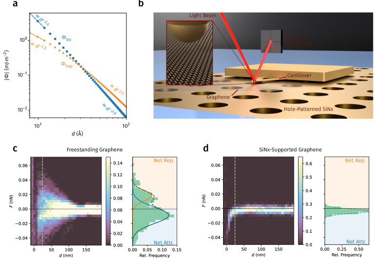
Figs 2c and 2d compare the two-dimensional histograms for the force-distance responses extracted from 225 and 36 measurements on freestanding and SiNx-supported graphene, respectively. The right panels present the force distributions at 24 nm corresponding to the green dashed lines on the two-dimensional histograms. Remarkably, more than 90 measurements showed repulsive behavior (representative response in Supplementary Fig. LABEL:si-fig:AFM-E-barrier-estimate). The force distribution on freestanding graphene (2c) is bimodal, which can be nicely decomposed to two Gaussian functions, revealing one population located at the repulsive regime (mean force = 18.2 pN and standard deviation = 7.2 pN). The attractive population ( = -8.7 pN and = 11.3 pN) presumably comes from the responses characterized on the area contaminated by airborne adsorbates [30], as well as the impurities introduced in process history, including transfer and scanning electron microscopy [33]. On the other hand, measurements on supported graphene (Fig. 2d) only yield attractive responses ( = -3.7 pN and = 3.0 pN). The theoretical picture presented in Fig. 2a suggests that the directly measured repulsive force corresponds to the forced required to overcome the repulsive energy barrier before the short-range attractive interaction overtakes. Given the tip radius characterized in SEM (33 nm), we calculated the height of repulsive energy barrier by integrating the average force response in the repulsive population with respect to , yielding a value of 195 Jm-2 (see Supplementary Section LABEL:si-sec:barrier-estimate), which nicely agrees with our theoretical prediction (20 Jm-2; see Supplementary Fig. LABEL:si-fig:lifshitz-barrier).
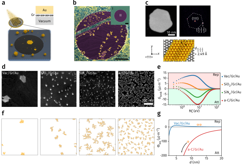
We have found that the vdW repulsion generated in Vac/Gr/Au system is sufficiently strong to alter the epitaxial properties of Au grown on freestanding graphene. As schematically shown in Fig. 3a, we evaporated a small amount ( ng·mm-2) of gold that condensed on a sheet of freestanding graphene in high vacuum at room temperature (for details see Methods). Fig. 3b shows a representative scanning electron micrograph (SEM) for gold deposited on graphene. Two regions, namely amorphous carbon (a-C) grid-supported (I) and freestanding (II) graphene, can be identified in the inset SEM image. The morphology and density for the deposited gold clusters on regions I and II exhibit substantially different features. On region I, as expected, due to a very high surface energy of gold ( mJ·m-2 at room temperature[34]), fast condensation at room temperature yields small spherical nanoclusters with a high nucleation density. However, on region II, despite a high degree of supercooling, the nucleation density is very low, leaving a large non-wettable area of up to 1.3 m2, with a few large and ultrathin gold platelets grown on the surface. We performed crystallographic analysis using the Fourier-transformed scanning transmission electron microscopy (FT-STEM) on a representative hexagonal platelet (Fig. 3c). A set of Bragg diffraction spots corresponding to {} lattice planes (lattice spacing of 2.49 Å) was observed, which was only reported in the atomically-thin face-center-cubic metal crystals[35]. We also notice that gold deposited on the defective and contaminated domains of freestanding graphene, e.g., region III, exhibits similar behavior with that on region I.
From a thermodynamic point of view, the growth of ultrathin gold platelets on freestanding graphene would require the Au-Gr interactions to be stronger than Au surface energy, or even a negative interfacial tension [36], which is unlikely and cannot explain the observed ultralow nucleation density. We further transferred graphene onto two other substrates, silicon oxide (SiO2) and silicon nitride (SiNx), and compared the morphologies of gold condensed on top (Fig. 3d). Fig. 3e presents the calculated many-body vdW interaction spectra as a function of energy, (see equation (2)), for the four systems considered here. The full-spectrum summation indicates that in contrast to the repulsive Vac/Gr/Au system, for SiO2/Gr/Au, SiNx/Gr/Au, and a-C/Gr/Au, the vdW interactions become increasingly attractive. Together with Fig. 3d, it becomes evident that stronger vdW repulsion would lead to lower nucleation density. The growth behavior is kinetically controlled which agrees with morphological statistics of the gold nanoplatelets based on AFM and SEM analysis (for details see Supplementary Section LABEL:si-sec:frict-diff-au). We further exclude the scenario of remote epitaxy[23] or “lattice transparency”[37] of graphene, since the highest crystalline samples were obtained on freestanding graphene, contradicting the polarity-dominated mechanism of remote epitaxy[24](more discussions see Supplementary Section LABEL:si-sec:effect-latt-transp).
density is proportional to , where Indeed, the classical nucleation theory suggests that the nucleation is the surface diffusivity[38]. According to the SEM images in Fig. 3d, we estimate that, by making graphene freestanding, the surface diffusivity of gold was boosted by up to approximately 9 orders of magnitude (Supplementary Fig. LABEL:si-fig:support-density, right -axis), indicating ultrafast in-plane diffusion. The platelets grown on freestanding graphene can be over times larger than that on a-C/Gr, indicating that the platelet growth is dominated by kinetic effect rather than thermodynamic wettability. The observation is further endorsed by our kinetic Monte Carlo (KMC) simulations considering the competition between Au diffusion on graphene and Au-Au binding processes on a surface (Fig. 3f and Supplementary Fig. LABEL:si-fig:kmc-theory-energy). Large and sparsely distributed platelets can only be obtained when the activation energy for diffusion is negligible compared to that for Au-Au binding (see Supplementary Section LABEL:si-sec:kmc-simulations-au).
The repulsive potential predicted by the Lifshitz model not only makes the surface adsorption an energy uphill process at large separation, but also decreases the vdW potential well depth at the contact distance by nearly 50% (Supplementary Fig. LABEL:si-fig:lifshitz-barrier), which further decrease the adsorption rate of gold onto freestanding graphene as predicted by classical aggregation theory[39]. As such, the vdW repulsion-induced energy barrier created above the surface offers a “highway” for in-plane diffusion (Fig. 3g), forming large platelets.
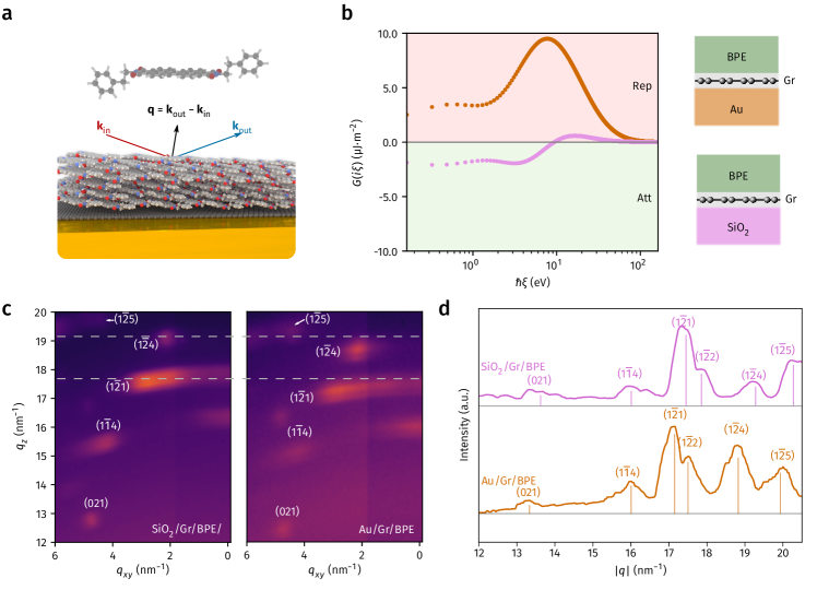
The second set of materials examined here is Au/Gr/BPE (Fig. 4a). The BPE molecule has a flat polycyclic aromatic core, perylenetetracarboxylic diimide (PTCDI), decorated with two freely rotatable phenylethyl groups on both ends. Highly ordered BPE molecular solids are of layered crystalline structure[28], with the interlayer spacing determined by the sensitive balance between intermolecular interactions of PTCDI cores and phenylethyl groups conformational entropy[40]. We therefore hypothesized that, by orienting the BPE molecular plane parallel to graphene, the force exerted by the substrate across graphene may alter the interlayer spacing.
The BPE molecules were thermally evaporated onto graphene supported by gold as well as SiO2 for comparison (Fig. 4b, for details see Methods). Fig. 4b presents the calculated for the two systems at nm. Following earlier discussion in Fig. 1b, for nm, the vdW potentials between Au and BPE are always repulsive irrespective of frequency, with the main contribution from the visible to ultraviolet region. The full-spectrum summation of according to equation (2) yields a strong vdW repulsion of 1.3 mJ·m-2. On the other hand, in SiO2/Gr/BPE system, the transition from attraction to repulsion at high frequencies leads to a weakly attractive potential (-20 J·m-2).
To examine the substrate interactions through graphene, we analyzed the molecular orientation and crystallographic constants of BPE molecular solids using synchrotron grazing-incidence wide-angle x-ray scattering (GIWAXS). In the GIWAXS patterns (Fig. 4c and Supplementary Fig. LABEL:si-fig:gixd-full-scale), both systems show several intense high-angle Laue spots, in particular those corresponding to the interlayer () and () planes (detailed crystallographic analysis see Supplementary Section LABEL:si-sec:molec-epit-bpe) near the axis, confirming the PTCDI plane is preferentially oriented parallel to the substrate [41, 42]. However, the slightly shifted components reveal polymorphs induced by the substrate force (Fig. 4c). The strongly repulsive substrate, gold, yielded interlayer spacings of 3.35 and 3.68 Å, respectively, which are enlarged by 1.8% as compared to the SiO2 control. The integrated line cuts extracted from GIWAXS patterns (Fig. 4d) compares the signals for SiO2/Gr/BPE and Au/Gr/BPE. The vdW repulsion generated in Au/Gr/BPE appears to slightly offset the interlayer interactions between BPE molecules. Consequently, the effect of phenylethyl groups conformational entropy takes a more active role, increasing the interlayer spacing for a set of high- diffraction peaks (, , , and ) associated with the PTCDI basal plane. Further experimental examination of molecular packing on graphene-free substrates indicates the breakdown of classical vdW transparency theory in this system (more details see Supplementary Sections LABEL:si-sec:breakd-wett-transp and LABEL:si-sec:effect-latt-transp).
We have presented direct force measurement of the vdW repulsion at 2D materials surfaces and demonstrated that the vdW repulsion can substantially influence kinetics and thermodynamics of heteroepitaxy. Our findings imply that the recently reported quantum levitation [9, 11, 16] might be even realized without liquid immersion, which give rise to robust solid-state device miniaturization. In addition, in view of the growth of 2D materials family covering an increasingly large range of properties, they could become versatile surface coatings selectively repelling objects down to atomic level, which may lead to new molecular mechanical systems and sensors.
Author Contributions
T.T., G.V. and C.J.S. conceived the idea and designed the experiments. T.T. and F.N. developed the theoretical framework. T.T. performed first-principle calculations under guidance of E.J.G.S. G.V. carried out AFM force measurement, analyzed the data, and modeled the force responses. T.T., G.V. and K.C. fabricated the freestanding graphene samples and carried out Au deposition. T.T characterized the freestanding graphene samples. F.K. performed STEM measurements. T.T. carried out KMC simulations. T.T. transferred graphene onto gold and SiO2 substrates. Y.T.L and S.W.C. deposited BPE molecules and carried out synchrotron GIWAXS under supervision of Y.C.C. T.T., Y.T.L. and Y.C.C. analyzed the GIWAXS patterns. T.T., G.V. and C.J.S. co-wrote the paper. All authors contributed to this work, read the manuscript, discussed the results, and agreed to the contents of the manuscript and supplementary materials.
Acknowledgments
C.J.S. is grateful for financial support from ETH startup funding and the European Research Council Starting Grant (N849229 CQWLED). T.T. G.V. and K.C. acknowledge technical support from the Scientific Center for Optical and Electron Microscopy (ScopeM) and FIRST-Center for Micro- and Nanoscience of ETH Zurich. EJGS acknowledges computational resources through the UK Materials and Molecular Modeling Hub for access to THOMAS supercluster, which is partially funded by EPSRC (EP/P020194/1); CIRRUS Tier-2 HPC Service (ec131 Cirrus Project) at EPCC (http://www.cirrus.ac.uk) funded by the University of Edinburgh and EPSRC (EP/P020267/1); ARCHER UK National Supercomputing Service (http://www.archer.ac.uk) via d429 Project code, and the UKCP consortium (Project e89) funded by EPSRC grant ref EP/P022561/1. EJGS also acknowledges the EPSRC Early Career Fellowship (EP/T021578/1) and the University of Edinburgh for funding support. Y.C.C. thanks the financial support by the “Advanced Research Center for Green Materials Science and Technology” from The Featured Area Research Center Program within the framework of the Higher Education Sprout Project by the Ministry of Education (108L9006) and the Ministry of Science and Technology in Taiwan (MOST 108-3017-F-002-002 and 108-2221-E-011-047). T.T. thanks Dr. Liqing Zheng for providing gold substrates.
Supplementary materials
-
•
Materials and Methods
-
•
Supplementary Text
-
•
Figs. S1 to S34
-
•
Tables S1 to S4
-
•
References (S1-S46)
References
- [1] L.. Woods et al. “Materials perspective on Casimir and van der Waals interactions” In Rev. Mod. Phys. 88.4 American Physical Society (APS), 2016, pp. 045003 DOI: 10.1103/revmodphys.88.045003
- [2] V. Parsegian “Van der Waals Forces: A Handbook for Biologists, Chemists, Engineers, and Physicists”, 2010 DOI: 10.1017/CBO9780511614606
- [3] Hendrick BG Casimir “On the attraction between two perfectly conducting plates” In K. Ned. Akad. Wet. 51, 1948, pp. 793–795
- [4] H… Casimir and D. Polder “The Influence of Retardation on the London-van der Waals Forces” In Phys. Rev. 73.4 American Physical Society (APS), 1948, pp. 033001 DOI: 10.1103/physrev.73.360
- [5] WH Keesom “The second viral coefficient for rigid spherical molecules, whose mutual attraction is equivalent to that of a quadruplet placed at their centre” In Proc. R. Acad. Sci 18, 1915, pp. 636–646
- [6] Geoffrey C Maitland “Intermolecular forces: their origin and determination” Oxford University Press, 1981
- [7] F. London “The general theory of molecular forces” In Trans. Faraday Soc. 33 Royal Society of Chemistry (RSC), 1937, pp. 8b–26 DOI: 10.1039/tf937330008b
- [8] I E Dzyaloshinskii, E M Lifshitz and Lev P Pitaevskii “General Theory of van der Waals’ Forces” In Phys.-Uspekhi 4.2 IOP Publishing, 1961, pp. 153–176 DOI: 10.1070/pu1961v004n02abeh003330
- [9] J.. Munday, Federico Capasso and V. Parsegian “Measured long-range repulsive Casimir–Lifshitz forces” In Nature 457.7226 Springer ScienceBusiness Media LLC, 2009, pp. 170–173 DOI: 10.1038/nature07610
- [10] Adam A. Feiler, Lennart Bergström and Mark W. Rutland “Superlubricity Using Repulsive van der Waals Forces” In Langmuir 24.6 American Chemical Society (ACS), 2008, pp. 2274–2276 DOI: 10.1021/la7036907
- [11] Rongkuo Zhao et al. “Stable Casimir equilibria and quantum trapping” In Science 364.6444 American Association for the Advancement of Science (AAAS), 2019, pp. 984–987 DOI: 10.1126/science.aax0916
- [12] Tao Gong et al. “Recent progress in engineering the Casimir effect – applications to nanophotonics, nanomechanics, and chemistry” In Nanophotonics 10.1, 2021, pp. 523–536 DOI: doi:10.1515/nanoph-2020-0425
- [13] Andrew Milling, Paul Mulvaney and Ian Larson “Direct Measurement of Repulsive van der Waals Interactions Using an Atomic Force Microscope” In J. Colloid Interface Sci. 180.2 Elsevier BV, 1996, pp. 460–465 DOI: 10.1006/jcis.1996.0326
- [14] Anders Meurk, Paul F. Luckham and Lennart Bergström “Direct Measurement of Repulsive and Attractive van der Waals Forces between Inorganic Materials” In Langmuir 13.14 American Chemical Society (ACS), 1997, pp. 3896–3899 DOI: 10.1021/la9610967
- [15] Seung-woo Lee and Wolfgang M. Sigmund “AFM study of repulsive van der Waals forces between Teflon AF™ thin film and silica or alumina” In Colloids Surf. A 204.1-3 Elsevier BV, 2002, pp. 43–50 DOI: 10.1016/s0927-7757(01)01118-9
- [16] J.. Munnday and Federico Capasso “Repulsive Casimir and van der Waals Forces: From Measurements to Future Technologies” In Int. J. Mod. Phys. A 25.11 World Scientific Pub Co Pte Lt, 2010, pp. 2252–2259 DOI: 10.1142/s0217751x10049529
- [17] Mathias Boström, Bo E. Sernelius, Iver Brevik and Barry W. Ninham “Retardation turns the van der Waals attraction into a Casimir repulsion as close as 3 nm” In Phys. Rev. A 85.1 American Physical Society (APS), 2012, pp. 010701 DOI: 10.1103/physreva.85.010701
- [18] Javad Rafiee et al. “Wetting transparency of graphene” In Nat. Mater. 11.3 Springer ScienceBusiness Media LLC, 2012, pp. 217–222 DOI: 10.1038/nmat3228
- [19] Chih-Jen Shih et al. “Breakdown in the Wetting Transparency of Graphene” In Phys. Rev. Lett. 109.17 American Physical Society (APS), 2012, pp. 176101 DOI: 10.1103/physrevlett.109.176101
- [20] Musen Li, Jeffrey R. Reimers, John F. Dobson and Tim Gould “Faraday cage screening reveals intrinsic aspects of the van der Waals attraction” In Proc. Nat. Acad. Sci. 115.44, 2018, pp. E10295–E10302 DOI: 10.1073/pnas.1811569115
- [21] Xiaofei Liu, Zhuhua Zhang and Wanlin Guo “van der Waals screening by graphenelike monolayers” In Phys. Rev. B 97.24 American Physical Society (APS), 2018, pp. 241411 DOI: 10.1103/physrevb.97.241411
- [22] Alberto Ambrosetti and Pier Luigi Silvestrelli “Hidden by graphene – Towards effective screening of interface van der Waals interactions via monolayer coating” In Carbon 139 Elsevier BV, 2018, pp. 486–491 DOI: 10.1016/j.carbon.2018.07.011
- [23] Yunjo Kim et al. “Remote epitaxy through graphene enables two-dimensional material-based layer transfer” In Nature 544.7650 Springer ScienceBusiness Media LLC, 2017, pp. 340–343 DOI: 10.1038/nature22053
- [24] Wei Kong et al. “Polarity governs atomic interaction through two-dimensional materials” In Nat. Mater. 17.11 Springer Nature, 2018, pp. 999–1004 DOI: 10.1038/s41563-018-0176-4
- [25] Tian Tian et al. “Electronic Polarizability as the Fundamental Variable in the Dielectric Properties of Two-Dimensional Materials” In Nano Lett. 20.2 American Chemical Society (ACS), 2019, pp. 841–851 DOI: 10.1021/acs.nanolett.9b02982
- [26] Yao Zhou, Lenson A Pellouchoud and Evan J Reed “The potential for fast van der Waals computations for layered materials using a Lifshitz model” In 2D Mater. 4.2 IOP Publishing, 2017, pp. 025005 DOI: 10.1088/2053-1583/aa528e
- [27] J. Mizuguchi “N,N’-Bis(2-phenethyl)perylene-3,4:9,10-bis(dicarboximide)” In Acta Cryst. C 54.10 International Union of Crystallography (IUCr), 1998, pp. 1479–1481 DOI: 10.1107/s0108270198005575
- [28] M.-M. Ling et al. “Air-Stable n-Channel Organic Semiconductors Based on Perylene Diimide Derivatives without Strong Electron Withdrawing Groups” In Adv. Mater. 19.8 Wiley, 2007, pp. 1123–1127 DOI: 10.1002/adma.200601705
- [29] Grégory F. Schneider et al. “Wedging Transfer of Nanostructures” In Nano Lett. 10.5, 2010, pp. 1912–1916 DOI: 10.1021/nl1008037
- [30] Zhiting Li et al. “Effect of airborne contaminants on the wettability of supported graphene and graphite” In Nat. Mater. 12.10 Springer ScienceBusiness Media LLC, 2013, pp. 925–931 DOI: 10.1038/nmat3709
- [31] Christopher J Russo and Lori A Passmore “Controlling protein adsorption on graphene for cryo-EM using low-energy hydrogen plasmas” In Nat. Methods 11.6 Springer ScienceBusiness Media LLC, 2014, pp. 649–652 DOI: 10.1038/nmeth.2931
- [32] Changgu Lee, Xiaoding Wei, Jeffrey W. Kysar and James Hone “Measurement of the Elastic Properties and Intrinsic Strength of Monolayer Graphene” In Science 321.5887, 2008, pp. 385–388 DOI: 10.1126/science.1157996
- [33] D. Teweldebrhan and A.. Balandin “Modification of graphene properties due to electron-beam irradiation” In Appl. Phys. Lett. 94.1, 2009, pp. 013101 DOI: 10.1063/1.3062851
- [34] K.. Mills and Y.. Su “Review of surface tension data for metallic elements and alloys: Part 1 – Pure metals” In Int. Mater. Rev. 51.6 Informa UK Limited, 2006, pp. 329–351 DOI: 10.1179/174328006x102510
- [35] Rongchao Jin et al. “Photoinduced Conversion of Silver Nanospheres to Nanoprisms” In Science 294.5548 American Association for the Advancement of Science (AAAS), 2001, pp. 1901–1903 DOI: 10.1126/science.1066541
- [36] Jacob N. Israelachvili “Intermolecular and surface forces” Amsterdam: Elsevier, Academic Press, 2011
- [37] Sieun Chae et al. “Lattice Transparency of Graphene” In Nano Lett. 17.3 American Chemical Society (ACS), 2017, pp. 1711–1718 DOI: 10.1021/acs.nanolett.6b04989
- [38] Y.. Mo, J. Kleiner, M.. Webb and M.. Lagally “Activation energy for surface diffusion of Si on Si(001): A scanning-tunneling-microscopy study” In Phys. Rev. Lett. 66.15 American Physical Society (APS), 1991, pp. 1998–2001 DOI: 10.1103/physrevlett.66.1998
- [39] N Fuchs “Zur theorie der koagulation” In Z. Phys. Chem. 171.1 De Gruyter, 1934, pp. 199–208
- [40] Rüdiger Schmidt et al. “High-Performance Air-Stable n-Channel Organic Thin Film Transistors Based on Halogenated Perylene Bisimide Semiconductors” In J. Am. Chem. Soc. 131.17 American Chemical Society (ACS), 2009, pp. 6215–6228 DOI: 10.1021/ja901077a
- [41] Yu-Cheng Chiu et al. “Multilevel nonvolatile transistor memories using a star-shaped poly((4-diphenylamino)benzyl methacrylate) gate electret” In NPG Asia Mater. 5.2 Springer ScienceBusiness Media LLC, 2013, pp. e35 DOI: 10.1038/am.2012.64
- [42] Chih-Jen Shih et al. “Partially-Screened Field Effect and Selective Carrier Injection at Organic Semiconductor/Graphene Heterointerface” In Nano Lett. 15.11 American Chemical Society (ACS), 2015, pp. 7587–7595 DOI: 10.1021/acs.nanolett.5b03378