ALIGN: A System for Automating Analog Layout ††thanks: This work was supported by the DARPA IDEA program under SPAWAR contract N660011824048.
Abstract
ALIGN (“Analog Layout, Intelligently Generated from Netlists”) is an open-source automatic layout generation flow for analog circuits. ALIGN translates an input SPICE netlist to an output GDSII layout, specific to a given technology, as specified by a set of design rules. The flow first automatically detects hierarchies in the circuit netlist and translates layout synthesis to a problem of hierarchical block assembly. At the lowest level, parameterized cells are generated using an abstraction of the design rules; these blocks are then assembled under geometric and electrical constraints to build the circuit layout. ALIGN has been applied to generate layouts for a diverse set of analog circuit families: low frequency analog blocks, wireline circuits, wireless circuits, and power delivery circuits.
1 Motivation and Goals
ALIGN (Analog Layout, Intelligently Generated from Netlists) is an open-source layout generator for analog circuits that is currently under development. The release date for Version 1 of the software flow is in August 2020. The ALIGN project engages a joint academic/industry team to translate a SPICE-level netlist into a physical layout, with 24-hour turnaround and no human in the loop. The ALIGN flow inputs a netlist whose topology and transistor sizes have already been chosen, specifications, and a process design kit (PDK), and outputs GDSII.
The philosophy of ALIGN is to compositionally synthesize the layout by first identifying layout hierarchies in the netlist, then generating correct-by-construction layouts at the lowest level of hierarchy, and finally assembling blocks at each level of hierarchy during placement and routing. Thus, a key step in ALIGN is to identify these hierarchies to recognize the building blocks of the design. In doing so, ALIGN mimics the human designer, who identifies known blocks, lays them out, and then builds the overall layout hierarchically. At the lowest level of this hierarchy is an individual transistor; these transistors are then combined into larger fundamental primitives (e.g., differential pairs, current mirrors), then modules (e.g., operational transconductance amplifiers (OTAs)), up through several levels of hierarchy to the system level (e.g., an RF transceiver). ALIGN uses a mix of algorithmic techniques, template-driven design, and machine learning (ML) to create layouts that are at the level of sophistication of the expert designer.
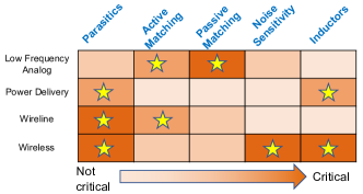
Unlike digital designs that are built from a composition of a small number of building blocks, analog circuits tend to use a wide variety of structures. Each of these has its own constraints and requirements, and traditionally only the expert designer has been able to build circuits that could deliver high performance. ALIGN targets a wide variety of analog designs, in both bulk and FinFET technologies, covering four broad classes of functionality:
-
•
Low-frequency components that include analog-to-digital converters (ADCs), amplifiers, and filters.
-
•
Wireline components that include clock/data recovery, equalizers, and phase interpolators.
-
•
RF/Wireless components that implement transmitters, receivers, etc.
-
•
Power delivery components include capacitor- and inductor-based DC-to-DC converters.
Each class is characterized by similar building blocks that may have a similar set of performance parameters, although it should be mentioned that there is considerable diversity even within each class. An overview of factors that are important in the design for each category is summarized in Fig. 1.
There have been several prior efforts to automate analog layout synthesis [1, 2, 3, 4, 5, 6, 7], but these methods are not widely deployed in tools today. Some methods address limited classes of designs; others cannot be tuned to handle a wide enough set of variants of the same design class. Moreover, there is a general consensus that prior methods for automating analog layout have been unable to match the expert designer, both in terms of the ability to comprehend and implement specialized layout tricks, and the number and variety of topologies with circuit-specific constraints. The ultimate goal for analog layout synthesis is to match the quality of a hand-crafted design.
In recent years, the landscape has shifted in several ways, making automated layout solutions attractive. First, in nanometer-scale technologies, restricted design rules with fixed pitches and unidirectional routing limit the full freedom for layout that was available in older technologies, thus reducing the design space to be explored during layout, reducing the advantage to the human expert. Second, today more analog blocks are required in integrated systems than before, and several of these require correct functionality and modest performance. The combination of increasing analog content with the relaxation in specifications creates a sweet spot for analog automation. Even for high-performance blocks, an automated layout generator could considerably reduce the iterations between circuit optimization and layout, where layout generation is the primary bottleneck. Third, the advent of ML provides the promise for attacking the analog layout problem in a manner that was not previously possible, and set the stage for no-human-in-the-loop design.
This article provides an overview of the technical details of ALIGN and shows how ALIGN has been used to translate analog circuit netlists to layouts. The core ALIGN engine can be run with no human in the loop, enabled by ML algorithms that perform the functions typically performed by humans, e.g., recognizing hierarchies in the circuit during auto-annotation, or generating symmetry constraints for layout. ML algorithms can also be instrumental in creating rapid electrical constraint checkers, which verify whether a candidate placement/routing solution meets performance constraints or not, and using this to guide the place-and-route engine towards optima that meet all specification. For deeper details, the reader is referred to detailed descriptions in [8, 9, 10, 11], and to watch for new publications of ongoing work by our group.
2 The Technical Core of ALIGN
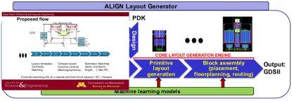
The ALIGN flow consists of five modules, illustrated in
Fig. 2:
(1) Netlist auto-annotation creates a multilevel hierarchical representation
of the input netlist and identifies structural symmetries in the netlist. This is
a key step that is used to hierarchically build the layout of the circuit.
(2) Design rule capture abstracts the proprietary PDK into a simplified grid,
appended with Boolean constraints as needed, that must be obeyed at all steps
during layout.
(3) Constraint generation identifies the performance constraints
to be met, and transforms them into layout constraints, such as maximum
allowable net lengths, or constraints such as matching/common-centroid based on
structural information identified during auto-annotation.
(4) Parameterized primitive cell generation automatically builds layouts for
primitives, the lowest-level blocks in the ALIGN hierarchy. Primitives
typically contain a small number of transistor structures (each of which may be
implemented using multiple fins and/or fingers). A parameterized instance of a
primitive in the netlist is automatically translated to a GDSII layout in this step.
(5) Hierarchical block assembly performs placement and routing on the
hierarchical circuit structure while meeting geometric and electrical
constraints.
The flow creates a separation between open-source code and proprietary data.
Proprietary PDK models must be translated into an abstraction that is used by
the layout generators. Parts of the flow are driven by ML models: the
flow provides infrastructure for training these models on proprietary data.
The overall ALIGN flow is intended to support no-human-in-the-loop design. However, the flow is modular and supports multiple entry points: for example, the auto-annotation module could be replaced by designer annotation, and the rest of the flow could be executed using this annotation. The flow is flexible to user input: for example, the user can specify new primitives, and they will be used by the annotation module as well as the layout generator within the flow.
2.1 Netlist Auto-Annotation
This step groups transistors and passives in the input netlist into a hierarchical set of building blocks and identifies constraints on the layout of each block. The input to ALIGN is a SPICE netlist that is converted to a graph representation. Next, features of the graph are recognized, and a circuit hierarchy is created. If the input netlist is partitioned into subcircuits, such information is used during recognition, but ALIGN does not count on netlist hierarchy. Instead, hierarchies are automatically identified and annotated. It is important to note that the best layout hierarchy may sometimes differ from a logical netlist hierarchy; hence, ALIGN may flatten netlist hierarchies to build high-quality layouts.
Analog designers typically choose from a large number for variants of each design block, e.g., between textbooks and research papers, there are well over 100 widely used OTA topologies of various types (e.g., telescopic, folded cascode, Miller-compensated). Prior methods are library-based (i.e., they match a circuit to prespecified templates) [4] or knowledge-based (i.e., they determine block functionality using a set of encoded rules) [1], or both [12]. Library-based methods require a large library, while rule-based methods must be supported by an exhaustive knowledge base, both of which are hard to build and maintain. ALIGN uses two approaches for annotating circuits blocks, both based on representing the circuit connectivity using a graph representation:
Machine learning based methods: For commonly encountered blocks, the problem of identifying blocks maps on to whether a subgraph of the larger circuit is isomorphic to a known cell. However, to allow for design variants, ALIGN uses approximate graph isomorphism, enabled by the use of graph convolutional neural networks (GCNs) that classify nodes within the circuit graph into classes (e.g., OTA nodes, LNA nodes, Mixer nodes). With some minimal postprocessing, it is demonstrated that this approach results in excellent block recognition. Details of the approach are provided in [8]. A training set for the GCN, consisting of 1390 OTA circuits, including bias networks, is available on the ALIGN GitHub repository.
Graph traversal based methods: It is unrealistic to build a training set that covers every possible analog block, and for blocks that lie outside the scope of the GCN training set, we use graph-based approaches to recognize repeated structures within a circuit. Such structures typically require layout constraints: for example, analog-to-digital converters may use a set of binary weighted capacitors or a set of resistors in an R-2R ladder, and these require careful placement in common-centroid fashion and symmetric routing. ALIGN employs methods based on graph traversal and approximate subgraph isomorphism to recognize these array structures.
Once these structures are recognized in a very large circuit graph, they form a level of hierarchy. Within these blocks, lower hierarchical levels can be detected using conventional subgraph isomorphism methods: sub-blocks at these levels have fewer variants and can be efficiently recognized using library-based approaches.
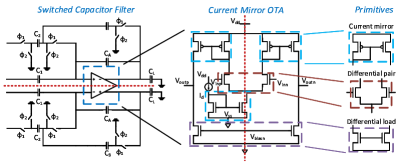
Fig. 3 shows the results of auto-annotation on a switched-capacitor filter. A GCN-based approach can be used to identify the current-mirror OTA, and then primitives within the OTA can be identified. In the process, lines of symmetry within each structure can be found, as illustrated in the figure. At the primitive level, since the layouts are generated by the parameterized cell generator, these lines of symmetry are implicit in the definition of the primitive. At higher levels, these can be inferred during auto-annotation.
2.2 Design Rule Abstraction
The ALIGN layout tools are guided by process-specific design rules that ensure DRC-correctness. The complexity of design rules has grown significantly in recent process generations. Efforts at building generalized abstractions for process rules have previously been proposed (e.g., [13]). ALIGN uses a more efficient design rule abstraction mechanism that creates fixed grid structures in FEOL and BEOL layers, as illustrated in Fig. 4. Major grids (bold lines), represent centerlines for routes, while minor grids (dashed lines) correspond to stopping points for features. The gridding structure and basic process information is abstracted into a JSON file. For BEOL layers, this includes:
-
•
default wire dimensions, pitch, and grid offset (Pitch, Width, MinL, MaxL, Offset).
-
•
end-to-end spacing design rules (EndToEnd).
-
•
metal direction, colors (Direction, Color).
-
•
via rules (Space{X/Y}, Width{X/Y}, VencA_{L/H}, VencP_{L,H}).
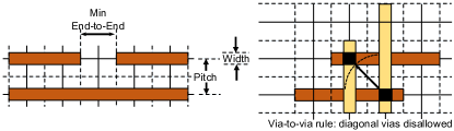
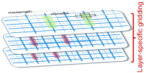
While this is superficially similar to traditional -rules, our abstraction permits a different gridding structure that can vary from layer to layer, and the use of major/minor grid lines that represent wire pitches, wire overhangs, as well as the ability to incorporate via rules through Boolean constraints. Our approach reduces the complex set of conditions embedded in thousands of rules in a design rule manual to a massively simplified and much smaller set, enforcing some limitations through the choice of grids. It is found, through comparisons with manual design, that this leads to minimal or zero degradation in layout quality. Advanced commercial process nodes (22nm, 10nm, 7nm, beyond) have been abstracted into this simplified form. The abstraction enables layout tools to comprehend PDK features such as regular and irregular width and spacing grids (for each layer), minimum end to end spacing design rules (between metals in the same track), minimum length design rules, and enforced stopping point grids. For convenience, the JSON file also encodes per unit parasitics for metal layers and vias.
To facilitate further layout research, we have released design rules for Mock PDKs based on public-domain information to abstract layout rules at a 14nm FinFET node [14] and a 65nm bulk node [15]. While they do not represent a real technology, they are realistic. Validation of the design tools on these PDKs, which can be freely shared, helps the software development process.
2.3 Constraint Generation
Two types of constraints are generated to guide layout:
Geometric constraints: As the auto-annotation step recognizes known blocks or array structures, it associates geometric requirements with these blocks, such as symmetry, matching, and common-centroid constraints. For instance, Fig. 3 shows lines of symmetry in an OTA structure that must be respected during layout. These constraints are extracted naturally as part of auto-annotation. In contrast with prior methods that are based on simulation-intensive sensitivity analysis [16] or graph traversal based exact matching to templates [4], the approach in ALIGN method [9] combines graph traversal methods with machine learning based methods and is computationally efficient, capable of finding hierarchically nested symmetry constraints even under approximate matches.
Electrical constraints: ALIGN generates a layout based on a fixed netlist, and performance shifts are driven by changes in parasitics from netlist-level estimates to post-layout values. Therefore, ALIGN translates electrical constraints to bound the maximum parasitics at any node of the circuit. For instance, an electrical constraint may be translated to a maximum limit on the resistance of a wire connecting two nodes, which in turn corresponds to a constraint on the maximum length, the number of parallel metal tracks, and the number of vias on the route connecting these nodes. This feature is currently being implemented in ALIGN [10, 11] and is a work in progress. The essential idea is to develop a fast ML inference engine that operates within the inner loop of an iterative placer, and for each placer configuration, determines whether or not its electrical constraints are satisfied.
These constraints are passed on to the layout generation engine to guide layout at all levels of hierarchy.
2.4 Parameterized Primitive Layout Generation
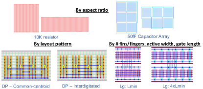
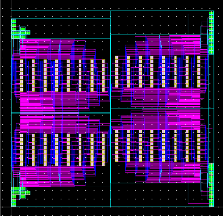
ALIGN provides the user with a predefined library of parameterizable primitives, as illustrated in Fig. 5. Each primitive consists of a small number of transistor or passive units; however, each such unit may consist of multiple replicated structures, such as multifin/multifinger transistors, or resistive/capacitive arrays.
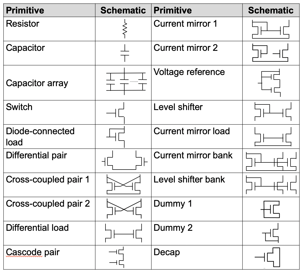
The primitive cell layout follows the gridded abstraction defined by the design rules, and cell generation can be parameterized in terms of the unit cell and the number of unit cells, as shown in Fig. 6. For a transistor, a unit cell may be parameterized by the number of fins in a FinFET technology; for a capacitor, parameterization may correspond to the size of the unit capacitor. Additionally, primitive layouts can be parameterized by their aspect ratio, their layout style (common-centroid vs. interdigitated transistors), the gate length, the effective widths of critical wires in the cell, etc.
The utility in recognizing primitives and creating parameterized layouts is in enabling ALIGN to create layouts that incorporate the appropriate geometric constraints (e.g., symmetry or common-centroid). In principle, a layout could be built using a “sea of transistors,” where the primitive corresponds to a single transistor, but it would be challenging for such an approach to enforce symmetry requirements beyond the transistor primitives. Prior methods for primitive layout generation [17, 18, 19, 20] have generally not been as modular or scalable as the ALIGN approach.
2.5 Hierachical Block Assembly
Given the layouts of all primitives and the hierarchical block level structure of the circuit, extracted during auto-annotation, the placement and routing step performs hierarchical block assembly that obeys the geometric and electrical constraints described earlier.
Each layout block in the hierarchy can have multiple layout options with different shapes generated for each module. For example, primitives can be parameterized by aspect ratio, and multiple aspect ratios for other blocks may be generated. Flexible shapes drive floorplanning-like placement algorithms that deliver compact layouts under the electrical and geometric constraints passed on to them by the constraint generation step. Routing is integrated into each hierarchical level, accounting for net length/parasitic constraints, shielding and symmetry requirements, and conforming with the design rules embedded into the PDK abstraction. The placer is based on prior work using the sequence pair method [6] and can handle general geometric constraints, such as symmetry, matching and alignment. Symmetry, shielding and resistance-constrained routing are supported during routing.
The ALIGN flow can employ one of two detailed routers: (a) A constructive router that uses an integer linear programming formulation and an A* algorithm; this works particularly well for more sparse designs. (b) A SAT-based detailed router111github.com/ALIGN-analoglayout/AnalogDetailedRouter, released by Intel, which is well suited for congested designs.
3 Working in an Open-source Environment
3.1 Why Open-source Software?
Aside from technical innovations, ALIGN breaks new ground in providing a fully open-source analog layout software, something that has not been available in the past. The availability of open-source software is crucial for nurturing future innovations in the field. First, further research can build upon a “piece of the puzzle” of analog layout design: for instance, a new cell generator can plug into the open-source ALIGN flow and show end-to-end results from netlist to layout, rather than providing limited results at the end of cell generation. Second, open-source enables a path to ensure that reported results can be reproducible. The traction for open-source is evidenced not only through the efforts in ALIGN, but also in other notable efforts on analog layout [21], digital layout (including back-end infrastructure such as parasitic extraction on power delivery that is more broadly applicable to any other class of design [22].
3.2 Open-source Designs
Unlike digital designs, where a wealth of designs exists in the public domain, the font of analog designs is very sparse. Design parameters tend to be closely linked with process nodes and existing automation flows do not allow robust circuit optimization to meet constraints. Sharing designs based on a commercial PDK over multiple institutions requires a multiway nondisclosure agreement involving the institutions, the foundry, and the foundry access provider. Within the ALIGN team, this issue was complicated by the need for such an agreement to cover both academic and industry team members.
The ALIGN GitHub repository hosts a number of sized analog netlists, a set that is growing, to facilitate open research. These netlists contain testbenches that measure the performance parameters of the circuit to verify its adherence to specifications. Moreover, as stated earlier, the repository contains unsized netlist topologies for a variety of OTA circuits.
3.3 Software Infrastructure
The software flow is maintained on a GitHub repository [23] and may be downloaded and installed in a native Linux environment. Alternatively, it may be run in a lightweight Docker container that performs operating system virtualization and enables portability and ease of maintenance. ALIGN can leverage the use of other open-source tools such as the KLayout layout viewer. The core software flow is Python-based, and the computationally intensive engines – notably the placer and router – are implemented in C++.
The project is aided by the use of tools that are vital to a open-source infrastructure with continuous integration (CI). These include CI build flows, using CircleCI, for automated build of new components as they are added to the repository; unit testing, using pytest, to verify the correctness of individual units of source code that is added to the repository; code coverage to measure how much of the code is executed by the automated tests, using coverage.py with Codecov for tracking; and automated code review for code quality checks using Codacy.
| Schematic | Manual layout | ALIGN Layout | |
| (RC extract) | (RC extract) | ||
| Gain (dB) | 24.28 | 24.22 | 24.14 |
| 3dB frequency (MHz) | 24 | 24 | 24 |
| UGF (MHz) | 199 | 197 | 198 |
| Phase margin (∘) | 89 | 88 | 88 |
| Input offset (mV) | 0 | 0.13 | 0.10 |
| Specification | Schematic | Manual layout | ALIGN layout |
|---|---|---|---|
| (RC extract) | (RC extract) | ||
| Gain (dB) | 16.1 | 15.84 | 15.59 |
| 3dB frequency (KHz) | 503 | 511 | 524 |
| Unity gain frequency (KHz) | 3435 | 3415 | 3610 |
| Input offset (mV) | 0 | 0.13 | 0.10 |
| SDC | Signal adder | |||
| Gain (dB) [Gain] | BW (GHz) [BW] | Gain (dB) [Gain] | BW (GHz) [BW] | |
| S | - | |||
| M | - [-] | [-] | [-%] | [-%] |
| A | - [-%] | [-] | [-%] | [-%] |
| VGA | Linear equalizer | |||
| Gain (dB) [Gain] | BW (GHz) [BW] | Gain (dB) [Gain] | BW (GHz) [BW] | |
| S | -dB | |||
| M | -dB [%] | [-%] | [-%] | [-%] |
| A | -dB [-%] | [-%] | [-%] | [-%] |
4 Results
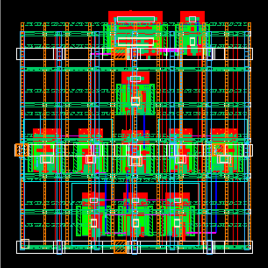
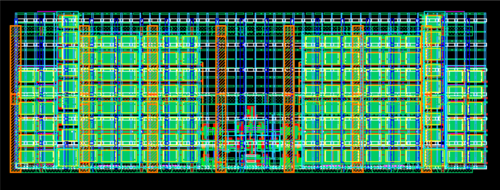
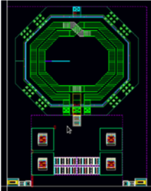
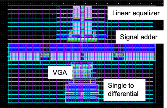
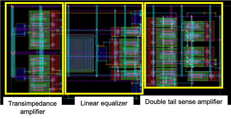
The ALIGN flow has been applied to generate layouts for circuits that lie in all four classes: low-frequency analog, wireline, wireless, and power delivery. We are unaware of a prior layout generator that has been demonstrated to handle such a broad class of circuits. Fig. 7 illustrates a sample set of layouts generated using ALIGN: these include a current-mirror OTA with bias circuitry and its power grid (Fig. 7(b)), a switched capacitor (SC) filter containing the OTA (Fig. 7(c)), an analog-to-digital converter [all low-frequency analog], a bandpass filter (Fig. 7(e)) [wireless], a switched capacitor DC-to-DC converter (Fig. 7(a)) [power delivery], and an equalizer (Fig. 7(f)) and an optical receiver (Fig. 7(g)) [both wireline]. The layouts are compact and regular.
A set of representative results for the post-layout performance analysis of ALIGN-generated layouts for the OTA (Fig. 7(b)) and the switched-capacitor filter (Fig. 7(c)) containing the OTA are shown in Tables I and II, respectively. For the larger block, the switched-capacitor filter, the extraction results show a good match with the schematic simulation (this level of mismatch between schematic and layout performance is quite normal in analog design), attesting to the quality of the layout. Moreover, the layout respects symmetry constraints that are considered important by analog designers to guard against parasitic mismatch due to systematic variability. For both layouts, the performance of the ALIGN-generated layout is very close to that of the manual layout.
For a set of wireline circuits, Table III shows a comparison between the performance of the ALIGN-generated layout and a hand-crafted manual layout, and shows that the performance of both layouts is comparable.
5 Conclusion
This paper summarizes the current state of the ALIGN flow for automated analog layout synthesis. ALIGN is open-source and may be downloaded and used freely [23]. Currently, the project has seen about 24 months of development, and can already synthesize layouts for a wide variety of analog circuits. It is expected that the capabilities of ALIGN will be enhanced significantly over the next few years, handling more sophisticated circuits, more complex constraints, and improved software robustness. The inherent hierarchical approach adopted by ALIGN is key to ensuring scalability of the software to larger designs in future, while also providing high-quality solutions.
References
- [1] R. Harjani, et al., “OASYS: A framework for analog circuit synthesis,” IEEE Transactions on Computer-Aided Design of Integrated Circuits and Systems, vol. 8, pp. 1247–1266, Dec. 1989.
- [2] J. Cohn, et al., “KOAN/ANAGRAM II: New tools for device-level analog placement and routing,” IEEE Journal of Solid-State Circuits, vol. 26, pp. 330–342, Mar. 1991.
- [3] H. E. Graeb, ed., Analog Layout Synthesis: A Survey of Topological Approaches. New York, NY: Springer, 2010.
- [4] M. Eick, et al., “Comprehensive generation of hierarchical placement rules for analog integrated circuits,” IEEE Transactions on Computer-Aided Design of Integrated Circuits and Systems, vol. 30, pp. 180–193, Feb. 2011.
- [5] H.-C. Ou, et al., “Simultaneous analog placement and routing with current flow and current density considerations,” in Proceedings of the ACM/EDAC/IEEE Design Automation Conference, 2013.
- [6] Q. Ma, et al., “Simultaneous handling of symmetry, common centroid, and general placement constraints,” IEEE Transactions on Computer-Aided Design of Integrated Circuits and Systems, vol. 30, pp. 85–95, Jan. 2011.
- [7] C.-Y. Wu, et al., “A pre-search assisted ILP approach to analog integrated circuit routing,” in Proceedings of the IEEE International Conference on Computer Design, pp. 244–250, 2015.
- [8] K. Kunal, et al., “GANA: Graph convolutional network based automated netlist annotation for analog circuits,” in Proceedings of the Design, Automation & Test in Europe, 2020.
- [9] K. Kunal, et al., “A general approach for identifying hierarchical symmetry constraints for analog circuit layout,” in Proceedings of the IEEE/ACM International Conference on Computer-Aided Design, 2020.
- [10] Y. Li, et al., “Exploring a machine learning approach to performance driven analog IC placement,” in Proc. ISVLSI, 2020.
- [11] Y. Li, et al., “A customized graph neural network model for guiding analog ic placement,” in Proceedings of the IEEE/ACM International Conference on Computer-Aided Design, 2020.
- [12] P.-H. Wu, et al., “A novel analog physical synthesis methodology integrating existent design expertise,” IEEE Transactions on Computer-Aided Design of Integrated Circuits and Systems, vol. 34, pp. 199–212, Feb. 2015.
- [13] G. Soto, “Discover the power of OPAL, a new high-level design rule modeling language,” 2017. (Talk at an Si2 Event at DAC 2017, http://www.si2.org/events/opal/).
- [14] C. H. Lin et al., “High performance 14nm SOI FinFET CMOS technology with 0.0174m2 embedded DRAM and 15 levels of Cu metallization,” in IEEE International Electronic Devices Meeting, pp. 3–8, 2014.
- [15] A. Steegen et al., “65nm CMOS technology for low power applications,” in IEEE International Electronic Devices Meeting, pp. 64–67, 2005.
- [16] E. Malavasi, et al., “Automation of IC layout with analog constraints,” IEEE Transactions on Computer-Aided Design of Integrated Circuits and Systems, vol. 15, no. 8, pp. 923–942, 1996.
- [17] S. Bhattacharya, et al., “Correct-by-construction layout-centric retargeting of large analog designs,” in Proceedings of the ACM/IEEE Design Automation Conference, pp. 139–144, 2004.
- [18] N. Lourenco, et al., “Laygen-automatic layout generation of analog ics from hierarchical template descriptions,” in Proc. IEEE Ph. D. Research in Microelectronics and Electronics, pp. 213–216, 2006.
- [19] L. Zhang, et al., “An automated design tool for analog layouts,” IEEE Transactions on VLSI Systems, vol. 4, pp. 881–894, Aug. 2006.
- [20] E. Yilmaz and G. Dundar, “Analog layout generator for cmos circuits,” IEEE Transactions on Computer-Aided Design of Integrated Circuits and Systems, vol. 28, pp. 32–45, Jan. 2008.
- [21] B. Xu, et al., “MAGICAL: Toward fully automated analog IC layout leveraging human and machine intelligence,” in Proceedings of the IEEE/ACM International Conference on Computer-Aided Design, 2019.
- [22] T. Ajayi, et al., “Toward an open-source digital flow: First learnings from the openroad project,” in Proceedings of the ACM/IEEE Design Automation Conference, 2019.
- [23] “ALIGN: Analog layout, intelligently generated from netlists,” Software repository, accessed August 1, 2020. https://github.com/ALIGN-analoglayout/ALIGN-public.