Stochastic Thermodynamics of Non-Linear Electronic Circuits:
A Realistic Framework for Computing around kT
Abstract
We present a general formalism for the construction of thermodynamically consistent stochastic models of non-linear electronic circuits. The devices constituting the circuit can have arbitrary I-V curves and may include tunnel junctions, diodes, and MOS transistors in subthreshold operation, among others. We provide a full analysis of the stochastic non-equilibrium thermodynamics of these models, identifying the relevant thermodynamic potentials, characterizing the different contributions to the irreversible entropy production, and obtaining different fluctuation theorems. Our work provides a realistic framework to study thermodynamics of computing with electronic circuits. We demonstrate this point by constructing a stochastic model of a CMOS inverter. We find that a deterministic analysis is only compatible with the assumption of equilibrium fluctuations, and analyze how the non-equilibrium fluctuations induce deviations from its deterministic transfer function. Finally, building on the CMOS inverter, we propose a full-CMOS design for a probabilistic bit (or binary stochastic neuron) exploiting intrinsic noise.
I Introduction
The growing energy consumption of data-intensive technologies is raising concern mora2018 ; masanet2020 . Semiconductor-based electronic circuits are the dominant technology for information processing. In order to reduce energy consumption, those circuits need to function in regimes where the information carrying signals are increasingly close to thermal fluctuations kish2002 ; sadek2003 ; krishnan2007 ; kish2009 ; hamilton2014 ; orlov2019 ; rezaei2020 . Indeed, proposals have been made to trade reliability for energetic costs in certain applications palem2005 ; cheemalavagu2005 ; han2013 , or to exploit intrinsic thermal fluctuations in order to solve stochastic optimization problems camsari2017 ; borders2019 ; kaiser2020 . But while non-linear electronic circuits are essential for computation, the proper description of thermal noise in these circuits is a highly non-trivial problem, especially if one aims at preserving thermodynamic consistency blanter2000 ; mcfee1971 ; vankampen1960 ; weiss1998 ; wyatt1997 ; wyatt1999 ; brillouin1950 . Traditional methods employed in engineering for the description of noise are usually based on the linearization of a given element response around an operating point, or only consider external noise generated by linear resistors (the internal or intrinsic noise is first mapped to external sources) weiss1998 ; tan1985 . Although these approaches might offer accurate estimations of the noise in some applications, they are not thermodynamically consistent and therefore are not suited for situations in which thermal fluctuations are relevant or, in particular, are exploited as a resource.
The discovery of the so-called fluctuation theorems esposito2009 ; campisi2011 ; jarzynski2011 ; seifert2012 ; rao2018detailed and the ensuing development of the theory of stochastic thermodynamics sekimoto2010 ; seifert2012 ; zhang2012 ; rao2018conservation , established very general constraints on the thermal fluctuations of different physical systems, even if they are highly non-linear and arbitrarily away from thermal equilibrium. The theory was used to study colloidal particles, chemical reaction networks, molecular motors ciliberto2017 ; rao2018 ; parrondo2002 ; seifert2012 , but also in electronic systems. There, it was applied to linear electrical circuits ranging from simple circuits van2004 ; garnier2005 ; ciliberto2013 to complex networks (even in quantum regimes) freitas2019 , but these circuits are of limited use to implement computations. Also, after experimental and theoretical progress on the study of non-linear single electron devices and Coulomb blockade systems devoret1990 ; blanter2000 ; wasshuber2012 ; bagrets2003 ; averin1986 ; ali1994 , stochastic thermodynamics was successfully applied to reach a deep understanding of thermal fluctuations in these systems andrieux2006mesoscopic ; esposito2007 ; cuetara2011 ; koski2013 ; cuetara2015 ; pekola2015 ; benenti2017 ; gu2019 . In those devices, the nature of the conduction channels (typically tunnel junctions) and the nanoscopic size of the conductors (which implies low capacitances and high charging energies), allow to design circuits that process information with very low energy requirements wasshuber2012 . The logical states are represented here by the presence of just one or few electrons. Unfortunately, the requirement of low temperatures and challenges in the fabrication of these devices have so far prevented their practical application in computing. In the foreseeable future, regular complementary metal-oxide-semiconductor (CMOS) circuits will probably remain the most relevant platform for computing enz2006 ; tsividis2011 . In this context, the quest for speed and low energy consumption fueled a spectacular progress in the miniaturization of transistors, and nowadays integrated circuits with typical features size of around can be mass produced. In these circuits, a transistor can be activated by just a few hundred electrons in its gate terminal. Thus, CMOS circuits are approaching regimes where a description in terms of single electrons becomes relevant rezaei2020 . The fact that both single electron devices and CMOS transistors (in some modes of operation) display shot noise sarpeshkar1993 , suggests that the rigorous tools and methods that have been used for the modeling and simulation of single electron devices could also be applied to study CMOS circuits. While recent studies used stochastic thermodynamics for the detailed characterization of individual devices such as diodes and transistors gu2018 ; gu2019 ; gu2020 , the study of complex networks and circuits comprising such devices remains unexplored.
Stochastic thermodynamics also offers a framework to study the energetic costs associated to computing in a systematic way wolpert2019 ; sagawa2019 . Although it was realized early on that information processing can in principle be done without energy expenditure bennett1982 ; bennett1985 , this is only true in idealized setups in which either the computation is extremely slow or the computing device is perfectly isolated from the environment. Practical (artificial or natural) computing done in finite time and in noisy environments involves the dissipation of energy. In this context, the modern theory of stochastic thermodynamics was employed to clarify early notions like the relation between thermodynamic and logical reversibility sagawa2014 ; sagawa2019 ; wolpert2019 , the energetic costs associated to measurement and erasing sagawa2009 ; sagawa2014 ; horowitz2014 ; ptaszynski2019 , and the cyclic operation of computing devices wolpert2019 . Also, stochastic thermodynamics allows to rigorously evaluate the dissipation of nonequilibrium and finite-time processes aurell2012 ; schmiedl2007 ; sivak2012 ; nicholson2020 , which has applications for optimal erasing protocols diana2013 ; zulkowski2014 ; proesmans2020 ; sheng2019 . The thermodynamic costs associated to the structure of complex information processing networks were also studied boyd2018 ; wolpert2020 . However, these efforts involve either extremely simple and idealized models or abstract formulations aimed at obtaining fundamental bounds, where no particular computing architecture is considered.
In this paper we report three major achievements. First, in sections II to IV, we resolve the long standing and fundamental problem of rigorously describing noise in non-linear electronic circuits. We do so by developing a general formalism to construct thermodynamically consistent stochastic models of arbitrary non-linear circuits. Despite the presence of charging effects causing the behavior of each device to be modified by its environment devoret1990 , given the I-V curve characterization of a single arbitrary device, we show how to describe its stochastic behavior when it is introduced in an arbitrary circuit, avoiding some pitfalls leading to unphysical steady states. In this way we can seamlessly accommodate many different devices like tunnel junctions wasshuber2012 ; koski2013 , diodes wyatt1997 , MOS transistors in subthreshold operation wyatt1997 ; sarpeshkar1993 ; wang2006 , or more exotic devices like nanoscale vacuum channel transistors han2012 . The devices may even be time-dependently driven and at different temperatures.
Second, in sections V and VI, we provide a complete thermodynamic characterization of these non-linear electronic circuits using stochastic thermodynamics. We formulate the first and second law of thermodynamics for these circuits at the ensemble averaged as well as at the fluctuating level. In doing so we establish the relation between heat and electric currents and identify the thermodynamic potentials and forces at work in these circuits. We also formulate a general version of the Landauer principle as well as the different fluctuation theorems known to date.
Third, by formulating a stochastic thermodynamics describing a large family of technological relevant electronic circuits, we provide a rigorous framework to study thermodynamics of computation implemented with realistic architectures instead of toy models. To assert this claim, in section VII we construct and analyze a stochastic model of a CMOS inverter (or NOT gate) and of a probabilistic bit (-bit). The CMOS inverter is an important primitive in electronic design, from which more complex devices like oscillators and memories can be built. We show how, due to non-equilibrium fluctuations, the transfer function of the gate deviates from the one obtained by a deterministic treatment. We also compute the full counting statistics of the current fluctuations and illustrate the validity of a detailed fluctuation theorem. The -bit can be considered as a faulty memory, with a controllable bias and error rate. They are a physical implementation of what in machine learning is known as a binary stochastic neuron ackley1985 ; bengio2013 . Such devices were recently employed in proof-of-concept experiments to solve stochastic optimization problems and emulate artificial neural networks camsari2017 ; borders2019 . Other proposals to exploit physical noise include cryptographic applications nawaz2019 . To the best of our knowledge, our design is the first full-CMOS proposal for a -bit exploiting intrinsic noise, and can be implemented with current technology. The methods employed in these examples can be directly applied to model arbitrary logic gates at the stochastic level, both in asynchronous computing schemes or synchronous ones requiring an external clock signal.
Our work provides bridges between computer engineering, mesoscopic physics and nonequilibrium statistical physics. In doing so it may contribute to the search for new practical and energy-efficient computing paradigms, and also to the design of experiments taking advantage of the versatility of electronic circuits in order to test new developments in statistical physics.
Please note that the reader mainly interested in the stochastic modeling of circuits might want to skip Sections V-VI on a first read, and go directly to the applications discussed in Section VII.
II Basic Setup
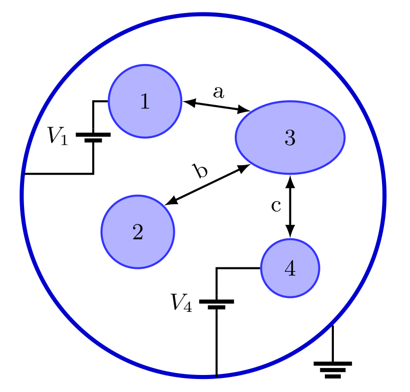
We consider an arrangement of ideal conductors characterized by their total charge and electrostatic potential , where the latter are measured with respect to some reference or ‘ground’ (see Figure 1). Basic electrostatic theory shows that the charges and potentials are related by the linear relation:
| (1) |
where and are column vectors containing the charges and voltages, and the symmetric matrix (known as the Maxwell capacitance matrix) encodes the mutual and self capacitances of the conductors. These capacitances depend on the shape, size, and relative position and orientation of the conductors. The electrostatic energy contained in such a system is given by the quadratic form:
| (2) |
Some of the conductors can have their potential fixed by voltage sources, and in that case we say that the circuit is open. We will refer to conductors with fixed potentials as regulated conductors, and to the rest as free conductors. Thus, we have , where is the number of free conductors and the number of regulated conductors. The vector will be split into vectors and containing the charges of the free and regulated conductors, respectively. If the circuit is open, then the degrees of freedom of the system are reduced. This can be seen from Eq. (1), since fixing the potential of a conductor imposes a linear relationship between all the charges. Then, the state of the system is fully specified by the charges of all the free conductors.
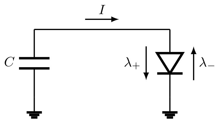
We also consider two-terminal devices or channels that allow the transport of elementary charges of value between pairs of conductors, forming a network or circuit. Each of these channels is modeled as a bi-directional Poisson process (BPP). This choice offers some generality while keeping the formalism concrete and simple and, as mentioned before, allows to describe relevant devices like tunnel junctions wasshuber2012 ; koski2013 , diodes wyatt1997 , MOS transistors in subthreshold operation sarpeshkar1993 ; wang2006 , and other devices like nanoscale vacuum channel transistors han2012 . The common feature of all these devices is that they display shot-noise (i.e., the current noise spectral density is proportional to the average current for large biases scholten2006 , see section III.1). This is also a limitation of the BPP modeling choice, since it does not allow to properly describe regular resistors or source-drain conduction in MOS transistors operating in saturation mode, where the current noise spectral density is approximately independent of the average current (as for Johnson-Nyquist noise) scholten2006 . However this is not a serious limitation, especially if we are interested in the regime of ultralow energy consumption, where the subthreshold and unsaturated operation of MOS transistors is optimal wang2006 .
Let index the two-terminal devices present in the circuit. Then, given a device connecting conductor and , we associate to it two basic Poisson processes: a ‘forward’ one in which an elementary charge is transported from conductor to conductor , and the ‘reverse’ one in which a charge is transported in the opposite direction, with respective rates and . The forward direction is of course chosen arbitrarily. Note that the rates depend explicitly on the full state of the system, which allows to model externally controlled conduction channels. Thus, in a transition the state of the system changes as:
| (3) |
where is the value of the elementary charge involved in all the possible transitions and . The vector encodes to which conductors the device is connected and what is the change in their number of charges during the transitions. If a device is connected between one of the free conductors, , and one with fixed voltage, the corresponding vector is given by:
| (4) |
where the forward direction was chosen as the one leaving the conductor with fixed potential.
One can imagine more complex devices that involve three or more conductors in an irreducible way, for example by taking one charge from conductor , one from , and transporting them to conductor . This kind of devices can also be treated with the formalism we develop here, although most discussions will be focused on two-terminal devices (that however might be controlled externally).
II.1 Reduced incidence matrix, cycles and conservation laws
The vectors can be grouped in an reduced incidence matrix:
| (5) |
This matrix is analogous to the stoichiometric matrix in chemical reaction networks polettini2014 ; rao2018 111A given circuit with two-terminal devices can be mapped to a chemical reaction network by mapping conductors to chemical species and devices to chemical reactions . This mapping only concerns the structure of the circuit and network, not the dynamics or thermodynamics.. For closed circuits it coincides with the full incidence matrix of the directed graph obtained by mapping conductors to nodes and two-terminal devices as directed edges (with the direction given by the forward one). The reduced incidence matrix for an open circuit is obtained from the one of the closed circuit by eliminating the rows corresponding to regulated conductors.
The right null eigenvectors of define cycles, i.e., sequences of transitions that leave the circuit state invariant:
| (6) |
The elements of the vectors can always be chosen to be ,, or . The number of independent cycles is . The left null eigenvectors of correspond to conservation laws, since if
| (7) |
then the quantities
| (8) |
will not change under any transition, i.e., they are determined by the initial state of the circuit. The elements of can always be considered to be or . For each connected component of the full circuit in which no conductor is regulated, we have a conserved quantity that is just the total charge of the conductors in that component. In fact, these are the only conserved quantities. Thus, the number of independent conservation laws, , equals the number of closed connected components of the circuit.
Whenever a closed circuit is opened by connecting one of its conductors to a voltage source (see Figure 1), we might either break a conservation law or create a new cycle. This can be seen in the following way. The rank-nullity theorem applied to the matrix can be expressed as:
| (9) |
This is valid for closed as well as for open circuits. Let us assume however that in the previous equation , and correspond to the matrix of the circuit in which all the voltage sources are disconnected. Then we connect voltage sources, and thus the number of conductors involved in the new matrix is now . Applying the rank-nullity theorem to we obtain:
| (10) |
Subtracting the previous two equations we see that:
| (11) |
Thus, the number of voltage sources connected to the circuit equals the number of broken conservation laws, , plus the number of emergent cycles, . This is easily understood: if a previously closed component of the circuit is connected to a voltage source, its total charge ceases to be a conserved quantity. However, if we further connect another voltage source to another conductor of the same component, then a new cycle is created (the one in which a charge is injected by one source, transported through the component, and removed by the second source).
II.2 Stochastic and deterministic dynamics
At any given time the state of the circuit is described by a probability distribution over the state space. It evolves according to the master equation:
| (12) |
where the probability currents are defined as:
| (13) |
They are simply the probability per unit time to observe a transition in state . The summation in Eq. (12) is over positive and negative values of , i.e., it is over transitions and not over devices. The set of currents can be considered the components of a vector function of the state, that we denote . We define the following operator over those functions:
| (14) |
Then, is the net probability current arriving at state corresponding to transitions , and the master equation reads:
| (15) |
Note that the change in a scalar quantity in a transition can also be expressed by trivially extending the operator to these functions:
| (16) |
The dynamical description based on the master equation in Eq. (12) is valid for timescales which are large compared to the time taken by each transition or conduction event, that here are considered to be instantaneous. This dynamics can be compared to the deterministic dynamics obtained by usual methods in circuit theory chua1987 . In those deterministic descriptions, the charges are considered to be continuous variables, and the charge vector evolves according to the following differential equation:
| (17) |
where is the electric current associated to device . The previous equation is closed by providing the I-V curve characterization of all the devices, and by Eq. (1) relating voltages and charges. For example, the current through a two-terminal device connected from conductor to conductor is considered to be a function of the voltage drop (see Section III.1). Then, can be expressed in terms of by inverting Eq. (1). The relation between the deterministic and stochastic descriptions is non-trivial and will be examined in the particular example of the CMOS inverter in section VII.1.
II.3 Equilibrium states and detailed balance
An equilibrium state of the circuit is defined as one in which the global detailed balance condition holds:
| (18) |
By Eq. (15), if an equilibrium state exists it is also a stationary one. In general no equilibrium state exists. However, for closed and isothermal circuits consistency with equilibrium thermodynamics demands the following Gibbs state to be an equilibrium one:
| (19) |
where if and otherwise, is the initial state of the circuit, and runs over a set of independent conservation laws. The partition function is such that is normalized and thus depends on the inverse temperature and the quantities . More general equilibrium states can be obtained by mixing Gibbs distributions like Eq. (19) according to a distribution on the initial state.
The demand that must be an equilibrium state when the circuit is closed and isothermal imposes minimal conditions on the transition rates . These are the local detailed balance (LDB) conditions which for closed circuits and isothermal settings are:
| (20) |
for each . They can also be written as:
| (21) |
where is a vector function of the state with components , and the function is applied element-wise. Thus, the rates characterizing a given two-terminal device must fulfill the constraints imposed by Eq. (20). We now generalize the LDB conditions to open circuits and non-isothermal settings.
II.4 Energy difference and local detailed balance
We consider an open circuit in which some conductors have the potential fixed by voltage sources. In the same way we did with the charges, the vector is split into vectors and , containing the voltages of the free and regulated conductors, respectively. We can then express the relation of Eq. (1) between all the charges and voltages as:
| (22) |
where is the capacitance matrix of the regulated conductors, is the capacitance matrix of the free conductors, and is the matrix with the mutual capacitances between conductors of the two groups. The previous equation can be rewritten as:
| (23) |
from where it is clear that, given the potentials , the charges are enough to determine the rest of the variables, as discussed before. The total electrostatic energy is then:
| (24) |
We are interested in computing how the total energy of the system (conductors plus sources) changes in a transition . From the previous equation we see that the change in electrostatic energy is
| (25) |
which is independent of the voltages . In addition to this, we need to consider the change in the energy stored in the voltage sources. This can be be computed as (minus) the work performed by them, which equals the charge transported from ground to the conductor to which each source is connected times its voltage. There are two different contributions to this work. First, the transition might directly involve one regulated conductor. If a charge arrives to the conductor fixed to a potential , it needs to be removed, and for this the source must perform an amount of work given by . Secondly, even if the transition does not involve any regulated conductor, changes in the distribution of charge among the free conductors can induce a charging of the regulated conductors. From Eq. (23) we see that the induced charge is . It follows that the total amount of work performed by the sources during transition is
| (26) |
where is a vector encoding the change in the number of charges in the regulated conductors in transition (if no regulated conductor is involved in transition , then ). Thus, the change in the energy of the system and sources can be written as:
| (27) |
where we have defined the potential
| (28) |
The first term in the right hand side of Eq. (27) is conservative, since its contribution vanishes in any cyclic sequence of transitions in the state space . The second contribution is not conservative since its contribution does not vanish in cyclic transformations: its value will depend on how the regulated conductors are involved in the cycle. Also, we note that the gradient of the potential gives the voltage of the free conductors:
| (29) |
as can be verified from Eq. (23).
The quantity is the energy required to perform the transition . By conservation of energy, it must be provided by the environment of the device , which we assume to be at thermal equilibrium at temperature (this implies that the two conductors to which is connected should also be at temperature ). Therefore, is the heat associated to device during the transition, and corresponds to an entropy change in its environment equal to . Thus, the LDB condition now reads:
| (30) |
for each , where . Equivalently,
| (31) |
For closed and isothermal settings this condition reduces to Eq. (20).
II.5 Infinite vs finite state spaces
Certain types of circuits, in particular single-electron devices, are such that the number of charges in a given conductor can only take few distinct values. They can therefore be described by truncating their infinite state space to the finite set of states relevant for the dynamics. This will not compromise thermodynamic consistency. Such approaches can also be used to model single-electron traps which can be useful to model random telegraphic and noise, as we will discuss in section III.2.3.
For many other circuits, such truncation to a small state space is not possible. Infinite state spaces are indeed a crucial ingredient of devices displaying a macroscopic limit. This is the case of CMOS circuits for instance, where as the typical size of the transistors is increased, the number of electrons in each conductor becomes very large. In this case the stochastic dynamics gives rise to a deterministic non-linear dynamics (described by Eq. (17)), which enables the emergence of complex phenomena such as bistabilities, oscillations, and chaos. Studying fluctuations can become very expensive numerically and many techniques suitable for finite state space (e.g spectral methods) will not be applicable anymore. Also, common approximation techniques such as the second order truncation of the Kramers-Moyal expansion of Eq. (12) leading to Fokker-Planck or Langevin equations, are known to produce incorrect results hanggi1988 ; horowitz2015 . One must therefore resort to more elaborate methods such as path integrals and large deviations techniques doi1976 ; lefevre2007 ; touchette2009 . Such methods have been used to study stochastic chemical reaction networks lazarescu2019 where similar problems are encountered horowitz2015 .
III Models for Devices
III.1 I-V curve characterization
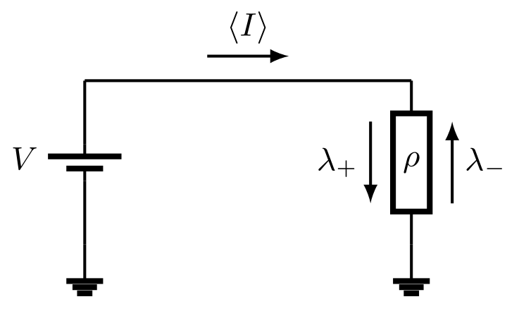
Two-terminal devices are usually characterized by measuring how the average electric current through them depends on the applied voltage across their terminals, as in Figure 2. Modeling a device as a BPP with rates and , and applying the LDB condition of Eq. (30) to this simple case, we obtain:
| (32) |
The net amount of charge going through the device in the forward direction between time and is:
| (33) |
where are independent Poisson processes with rates . The average current is then:
| (34) |
Thus, the BPP modeling assumption and the LDB condition allows to determine the rates from the measurement of the I-V curve alone, via Eqs. (32) and (34). In turn, from these rates we can compute any statistical moment of the electric current . Therefore the full statistics of the process is completely determined by just the mean value . In particular, the second central moment is wyatt1997 ; wyatt1999 :
| (35) |
which at variance with the first moment depends explicitly on the integration time . This integration time is related via the Nyquist-Shannon sampling theorem to the frequency bandwidth of the measurement. Thus, in the limit of large bias () we obtain the usual expression for shot noise:
| (36) |
Then, in this context, shot noise appears as a direct consequence of the BPP assumption and of the LDB condition. For this reason, the fluctuations in circuits with elements that do not display shot noise cannot be faithfully described with this formalism. In the opposite limit where thermal effects dominate (), we recover the usual expression for Johnson-Nyquist noise sarpeshkar1993 ; landauer1993 .
III.2 Specific devices
III.2.1 Tunnel junctions
A tunnel junction is the simplest kind of device and the one for which the BPP model is more natural (in some regimes of operation) wasshuber2012 . Here we will consider a tunnel junction consisting of a sufficiently small gap between two metallic islands at room temperature, such that electrons can tunnel through the gap. It typically displays an Ohmic I-V curve fulton1987 ; wasshuber2012 : , where the tunnel junction resistance can be computed from the specific properties of the metal conductors and the transmission coefficient of the junction. Using Eqs. (32) and (34) we obtain the rates:
| (37) |
These expressions are well defined for any positive or negative value of the elementary charge , and if it changes sign then the roles and are just inverted. Many other different kinds of tunnel junctions exist, which can display strongly non-linear I-V curves depending on the spectral densities of the materials constituting the junction (see wasshuber2012 for a quick review).
III.2.2 Diodes
The characteristic curve of a p-n junction diode is often modeled via the ideal Shockley diode equation shockley1949 :
| (38) |
where in this case is the positive electron charge and is the reversed bias saturation current. Then the Poisson rates are given by:
| (39) |
where we have defined the thermal voltage
| (40) |
III.2.3 MOS transistors in weak inversion
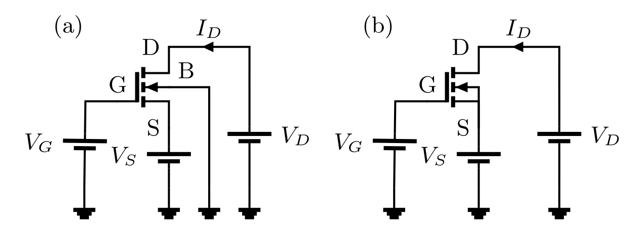
MOS transistors are ubiquitous devices underlying most of modern digital and analog electronics. An enhancement-mode nMOS transistor like the one depicted in Figure 3 has two typical modes of operation: (i) a saturation mode, and (ii) a subthreshold or weak inversion mode (see tsividis2011 for a rigorous discussion of all the modes of operation). In the saturation mode the transistor essentially behaves like a switch, allowing conduction between source (S) and drain (D) if the gate (G) voltage is above a certain threshold (see Figure 3-(a)). If then source-drain conduction is suppressed. However, whenever some small leakage current will still flow, and its magnitude will greatly depend on how far is below . This is the subthreshold mode of operation, on which we focus in the following. To describe this mode, we consider the Enz-Krummenacher-Vittoz model of the MOS transistor as developed in enz2006 . According to this model, the average drain current can be naturally split into forward and reverse components given by:
| (41) |
where the voltages and the current are defined as in Figure 3-(a). This model of the MOS transistor in subthreshold operation involves three parameters characterizing the device: the threshold voltage , the ‘specific’ current and the ‘slope factor’ . All these parameters can be determined from a microscopic description of the device as explained in enz2006 . The total average drain current is then:
| (42) |
In the previous expression the symmetry of the device is preserved, since we see that the current is inverted if we interchange the roles of drain and source. For the more common three-terminal configuration of Figure 3-(b), the symmetry is broken and the current is given by:
| (43) |
The voltage bias driving this current is , which plays the role of in the I-V curve characterization. Using this last expression we obtain the following Poisson rates:
| (44) |
In principle this model is accurate only for .
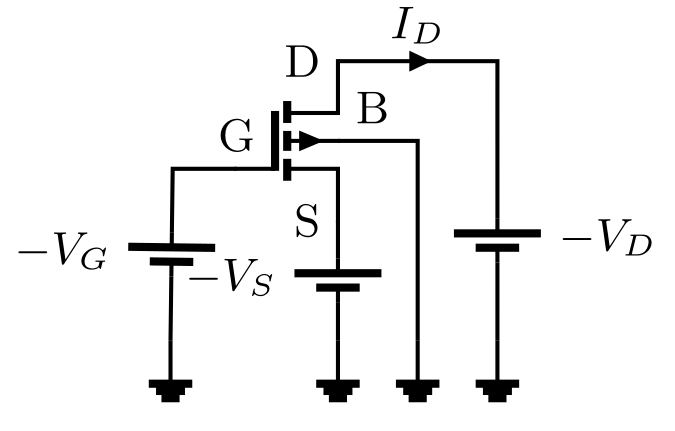
In a pMOS transistor conduction between drain and source is increasingly allowed as the gate voltage becomes negative with respect to the body, contrarily to the nMOS transistor. However, all the expressions presented for the nMOS transistor are still valid for pMOS transistors provided that the sign of the currents and voltages are reversed, as Figure 4 indicates.
In general treatments, the noise in MOS transistors is modeled by integrating infinitesimal Johnson-Nyquist sources along the drain-source channel enz2006 ; tsividis2011 . However, for the subthreshold or weak-inversion mode in which we are interested, the results obtained in that way are fully compatible with those obtained from a simple BPP model as considered here sarpeshkar1993 . This is not the case for other modes of operation. We note that this discussion only concerns the noise associated with the transport processes. Other kinds of noise associated with the presence of defects and charge traps ( and/or random telegraphic noise) play a role in MOS transistors kirton1989 ; Chen2015Dec ; VanBrandt2019 , and are relevant at low frequency. Random telegraphic noise can nonetheless be modeled within the framework using individual charge traps, as briefly mentioned in section II.4. can be modeled as well as it can be generated by an ensemble of random telegraphic sources paladino2014 .
IV Charging effects
The previously discussed I-V characterization of two-terminal devices allows to determine the Poisson rates for a given device in situations where the voltage across the device is kept fixed. In actual circuits this voltage will of course depend on the full state of the circuit, in accordance with the relation of Eq. (1). Thus, the Poisson rates will be functions of the full state. However, naive constructions of the functions , based on the I-V characterization and Eq. (1), fail to fulfill the LDB conditions. As a consequence, they would lead to unphysical non-thermal stationary states for closed and isothermal circuits. To discuss and illustrate this situation, we revisit the well known ‘Brillouin’s paradox’ brillouin1950 . Based on the analysis of this problem we derive a procedure to construct the rates for arbitrary devices and circuits in such a way that the LDB conditions are always respected.
IV.1 Brillouin Paradox
We consider the circuit of Figure 5: a closed and isothermal circuit consisting of a diode and a capacitor connected in parallel. At any given time the voltage across the diode is equal to the capacitor voltage , where is the total charge in the upper capacitor plate. Then, to construct the Poisson rates we might consider the following procedure: to obtain the rate for a transition , we evaluate the fixed-voltage rates of Eqs. (39) at the voltage preceding the transition (we refer to this as a ‘naive causality’ assumption). In this way, we have:
| (45) |
However, these rates do not fulfill the LDB condition of Eq. (20), that for this simple case reads:
| (46) |
where is the energy of the circuit. As a consequence, the stationary distribution corresponding to the transition rates is:
| (47) |
which deviates from the correct Gibbs equilibrium by a factor . Since this factor is an uneven function of the charge, it follows that the stationary mean value of the charge in the capacitor is strictly below . If this were the case, the capacitor could be disconnected from the diode and employed as a source of energy, and this process could in principle be repeated indefinitely. This apparent violation of the second law is essentially the Brillouin paradox, and can be considered the electronic analogue of a Brownian ratchet.
A way to solve this problem is to notice that the LDB condition of Eq. (46) would be fulfilled if the fixed-voltage rates were evaluated not at the voltage before each transition, but at the average of the voltage before and after the transition. Using this midpoint rule we obtain the rates wyatt1997 ; wyatt1999 :
| (48) |
which lead to the correct Gibbs equilibrium. Later we will show that the midpoint rule is valid in general. This means that it can be applied to the fixed-voltage rates of an arbitrary device to obtain thermodynamically consistent transition rates when this device is embedded in an arbitrary circuit. Although this rule seems to be at odds with the notion of causality, it is actually not: the probability of a transition naturally depends on the final state as well as on the initial one. For the naive notion of causality to be preserved one should modify the characteristic I-V curve of the device in question in a way that is context dependent. This in turn challenges the idea of modularity, i.e., the notion that the behavior of a device is not influenced by its environment and therefore can be plugged in different circuits without modifying its description, which is a basic assumption in the usual modeling of complex electronic circuits at the deterministic level. However, modifications to the characteristic curve of a device due to charging effects in its environment are well known in the study of single electron devices, where the most explicit example is known as the Coulomb blockade effect averin1986 ; fulton1987 ; devoret1990 ; ali1994 ; wasshuber2012 ; grabert2013 ; bagrets2003 . In the following we illustrate the charging effects in the context of the Brillouin paradox.
IV.2 Charging effects in the I-V curve
Let be the average current for a given value of the capacitor voltage in the example of Figure 5. According to the correct rates of Eqs. (48), it reads:
| (49) |
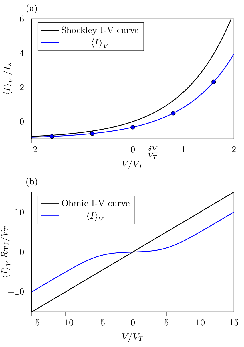
which match the characteristic I-V function of Eq. (38) evaluated at a voltage shifted by . At the same time, the standard deviation of the voltage is . Then, charging effects are relevant whenever is comparable to and . Consequently, in order to observe or employ these effects, as done for example in single electron transistors, one either needs to work with nanoscopic circuits (in order to achieve low values of C) or at low temperatures (usually a combination of both). The characteristic curves of Eqs. (38) and (49) are compared in Figure 6-(a). We note that, counter to intuition, the mean value does not vanish for . This seems to indicate that an initially empty capacitor would charge up when connected to the diode. However, in accordance to the second law, this anomaly is effectively neutralized by thermal fluctuations. This can be verified by computing the mean value of the current for the Gibbs equilibrium distribution :
| (50) |
Also, for we have , and thus it seems that for those values of the device is actually delivering power. However this is not the case since the actual voltage can only take the discrete values , with integer, as indicated with dots in Figure 6-(a). Finally, we note that if we take the limit while fixing the voltage , which correspond to a model of a perfect voltage source, charging effects disappear (we go back to the picture of Figure 2).
IV.3 General case
Comparing Eqs (32) and (30) we see that if in the fixed-voltage rates is replaced by , then the resulting state dependent rates will automatically satisfy the LDB condition (recall the definition of in Eq. (27) and note that it satisfies ). Explicitly, we should consider (for ):
| (51) |
In turn, if device is connected to conductors and (with as the forward direction) then we have:
| (52) |
where is the average of the voltage difference before and after the transition . This justifies the midpoint rule mentioned above and can be easily verified from the relation of Eq. (23) and the definition of in Eq. (28).
Particular care should be taken for the case of the MOS transistor (or in general with three-terminal devices that can be considered as externally controlled two-terminal devices). In this case the fixed-voltage transition rates for the source-drain conduction do not depend only on the voltage difference between those terminals, but also on the ‘control’ voltage . Generalizing the rates of Eq. (44) we can write:
| (53) |
where the functions and are such that the following condition is satisfied:
| (54) |
To construct state dependent rates satisfying the LDB condition of Eq. (30), we should not only replace by its average before and after the transition but also do the same with the control parameter . Explicitly:
| (55) |
An analysis similar to the one for the diode in section IV.2 also holds for more general circuits, including CMOS circuits. If is the typical capacitance at a given node of a circuit, the standard deviation of the voltage fluctuations at that node can be estimated by its equilibrium value , where we have defined the elementary voltage which represents the voltage change associated to a single charge jump. Values of as low as aF can be attained in modern CMOS fabrication processes zheng2016 , that at room temperature lead to elementary voltages as high as , and thus . Then, we see that in modern subthreshold or near threshold applications it is not possible to neglect charging effects nor thermal fluctuations if the operating voltages are comparable to the thermal voltage . This in turn opens new possibilities that are explored in the example of section VII.2.
IV.4 Charging effects and non-linearity
Circuits containing devices with non-linear I-V curves are qualitatively different from circuits in which all devices are linear. For example, in linear RLC networks (where the degrees of freedom are continuous and the stochastic dynamics is described by a Fokker-Planck equation), the dynamics of the mean or expected values of voltages and currents is decoupled from the dynamics of higher order moments, and therefore it matches the deterministic dynamics freitas2019 . This is not anymore the case if some non-linear element is present. However, in the kind of discrete models we are considering here, charging effects can induce non-linear behaviors even if the characteristic I-V curves of all the devices in the circuit are linear, as is the case with tunnel junctions averin1986 ; devoret1990 ; ali1994 . This is illustrated in Figure 6-(b), that was obtained in the same way as Figure 6-(a) for the diode. These induced non-linearities are a resource that is exploited in the construction of single electron transistors and logic gates only consisting of small conductive islands and tunnel junctions between them wasshuber2012 . However, in the macroscopic limit in which each conductor has many excess charges, or for high temperatures, the non-linear effects are washed out. Consequently, in those regimes, the expected values of voltages and currents in such circuits will obey closed and linear equations of motion that will match the ones obtained from the deterministic description of Eq. (17). The question about the relation between the stochastic and deterministic descriptions in general circuits is non-trivial, and will not be addressed here in full generality. It will be analyzed for the particular example of the CMOS inverter in Section VII.1. A general treatment will be considered elsewhere, based on Large Deviations Theory lazarescu2019 ; cossetto2020 ; freitas2021 .
V Stochastic thermodynamics
So far we have established the general stochastic description of electronic circuits and we have shown how to construct the transition rates corresponding to different devices in a way that is thermodynamically consistent. In the following we explore the general properties of this kind of models. We start by analyzing the energy balance and the entropy production, i.e., we establish the first and second laws. For this we first define the production of heat in each device and its relation to the electric current.
V.1 Electrical currents and heat dissipation
Let us consider the following pair of transitions, which are the inverse of each other:
| (56) |
The average electric current corresponding to this pair of transitions is:
| (57) |
And then the net average electric current corresponding to device is:
| (58) |
In a similar way, the average rate at which heat is provided by the environment of device corresponding to that pair of transitions is:
| (59) |
where is the change in energy of the system during transition and is given by Eq. (27). Note that, as is usual in stochastic thermodynamics but contrary to what is normally done in electronics, heat is defined as positive when it increases the energy of the system. Recalling Eq. (52), if device is connected to conductors and , we can write:
| (60) |
This is the stochastic version of the usual formula for Joule heating. Note that it is only valid at the level of transitions, and that the average voltage difference is involved. The net heat rate associated to device is:
| (61) |
where we have employed Eq. (27) to substitute .
V.2 Balance of Energy
Let us consider the rate of change in the mean value of the potential :
| (62) |
The explicit time dependence of accounts for possible external controls of the parameters entering its definition, like the elements of the capacitance matrix or the voltages of the regulated conductors. Thus, the contribution is interpreted as the rate of work done by this external control:
| (63) |
Then, employing the master equation of Eq. (12), we can write:
| (64) |
In the second and third lines of this equation we used the symmetry . Note that at variance with the first line, the sums in the last line only involve positive values of and therefore can be considered as sums over devices. According to Section II.4, the quantities
| (65) |
are the average rates of work performed by the voltage sources corresponding to device . In this way we obtain the following energy balance for a general circuit:
| (66) |
V.3 Entropy production
To the probability distribution we assign the Shannon entropy:
| (67) |
which, as the notation suggests, can be considered the average of the state dependent entropy . Its time derivative is
| (68) |
As usual, this rate of entropy change can be split into two components:
| (69) | ||||
Using the LDB condition in Eq. (31) the second term can be related to the average entropy production in the environment:
| (70) |
Thus, combining the last two equations we obtain the following expression for the total average irreversible entropy production:
| (71) |
which is explicitly positive. This constitutes a proof of the second law of thermodynamics in this context. We see that the entropy production vanishes if and only if , i.e., if the state is an equilibrium one (see Eq. (18)). The fact that corresponds to the familiar concept of entropy production is further justified in the following.
V.3.1 Isothermal conditions
If the temperature of all the devices is the same then we can split the total entropy production into a potential term and a work term. To see this we combine Eqs. (70) and (66) and write:
| (72) |
where is the common temperature of all devices. Then, we obtain:
| (73) |
where we have defined the average free energy as:
| (74) |
Thus, the temperature times the total entropy production rate was expressed as a change in a thermodynamic potential plus the total work performed on the system. Integrating Eq. (73), and using the fact that , we recover the usual statement of the second law: the amount of work that can be extracted from the system during an arbitrary transformation is limited by minus the free energy difference.
V.4 Equilibrium states
Due to the LDB conditions, for time-independent, closed and isothermal systems there is always an equilibrium state satisfying Eq. (18), and it is given by Eq. (19). However, equilibrium states could also exists under more general conditions. For example, if an isothermal and closed circuit is opened by connecting some or all connected components to a voltage source (in such a way that there is only one voltage source connected to each component), then there also exists an equilibrium state, in which no currents flow. To see this, we notice that in such a case also the second term in Eq. (27) is conservative. In fact, we can write:
| (75) |
where indexes the regulated conductors, is the voltage of conductor , and
| (76) |
is the total charge of the free conductors in the connected component to which conductor belongs. Here the vectors can be constructed as the reduction to the space of free conductors of the left eigenvectors of the incidence matrix of the full circuit, including the regulated conductors. We see then that in this case the energy change during a transition can be expressed as the change in a state function :
| (77) |
with
| (78) |
Thus, it follows that for isothermal conditions there exists an equilibrium state satisfying the global detailed balance conditions of Eq. (18). It is given by:
| (79) |
where the index runs over the closed connected components of the circuit, is the total charge of component as defined by Eq. (8), and is the initial state. As with Eq. (19), the partition function is such that is normalized and thus depends on the conserved quantities .
V.5 Fundamental non-equilibrium forces
Based on the previous discussion, we can now split the work performed by the sources into conservative and non-conservative contributions. For this we first split the set of regulated conductors into two categories. For each of the open connected components in the full circuit we arbitrarily select one of its regulated conductors. The conductors selected in this way are indexed by . As will be clear later, the subindex stands for ‘potential’. The total number of ‘potential’ conductors can be easily seen to match the number of broken conservation laws as defined in section II.1. The rest of the regulated conductors are indexed by . In this case the subindex stands for ‘force’, and equals the number of emergent cycles. In this way, to each transition involving a regulated conductor we can assign: (i) the voltage of the regulated conductor involved in that transition, and (ii) a reference voltage , that is the voltage of the regulated conductor that was selected as ‘potential’ in the corresponding open connected component. Thus, the energy change during a transition involving a regulated conductor can be rewritten as:
| (80) | ||||
where is the total charge on the free conductors in the open connected component of conductor , as defined in Eq. (76). Thus, the heat rate of device , Eq. (61), can also be expressed as:
| (81) | ||||
where is the potential defined in Eq. (78). To each device we can assign a voltage difference . The minus sign in this definition was introduced in order to make positive whenever the reference voltage is the lowest one in each connected component, and the forward direction of device is the one leaving the regulated conductor. For a “internal” device not connected to any regulated conductor, or for a device connected to a regulated conductor at the reference voltage, . Then, we see that at most voltage differences can be different from zero. They are considered elements of a set of fundamental voltage differences, or non-equilibrium forces. Therefore, the total heat rate can be written as:
| (82) |
where is one of the fundamental non-equilibrium forces or voltage differences, and its associated electric current.
V.6 Minimal decomposition of the isothermal entropy production
For isothermal settings, the entropy production can be decomposed in a similar way as in section V.3.1, this time in terms of the grand potential
| (83) |
and the fundamental forces . To see this, we start by computing the change in the potential :
| (84) |
As before, we define a rate of work associated to the external control of the system:
| (85) |
Note that this rate of work only coincides with in Eq. (63) if the voltages of the regulated conductors are time independent. Now, combining the last two equations with Eq. (82) and recalling that for isothermal settings we have , we obtain:
| (86) |
that leads to the following expression for the irreversible entropy production:
| (87) |
where
| (88) |
is naturally defined as the work rate associated to the fundamental voltage difference . We see that if the system is not driven () and there are no fundamental forces , then . Also, from the fact that the capacitance matrix is positive definite, it follows that the thermodynamic potential is bounded from below. Thus, when , is a Lyapunov function that reaches a minimum at equilibrium.
V.7 Non-equilibrium Landauer principle
Let us consider a transformation between two arbitrary, possibly non-equilibrium, states and . This transformation is driven by changing in time the parameters of the circuit (for example the elements of the capacitance matrix or the properties of some of the devices), and/or by modifying the voltages of the regulated conductors. This can induce a parametric driving of the potentials and (and thus also the free energies and ), as well as a change in the non-equilibrium forces to which the system is subjected. In the following we will consider the time dependent equilibrium state , which is just the equilibrium state of Eq. (79) corresponding to the parameters of the system at time , and that will serve as a reference state. Also, given an arbitrary state (compatible with the conserved quantities ), we introduce its relative entropy with respect to the equilibrium state :
| (89) |
which in simple terms measures how much information should be provided in order to identify the state starting from . It vanishes if and only if , and is always positive otherwise. By employing the explicit form of the equilibrium state it is easy to see that the relative entropy can be computed as a difference between average free energies:
| (90) |
where is the non-equilibrium free energy and is the equilibrium one. Using Eq. (90), we can rewrite Eq. (87) as:
| (91) |
Integrating this relation over time and using that we obtain
| (92) |
Thus, the previous expression provides a bound for the amount of work necessary to perform (or that can be extracted during) a transformation between arbitrary states. Importantly, this bound explicitly takes into account the ‘information content’ of the initial and final states with respect to the ‘uninformative’ equilibrium, and it can be considered a general version of the Landauer principle esposito2011 . The connection to the notion of logical or computational information is achieved by splitting the state space into different logical subspaces. This was done in sagawa2014 , where a bound equivalent to Eq. (92) was derived.
The Landauer principle is commonly discussed in terms of physical memories that represent logical values as quasiequilibrium metastable states, of which the proper thermal equilibrium is a mixture sagawa2012 ; sagawa2014 ; parrondo2015 ; riechers2018 . However, it is important to notice that in some relevant kinds of electronic memories logical values are represented by non-equilibrium steady states (NESSs) that continuously produce entropy (for example, SRAM cells, or the probabilistic bit discussed in section VII.2). Although the Landauer principle can anyway be applied to those cases, the bound obtained from the right hand side of Eq. (92) does not take into account that continuous entropy production (or “housekeeping heat” speck2005 ), or any other additional dissipation due to restrictions on the control parameters of the system kolchinsky2020constraints . Refinements of the Landauer principle based on lower bounds for the entropy production in non-adiabatic transformations can be obtained schmiedl2007 ; sivak2012 ; diana2013 ; zulkowski2014 ; proesmans2020 ; nicholson2020 , but to the best of our knowledge the physics of computation with NESSs remains poorly explored.
VI Stochastic trajectories and fluctuation theorems
In the previous sections we have studied the average or expected values of relevant quantities like the energy, entropy or work. In this section we turn to a lower level description based on single trajectories in the state space of the circuit, that will allow us to formulate different fluctuation theorems. We closely follow the treatment in rao2018 for chemical reaction networks and of rao2018detailed for general Markov chains. Here we only present the main results and the necessary definitions. Additional details about the derivations can be found in the supplementary material.
We define a trajectory as a particular realization of the stochastic dynamics, from some initial time up to time . Thus, a particular trajectory is fully characterized by its initial state , the set of transitions that took place up to time , and the times at which they occurred. The index takes the values , where is the number of transitions up to time . All this information can be encoded in the trajectory probability current:
| (93) |
where is the state immediately before instant . Different trajectories will occur with different probabilities. If the evolution of the system is well described by the master equation of Eq. (12), then the probability density of observing trajectory given that the initial state is satisfies:
| (94) |
where we have defined . The factors in the first product account for the probabilities of not having any transition during the periods , while the factors in the second product are proportional to the probabilities of each of the jumps to take place. If we average Eq. (93) over all trajectories then we recover the probability currents of Eq. (13).
The average quantities defined in the previous sections can be easily extended to individual trajectories. For example, the instantaneous electric current and power of device are:
| (95) |
and
| (96) |
These are just the stochastic versions of the average quantities in Eqs. (81) and (57), respectively, and are obtained by simply replacing the average current vector by the stochastic one, , which is a vector function with components . is one of the fundamental non-equilibrium forces defined in Section V.5.
The net change of a state function during a trajectory can be expressed in terms of the currents in the following way:
| (97) |
Applying this expression to the potential defined in Eq. (78) we can arrive to the following energy balance for a given trajectory:
| (98) |
where
| (99) |
is the external driving work performed during the trajectory,
| (100) |
is the heat corresponding to device , and
| (101) |
is the work performed by the fundamental non-equilibrium force ( is its associated electric current).
VI.1 Stochastic entropy and the integral fluctuation theorem
As mentioned before, it is possible to define the entropy of a given state during a trajectory in the following way seifert2005 :
| (102) |
where is the solution of the master equation in Eq. (12) for a given initial distribution . The entropy flow, i.e., the production of entropy in the environment during a given trajectory is
| (103) |
Then, the total entropy production during the trajectory is:
| (104) |
It can be verified that the time derivatives of the averages and over all trajectories match the entropy production rates and defined in Eqs. (70) and (71). Unlike its average , the entropy production of a given trajectory is not always positive. However, the fluctuations of are bound to satisfy a general integral fluctuation theorem (IFT). This fundamental result is expressed as the following equality:
| (105) |
where the average is taken over all trajectories . In simple terms, this equality states that positive values of the full entropy production are more probable than negative ones. Accordingly, from this result and Jensen’s inequality the usual statement of the second law follows: . Eq. (105) is valid for transient or steady state dynamics, in autonomous or time-dependent circuits.
VI.2 Detailed fluctuation theorems
Equation (105) is only one of several fluctuation theorems. Under certain conditions, other quantities different from the full entropy production satisfy more stringent constraints. For example, in isothermal settings where for all , it is possible to obtain the following detailed fluctuation theorem (DFT):
| (106) |
In this expression, is the probability to observe the values of work for each of the fundamental forces and of for the driving work during a forward protocol. This protocol consists on the initialization of the system state at according to the equilibrium state of Eq. (79), and its subsequent evolution according to the transition rates up to time (the explicit dependence of the rates on takes into account a possible external manipulation of the circuit parameters, leading to an inhomogeneous time evolution). Analogously, the quantity is the probability to observe the work values and during the corresponding backward protocol, in which the system is initialized in a state drawn from the equilibrium distribution of Eq. (79) (this time corresponding to the circuit parameters at time ), and evolves according to the rates .
The previous result holds for arbitrary times , under the condition that the initial state is an equilibrium one. A complementary relation can be obtained, which is only valid asymptotically (that is, for long times), but irrespective of the initial distribution (under the additional assumption that the circuit state is bounded to a finite region of the state space). It reads:
| (107) |
where we have defined the average work rates and . Note that in the case in which the voltage differences are constant we have , where are the average associated currents during the trajectory, and therefore Eq. (107) can be easily expressed in terms of the probabilities . If there is no external driving of the circuit parameters, then .
The fluctuation theorems in Eqs. (106) and (107) express fundamental symmetries of energy exchange processes. For example, the novel thermodynamic uncertainty relations timpanaro2019 , or the usual Onsager relations (as well as their non-linear extension gu2020 ) can be recovered from them. For completeness, a general proof of these and others fluctuation theorems is given in the supplementary material.
VII Applications
VII.1 The CMOS inverter
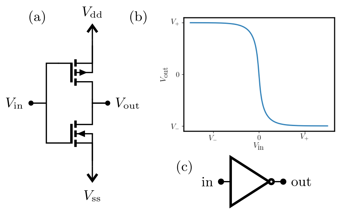
The inverter or NOT gate is the most elementary logic gate. It has a single logical input, which is negated in its only output. A diagram of a possible implementation of this gate with MOS transistors is shown in Figure 7-(a). It is composed by one pMOS (top) and one nMOS (bottom) transistors, with common drain and gate terminals. The device is powered by applying a voltage difference between source terminals. When the voltage in the input is , conduction in the nMOS transistor is suppressed while it is enhanced in the pMOS transistor, and therefore the output voltage rapidly approaches . The situation is reversed for , as shown in Figure 7-(b).
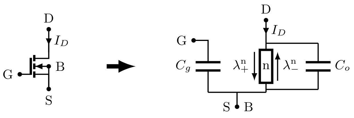
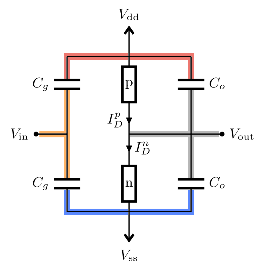
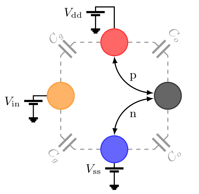

Now we explain how to build a stochastic model of the inverter within our formalism. The first step is to model the MOS transistor as an externally controlled conduction channel, with associated capacitances. For example, the nMOS transistor at the bottom of the diagram of Figure 7-(a) can be represented as in Figure 8. There, the transistor is represented as an externally controlled conduction channel between source and drain. The Poisson rates associated to that channel are constructed as explained in section IV.3, and will depend on the gate to source voltage as well as on the drain to source voltage. The gate-body interface is modeled as a capacitor of capacitance , and another capacitor takes into account the output capacitance of the transistor. Using this mapping, we can model the full inverter with the diagram of Figure 9. In turn, this diagram corresponds to a set of four conductors, in which 3 of them are regulated by voltage sources, as shown in Figure 10. The relation between the charges and voltages in this system is given by
| (108) |
where is the charge of the only free conductor (the output of the gate), and to which we will refer simply as in the following. By comparison with Eq. (22) we can extract the blocks , and of the capacitance matrix (separated by lines in the previous expression). Using that and Eq. (24) we obtain the internal energy of the circuit as a function of the only degree of freedom :
| (109) |
with . In the same way, from Eq. (28), we can obtain the potential
| (110) |
and by taking its gradient we obtain the output voltage as a function of :
| (111) |
Also, by selecting as the reference voltage to construct the potential (Eq. (78)), we find
| (112) |
and that as defined above is the only non-equilibrium force (with , the current through the pMOS transistor, as the associated current).
According to Eq. (98), the energy balance for this circuit at the trajectory level is:
| (113) |
where and are the heat currents associated to each of the transistors. The irreversible entropy production is given by Eq. (87) and for this case reads:
| (114) |
where is the temperature of both transistors and (we assume time independent voltages, so the driving contribution of Eq. (85) is not present). As can be seen from the two previous equations, for steady state conditions (), the entropy production reduces to the entropy flow and we recover the usual expression:
| (115) |
We now build the transition rates associated to both transistors according to the procedure of Section IV.3. We begin with the nMOS transistor. The voltage difference between drain and source is , and thus its average during the transition , with rates , is . For the pMOS transistor, the voltage difference between source and drain is (recall that for pMOS transistors the references for voltage and currents are reversed), and its average for the same transitions, this time with rates , is . Then, via the procedure of Section IV.3 and the fixed-voltage rates of Eq. (44), we obtain the transition rates
| (116) |
for the nMOS transistor, and
| (117) |
for the pMOS. Thus, the master equation for the distribution reads:
| (118) | ||||
The master equation can be employed, for example, to find the steady state for given voltages , and . As shown in the supplementary material, this can be done analytically, and the steady state is uniquely determined by the following recurrence relation:
| (119) |
where we have defined the constants:
| (120) |
and
| (121) |
From Eq. (119) it follows that the mean value can be obtained from the positive root of
| (122) |
as . The constants and are such that:
| (123) |
where the mean value is taken on the stationary state given by Eq. (119) (see supplementary material). Thus, and quantify the fluctuations of the output charge around the mean value. They are defined so that if the stationary state was a thermal equilibrium state (as it is for ), then . The constant is a measure of how the even moments of around the mean value deviate from those corresponding to equilibrium, while is the same for the odd moments. We see then that Eq. (122) determines how the non-equilibrium fluctuations, characterized by and , affect the expected output of the gate . If we assume that the fluctuations are always compatible with thermal equilibrium (i.e., if ), then Eq. (122) reduces to what it is obtained from a deterministic analysis of the circuit (Eq. (17)). Thus, this equation constitutes an exact stochastic generalization of the deterministic results that to the best of our knowledge was not obtained before.
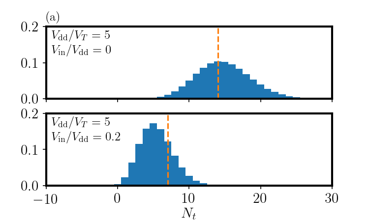
In Figure 11-(a) we show the probability distribution for the output charge for different values of the power and input voltages. When there is no voltage bias applied to the gate (), the distribution is just the equilibrium one. When a bias is applied but there is no input voltage ( and ), the distribution is stretched out and it ceases to be Gaussian. The application of a small input voltage tilts this distribution to one side, and a further increase of the input voltage generates an approximately Gaussian peak centered around the value corresponding to the deterministic solution. We see that the distribution of the output charge is in general asymmetric with respect to the deterministic value. Thus, its mean value and the deterministic one will differ. This is further evidenced in Figure 11-(b), where we plot the parameters and as a function of the input voltage. We see that the largest deviations from equilibrium occur around zero input voltage, when the two transistors are equally activated, while they rapidly decrease as one of the transistors is more activated than the other. What happens here is that for large positive (negative) the output conductor is approximately at equilibrium with the source (). Consequently, the current through the device (and therefore the entropy production), follow a similar pattern. Finally, in Figure 11-(c) we show the deviations of the actual transfer function of the inverter from the deterministic one, caused by non-equilibrium fluctuations.
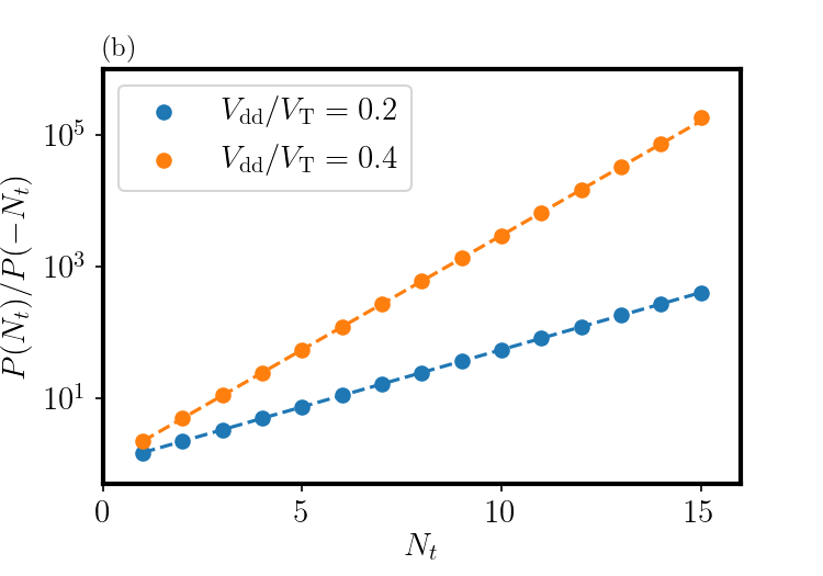
We now turn to the analysis of the current fluctuations. For this we employ the method for full counting statistics bagrets2003 ; esposito2007 , that we review in the supplementary material. This method allows to evaluate the characteristic function associated to the currents fluctuations in terms of the generator of the master equation. Then, the characteristic function can be inverted to obtain the probability distribution. We consider the number of charges that went through the pMOS transistor during a time , starting from the stationary distribution. In Figure 12-(a) we show the probability distribution of for different input voltages, with , where is the natural time scale for this problem. Also, in Figure 12-(b) we illustrate the DFT of Eq. (106), which in this case reads:
| (124) |
assuming an initial state , with given by Eq. (112).
From Figures 11-(a) and 12-(a) we see that, except when the number of charges is too low (as in the bottom panel of Figure 12-(a)), the deterministic solution matches the most probable result according to the stochastic treatment. This is analogous to what has been formally shown in the case of chemical reaction networks using large deviation theory lazarescu2019 .
These results and methods set the stage for more interesting problems, since the NOT gate is a basic primitive in electronic design in terms of which more complex devices can be built. For example, connecting the output of the gate back to its input through some conduction channel we can generate self-sustained oscillations. Connecting two NOT gates in a loop we obtain a bistable system with two metastable NESSs, which is the basis of many designs of electronic memories, and also of the next example. More complex logic gates can be modeled in the same way. We have only analyzed the stationary distribution of the inverter for a given input voltage, although in a real application the energetic cost of switching the inputs is a significant contribution to the total entropy production. This cost can be analyzed by letting the input change in time in a predefined way. Alternatively, it can also be studied in autonomous circuits (i.e., not requiring time dependent external driving) displaying bistability or limit cycles, as is done in the next section.
VII.2 A full-CMOS probabilistic bit
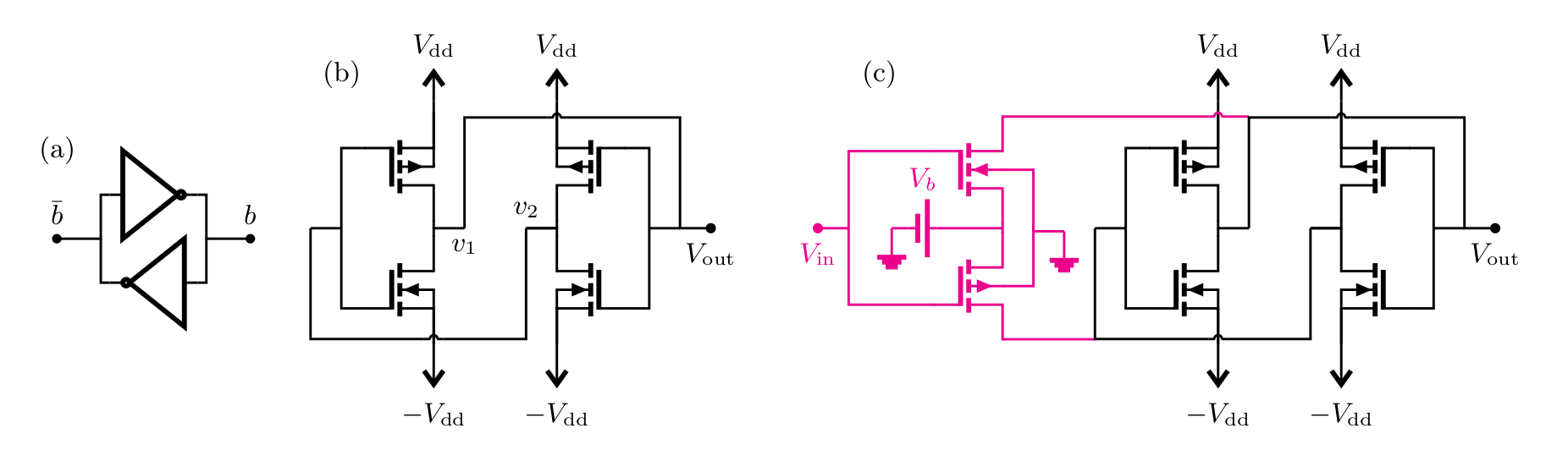
A probabilistic bit (-bit), or binary stochastic neuron, is a device with a single output that can ideally take only two values, let us say and . It outputs the value with probability , and with probability . The value of is controlled by an input . For large positive values of , , while for large negative values . In a collection of of these elementary devices, the inputs could be adjusted as a function of the instantaneous state , and in this way correlations between different -bits can be established borders2019 . For example, given a cost function , it is possible to derive functional relations such that the state occurs with probability . The function can then be chosen so that its minimum (the most probable state) encodes the solution to some problem of interest lucas2014 . Alternatively, the function can be “learned” in order for to approximate the distribution of a given data set ackley1985 .
There have been recent proposals to implement -bits with noisy electronic circuits. The most relevant employs magnetic tunnel junctions (MTJs), a technology being used for some commercial memories bhatti2017 , modified on purpose so that they are sensitive to thermal noise (by lowering the energy barrier separating the two possible states representing one bit) camsari2017 ; borders2019 . A previous proposal considers a “probabilistic switch” cheemalavagu2005 ; akgul2006 : a regular CMOS inverter which is driven by external noise at its input, so that its output fluctuates between the two possible values. The advantage of this second proposal is that it is based on CMOS circuits only (not on less common devices like MTJs). However, its main drawback is that the intrinsic noise is actually neglected, instead of being exploited as a resource. The reason is that the description of the CMOS inverter is purely deterministic, and therefore access to an external source of noise is assumed. Also, the noise is considered to be Gaussian, which as we have seen in the last section is not always the case. These limitations are of course related to the difficulty of describing intrinsic noise in non-linear electronic circuits, as discussed in Section I. As we will see next, our formalism allows to overcome those limitations, which highlights its practical value.
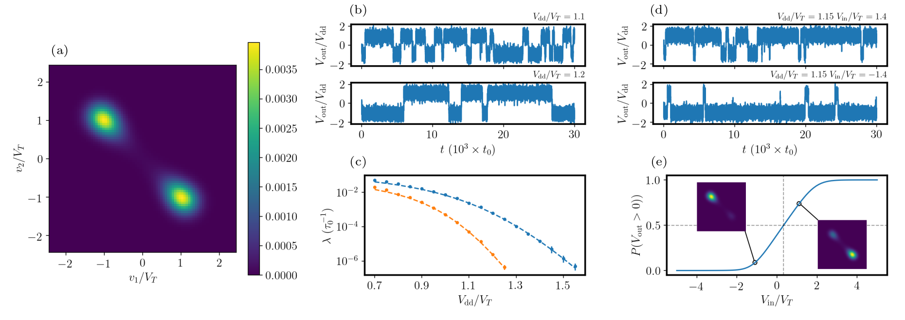
We propose a full-CMOS design for a -bit that is self-sufficient: its stochastic behavior is due to the intrinsic thermal noise, so no external source of noise is necessary. Also, while in -bits based on MTJs the transition rate or error probability is fixed by the fabrication process (for a given temperature), our design allows to control this parameter on the fly by just changing the power voltage. The basic circuit is shown in Figure 13 and is composed of two coupled NOT gates as in regular SRAM cells. The logical circuit of Figure 13-(a) has two stable states: and , or and . The corresponding CMOS implementation of Figure 13-(b) has two degrees of freedom: the voltages and (or alternatively, the charges and ) at the output of each inverter. We consider to be the output used to monitor the state of the bit. If the powering voltage is above a critical value (that for can be found to be freitas2021 ), then the deterministic equations for the circuit have two possible steady solutions, which correspond to the two stable logical states of Figure 13-(a). At the stochastic level, they correspond to two metastable NESSs, for which or , respectively. A stochastic model for the circuit of Figure 13-(b) can be built as before, by employing the mapping of Figure 8 and constructing the rates associated to each transistor with the procedure of Section IV.3. In this case this is done automatically by a custom software package, that is also able to deal with general circuits SSE_github . The steady state distribution can be obtained by constructing the generator of the master equation in Eq. (12) (truncated to some maximum number of charges), and computing its eigenvector of zero eigenvalue, as shown in Figure 14-(a). Also, the corresponding stochastic dynamics can be simulated with the Gillespie algorithm. In this way we can generate stochastic trajectories. For example, in Figure 14-(b) we show two trajectories for different values of the power voltage. To obtain those results we considered the following parameters: (room temperature), and . Crucially, these values of capacitances are compatible to what is achieved in modern sub-nm fabrication processes zheng2016 . Also, for simplicity we took , and as before the parameters and of the transistors just fix the time scale . We clearly observe random transitions, or errors, between the two metastable NESSs, and that the transition or error rate depends on the power voltage . This is easily understood: frequent random transitions are expected whenever the standard deviation of the fluctuations around the output voltage, which can be estimated as , is comparable to the mean value . Thus, one can control the transition rate by changing the powering voltage or, for fixed , by changing the temperature and or the size of the transistors (which modifies the capacitances and ). Indeed, to a very good approximation, the waiting time between transitions is exponentially distributed, , and the transition rate can be seen to scale as to dominant order in freitas2021 . Note that for the previous parameters is of order one at room temperature, but that it increases as the square root of the size of the transistors. Therefore, the transition rate decreases exponentially in the size of the transistors. As a consequence, the exploitation of these naturally ocurring fluctuations as a resource at room temperature is only a real possibility for highly scaled, state of the art fabrication processes, as the ones considered above. The error rate can be computed from the trajectories generated by the Gillespie algorithm, or also by spectral methods as explained in freitas2021 . The results are shown in Figure 14-(c), for two different scales.
To complete the construction of the -bit it is necessary to provide a mechanism to bias its output. There are different ways to achieve this, and here we will focus on the circuit of Figure 13-(c), where the biasing circuit is colored. It works as follows. A bias voltage is coupled to the outputs of the two inverters which form the core of the -bit through the drain-source channel of two transistors. The transistor influencing the output of the first inverter is an nMOS, while the one influencing the output of the second inverter is a pMOS. Both transistors have their bodies grounded, such that their activation depends only on the gate-body voltage (the Poisson rates corresponding to this configuration are discussed in the supplementary material). For , both transistors are equaly activated and the output of both inverters is very weakly biased towards in . For , conduction through the nMOS is enhanced, while it is suppressed for the pMOS, and therefore only the output of the first inverter is biased towards . In that case the symmetry between the two possible metastable NESSs ( or ) is broken in favour of the one with . The situation is reversed for . In Figure 14-(d) we show two sample trajectories of the output voltage for a positive and a negative value of the input voltage . We see that is indeed biased and spends more time around positive or negative values, respectively. The parameters of the transistors are the same as before, with the exception that the specific current of the transistors in the biasing circuit is one order of magnitude lower than the others (). Also, we considered a bias voltage . In Figure 14-(e) we show how the probability of the output being positive depends on the input voltage. We see that is indeed given by a sigmoidal function of , similar to the typical activation functions considered in artificial neural networks. Note however that, due to the asymmetric I-V curves of the transistors in the biasing circuit, the balanced case is not achieved at but for a slightly positive .
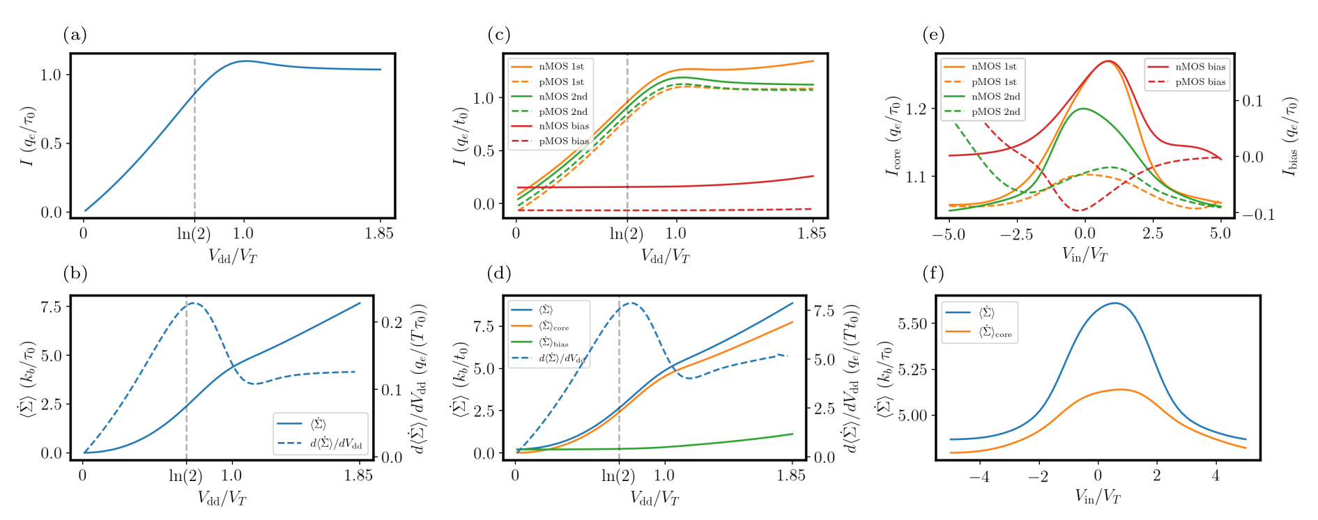
We now analyze the energy consumption of the -bit. For this we obtain the steady state distribution as before, and compute the mean values of current and heat rates associated to each transistor according to Eqs. (57) and (61), respectively. By symmetry, for the circuit consituting the core of the bit in Figure 13-(b), the steady state electric current through all the four transistor is the same, and its dependence on is shown in Figure 15-(a). We see that it increases monotonously for low powering voltages, and that it develops a peak right after the transition into bistability (at ), after which it settles to a constant value. This maximum in the current close to the transition into bistability is associated to the ocurrence of errors or transitions between different NESSs: each switching event involves the relaxation of previously stored charge, which adds up to the continuous flow of charge in each NESS. This is also seen in Figure 15-(b), where we plot the entropy production rate and its derivative with respect to the powering voltage. Since we are considering steady state conditions, we have that , where is the rate of heat dissipation in the n/pMOS transistor of the first or second inverter. Interestingly, we see that the transition to bistability is signaled by a maximum in the derivative of with respect to .
In Figure 15-(c) we show all the currents for the full circuit of Figure 13-(c), including the bias circuit, for and . We see that the behaviour of the currents through the transistor in the core circuit is qualitatively similar as the previous case, although the currents are naturally not all equal anymore. In Figure 15-(d) we show the total entropy production and its derivative for the full circuit. In this case we split the total entropy production rate as , where , and are the rate entropy production rates corresponding the the bit core and biasing circuits ( is the rate of heat dissipation in the nMOS or pMOS biasing transistor). We see that the transition to bistability is still signaled by a maximum in the derivative of , and that the dissipation associated to the biasing circuit is a small fraction of the total one.
Finally, the behaviour with respect to the input voltage with fixed powering voltage and bias voltage is shown in Figures 15-(e-f). In Figure 15-(f), we see that the entropy production rate has a maximum value at zero bias. This is again due to the ocurrence of transitions between different NESSs, which of course decrease when the bias increases in any direction.
The average total dissipated heat per generated bit is given by . It is interesting to note that for transitions generated by intrinsic thermal noise, decreases as the speed or transition rate increases. For example, by reducing the powering voltage (always above ), the total rate of heat dissipation decreases (Figures 15-(b) and (d)), while the transition rate increases exponentially (Figures 14-(c)), and therefore decreases exponentially. For we have an average dissipated heat per generated bit in the order of . This can be compared to the MTJ -bit in borders2019 , that requires an energy of per random bit, two orders of magnitude higher than the previous estimation.
VIII Discussion
We have presented a formalism for the construction of stochastic models of non-linear electronic circuits in a thermodynamically consistent way. Devices with arbitrary I-V curves can be described, provided that their current fluctuations display shot noise. A complete analysis of the stochastic thermodynamics of these models was carried out. The relevant thermodynamic potentials were identified, and the different contributions to the irreversible entropy production were characterized. All these quantities were extended to individual trajectories, based on which we presented different detailed and integral fluctuation theorems. As a first application, we have constructed a stochastic model of a subthreshold CMOS inverter, or NOT gate. We have shown how to analytically find the steady state of the resulting master equation. Based on that solution, we analyzed how the non-equilibrium thermal fluctuations induce modifications in the transfer function of the gate. Also, we showed how to compute the full counting statistics of the current fluctuations and in that way illustrated a detailed fluctuation theorem. Finally, we proposed a full-CMOS design of a probabilistic bit, or binary stochastic neuron, in which intrinsic thermal noise is exploited as a resource to generate random bits of information in a controllable way. The energy consumption of our design is several times lower than in previous proposals.
Of course, the formalism has some limitations, which are important to discuss here. In first place, only devices displaying shot noise can be described. This excludes, for example, regular resistors or MOS transistors in general modes of operation. In addition, it is not possible to describe inertial effects (i.e., inductances). These could be included at the price of mixing discrete and continuous variations of charge. Nevertheless, there is little practical motivation for this, since it is difficult to integrate inductances in nanoscale electronic circuits philip2017 , and therefore inertial effects might only be relevant at extremely high frequencies. There are other possible extensions of the formalism, which are however less relevant, since they capture effects that can be actually emulated with the formalism as presented here. For example, although the stochastic dynamics we have considered is Markovian, non-Markovian effects can be described by considering a given circuit as a part of a larger one (something known as ‘Markovian embedding’). Finally, although we have not focused on single electron devices, our formalism can be directly applied to them. In that context, there are “cotunneling” effects (events in which two or more transitions happen at the same time, possibly leaving the state of the circuit unchanged) that can become relevant in the Coulomb blockade regime and our formalism does not take into accountwasshuber2012
Our work offers a connection between different subjects and communities. It shows how to employ the methods of stochastic thermodynamics and single electron devices in order to model other kinds of circuits that are traditionally given a deterministic description, which is later supplemented by an approximate treatment of the noise. In this way we can describe the fluctuations in those circuits on a rigorous basis. This is relevant and timely, given the impressive reduction in the size of CMOS circuits, and the need for new energy-efficient computing paradigms. On the other hand, the great versatility in the fabrication and control of electronic circuits makes them an excellent platform to study complex phenomena in statistical physics and non-equilibrium thermodynamics. Thus, our formalism also offers a valuable bridge between theory and experiment. In the future it could be interesting to explore the connection between the low-level description we propose here and the more abstract treatments of stochastic thermodynamics of complex circuits in Refs. boyd2018 ; wolpert2020 , in particular under which conditions the fundamental bounds that they obtained can be approached within a given technology.
After finishing this work we became aware of a recent article rezaei2020 , in which a similar stochastic description is employed to compute the error rate of a low-power SRAM memory cell. It should be noted that the transition rates employed in that article are actually not thermodynamically consistent, i.e., they do not respect the local detailed balance conditions.
IX Acknowledgments
J. C. D. thanks Denis Flandre and Léopold Van Brandt for helpful comments and discussions. J. C. D. and M.E. acknowledge funding from the project PDR 40003438 “TheCirco” on Thermodynamics of Circuits for Computation, funded by the F.R.S.-FNRS (Belgium) and FNR (Luxembourg). N. F. and M. E. acknowledge funding from the European Research Council, project NanoThermo (ERC-2015-CoGAgreement No. 681456), and from the FNR CORE program, project NTEC (C19/MS/13664907). J. C. D. was also funded by the FNR Program No. INTER/MOBILITY/18/12987626.
References
- [1] Camilo Mora, Randi L Rollins, Katie Taladay, Michael B Kantar, Mason K Chock, Mio Shimada, and Erik C Franklin. Bitcoin emissions alone could push global warming above 2 c. Nature Climate Change, 8(11):931–933, 2018.
- [2] Eric Masanet, Arman Shehabi, Nuoa Lei, Sarah Smith, and Jonathan Koomey. Recalibrating global data center energy-use estimates. Science, 367(6481):984–986, 2020.
- [3] Laszlo B Kish. End of Moore’s law: thermal (noise) death of integration in micro and nano electronics. Physics Letters A, 305(3-4):144–149, 2002.
- [4] Akram S Sadek, Konstantin Nikolić, and Michael Forshaw. Parallel information and computation with restitution for noise-tolerant nanoscale logic networks. Nanotechnology, 15(1):192, 2003.
- [5] Shankar Krishnan, Suresh V Garimella, Gregory M Chrysler, and Ravi V Mahajan. Towards a thermal Moore’s law. IEEE Transactions on advanced packaging, 30(3):462–474, 2007.
- [6] Laszlo B Kish. Noise-based logic: Binary, multi-valued, or fuzzy, with optional superposition of logic states. Physics Letters A, 373(10):911–918, 2009.
- [7] Tara Julia Hamilton, Saeed Afshar, Andre van Schaik, and Jonathan Tapson. Stochastic electronics: A neuro-inspired design paradigm for integrated circuits. Proceedings of the IEEE, 102(5):843–859, 2014.
- [8] Alexei O Orlov, Ismo K Hänninen, César O Campos-Aguillón, Rene Celis-Cordova, Michael S McConnell, Gergo P Szakmany, Cameron C Thorpe, Brian T Appleton, Graham P Boechler, Craig S Lent, et al. Experimental tests of the landauer principle in electron circuits, and quasi-adiabatic computing systems. In Energy Limits in Computation, pages 177–230. Springer, 2019.
- [9] Elahe Rezaei, Marco Donato, William R Patterson, Alexander Zaslavsky, and R Iris Bahar. Fundamental thermal limits on data retention in low-voltage CMOS latches and SRAM. IEEE Transactions on Device and Materials Reliability, 2020.
- [10] Krishna V Palem. Energy aware computing through probabilistic switching: A study of limits. IEEE Transactions on Computers, 54(9):1123–1137, 2005.
- [11] Suresh Cheemalavagu, Pinar Korkmaz, Krishna V Palem, Bilge ES Akgul, and Lakshmi N Chakrapani. A probabilistic CMOS switch and its realization by exploiting noise. In IFIP International Conference on VLSI, pages 535–541, 2005.
- [12] Jie Han and Michael Orshansky. Approximate computing: An emerging paradigm for energy-efficient design. In 2013 18th IEEE European Test Symposium (ETS), pages 1–6. IEEE, 2013.
- [13] Kerem Yunus Camsari, Rafatul Faria, Brian M Sutton, and Supriyo Datta. Stochastic p-bits for invertible logic. Physical Review X, 7(3):031014, 2017.
- [14] William A Borders, Ahmed Z Pervaiz, Shunsuke Fukami, Kerem Y Camsari, Hideo Ohno, and Supriyo Datta. Integer factorization using stochastic magnetic tunnel junctions. Nature, 573(7774):390–393, 2019.
- [15] Jan Kaiser, Rafatul Faria, Kerem Y Camsari, and Supriyo Datta. Probabilistic circuits for autonomous learning: A simulation study. Frontiers in Computational Neuroscience, 14, 2020.
- [16] Ya M Blanter and Markus Büttiker. Shot noise in mesoscopic conductors. Physics reports, 336(1-2):1–166, 2000.
- [17] Richard McFee. Self-rectification in diodes and the second law of thermodynamics. American Journal of Physics, 39(7):814–820, 1971.
- [18] NG Van Kampen. Non-linear thermal fluctuations in a diode. Physica, 26(8):585–604, 1960.
- [19] Laurens Weiss and Wolfgang Mathis. A thermodynamical approach to noise in non-linear networks. International Journal of Circuit Theory and Applications, 26(2):147–165, 1998.
- [20] John L Wyatt Jr and Geoffrey J Coram. Nonlinear device noise models: Thermodynamic requirements. Technical report, 1997.
- [21] John L Wyatt and Geoffrey J Coram. Nonlinear device noise models: Satisfying the thermodynamic requirements. IEEE transactions on electron devices, 46(1):184–193, 1999.
- [22] Léon Brillouin. Can the rectifier become a thermodynamical demon? Physical Review, 78(5):627, 1950.
- [23] Han-Ngee Tan and J Wyatt. Thermodynamics of electrical noise in a class of nonlinear RLC networks. IEEE transactions on circuits and systems, 32(6):540–558, 1985.
- [24] Massimiliano Esposito, Upendra Harbola, and Shaul Mukamel. Nonequilibrium fluctuations, fluctuation theorems, and counting statistics in quantum systems. Reviews of modern physics, 81(4):1665, 2009.
- [25] Michele Campisi, Peter Hänggi, and Peter Talkner. Colloquium: Quantum fluctuation relations: Foundations and applications. Reviews of Modern Physics, 83(3):771, 2011.
- [26] Christopher Jarzynski. Equalities and inequalities: Irreversibility and the second law of thermodynamics at the nanoscale. Annu. Rev. Condens. Matter Phys., 2(1):329–351, 2011.
- [27] Udo Seifert. Stochastic thermodynamics, fluctuation theorems and molecular machines. Reports on progress in physics, 75(12):126001, 2012.
- [28] Riccardo Rao and Massimiliano Esposito. Detailed fluctuation theorems: A unifying perspective. Entropy, 20(9):635, 2018.
- [29] Ken Sekimoto. Stochastic energetics, volume 799. Springer, 2010.
- [30] Xue-Juan Zhang, Hong Qian, and Min Qian. Stochastic theory of nonequilibrium steady states and its applications. Part I. Physics Reports, 510(1-2):1–86, 2012.
- [31] Riccardo Rao and Massimiliano Esposito. Conservation laws shape dissipation. New Journal of Physics, 20(2):023007, 2018.
- [32] S Ciliberto. Experiments in stochastic thermodynamics: Short history and perspectives. Physical Review X, 7(2):021051, 2017.
- [33] Riccardo Rao and Massimiliano Esposito. Conservation laws and work fluctuation relations in chemical reaction networks. The Journal of chemical physics, 149(24):245101, 2018.
- [34] JMR Parrondo and B Jiménez de Cisneros. Energetics of Brownian motors: a review. Applied Physics A, 75(2):179–191, 2002.
- [35] R Van Zon, S Ciliberto, and EGD Cohen. Power and heat fluctuation theorems for electric circuits. Physical review letters, 92(13):130601, 2004.
- [36] Nicolas Garnier and Sergio Ciliberto. Nonequilibrium fluctuations in a resistor. Physical Review E, 71(6):060101, 2005.
- [37] Sergio Ciliberto, Alberto Imparato, Antoine Naert, and Marius Tanase. Heat flux and entropy produced by thermal fluctuations. Physical review letters, 110(18):180601, 2013.
- [38] Nahuel Freitas, Jean-Charles Delvenne, and Massimiliano Esposito. Stochastic and quantum thermodynamics of driven RLC networks. Phys. Rev. X, 10:031005, Jul 2020.
- [39] Michel H Devoret, Daniel Estève, Hermann Grabert, G-L Ingold, Hugues Pothier, and Cristian Urbina. Effect of the electromagnetic environment on the Coulomb blockade in ultrasmall tunnel junctions. Physical review letters, 64(15):1824, 1990.
- [40] Christoph Wasshuber. Computational single-electronics. Springer Science & Business Media, 2012.
- [41] DA Bagrets and Yu V Nazarov. Full counting statistics of charge transfer in Coulomb blockade systems. Physical Review B, 67(8):085316, 2003.
- [42] DV Averin and KK Likharev. Coulomb blockade of single-electron tunneling, and coherent oscillations in small tunnel junctions. Journal of low temperature physics, 62(3-4):345–373, 1986.
- [43] D Ali and H Ahmed. Coulomb blockade in a silicon tunnel junction device. Applied physics letters, 64(16):2119–2120, 1994.
- [44] David Andrieux and Pierre Gaspard. Fluctuation theorem for transport in mesoscopic systems. Journal of Statistical Mechanics: Theory and Experiment, 2006(01):P01011, 2006.
- [45] Massimiliano Esposito, Upendra Harbola, and Shaul Mukamel. Fluctuation theorem for counting statistics in electron transport through quantum junctions. Physical Review B, 75(15):155316, 2007.
- [46] Gregory Bulnes Cuetara, Massimiliano Esposito, and Pierre Gaspard. Fluctuation theorems for capacitively coupled electronic currents. Physical Review B, 84(16):165114, 2011.
- [47] JV Koski, T Sagawa, OP Saira, Y Yoon, A Kutvonen, P Solinas, M Möttönen, T Ala-Nissila, and JP Pekola. Distribution of entropy production in a single-electron box. Nature Physics, 9(10):644, 2013.
- [48] Gregory Bulnes Cuetara and Massimiliano Esposito. Double quantum dot coupled to a quantum point contact: a stochastic thermodynamics approach. New Journal of Physics, 17(9):095005, 2015.
- [49] Jukka P Pekola. Towards quantum thermodynamics in electronic circuits. Nature Physics, 11(2):118–123, 2015.
- [50] Giuliano Benenti, Giulio Casati, Keiji Saito, and Robert S Whitney. Fundamental aspects of steady-state conversion of heat to work at the nanoscale. Physics Reports, 694:1–124, 2017.
- [51] Jiayin Gu and Pierre Gaspard. Microreversibility, fluctuations, and nonlinear transport in transistors. Physical Review E, 99(1):012137, 2019.
- [52] Christian C Enz and Eric A Vittoz. Charge-based MOS transistor modeling. John Wiely & Sons Inc, 68, 2006.
- [53] Yannis Tsividis and Colin McAndrew. Operation and Modeling of the MOS Transistor. Oxford Univ. Press, 2011.
- [54] Rahul Sarpeshkar, Tobias Delbruck, and Carver A Mead. White noise in MOS transistors and resistors. IEEE Circuits and Devices Magazine, 9(6):23–29, 1993.
- [55] Jiayin Gu and Pierre Gaspard. Stochastic approach and fluctuation theorem for charge transport in diodes. Physical Review E, 97(5):052138, 2018.
- [56] Jiayin Gu and Pierre Gaspard. Counting statistics and microreversibility in stochastic models of transistors. Journal of Statistical Mechanics: Theory and Experiment, 2020(10):103206, 2020.
- [57] David H Wolpert. The stochastic thermodynamics of computation. Journal of Physics A: Mathematical and Theoretical, 52(19):193001, 2019.
- [58] Takahiro Sagawa. Second law, entropy production, and reversibility in thermodynamics of information. In Energy limits in computation, pages 101–139. Springer, 2019.
- [59] Charles H Bennett. The thermodynamics of computation—a review. International Journal of Theoretical Physics, 21(12):905–940, 1982.
- [60] Charles H Bennett and Rolf Landauer. The fundamental physical limits of computation. Scientific American, 253(1):48–57, 1985.
- [61] Takahiro Sagawa. Thermodynamic and logical reversibilities revisited. Journal of Statistical Mechanics: Theory and Experiment, 2014(3):P03025, 2014.
- [62] Takahiro Sagawa and Masahito Ueda. Minimal energy cost for thermodynamic information processing: measurement and information erasure. Physical review letters, 102(25):250602, 2009.
- [63] Jordan M Horowitz and Massimiliano Esposito. Thermodynamics with continuous information flow. Physical Review X, 4(3):031015, 2014.
- [64] Krzysztof Ptaszyński and Massimiliano Esposito. Thermodynamics of quantum information flows. Physical review letters, 122(15):150603, 2019.
- [65] Erik Aurell, Krzysztof Gawedzki, Carlos Mejia-Monasterio, Roya Mohayaee, and Paolo Muratore-Ginanneschi. Refined second law of thermodynamics for fast random processes. Journal of statistical physics, 147(3):487–505, 2012.
- [66] Tim Schmiedl and Udo Seifert. Optimal finite-time processes in stochastic thermodynamics. Physical review letters, 98(10):108301, 2007.
- [67] David A Sivak and Gavin E Crooks. Thermodynamic metrics and optimal paths. Physical review letters, 108(19):190602, 2012.
- [68] Schuyler B Nicholson, Luis Pedro Garcia-Pintos, Adolfo del Campo, and Jason R Green. Time–information uncertainty relations in thermodynamics. Nature Physics, 16(12):1211–1215, 2020.
- [69] Giovanni Diana, G Baris Bagci, and Massimiliano Esposito. Finite-time erasing of information stored in fermionic bits. Physical Review E, 87(1):012111, 2013.
- [70] Patrick R Zulkowski and Michael R DeWeese. Optimal finite-time erasure of a classical bit. Physical Review E, 89(5):052140, 2014.
- [71] Karel Proesmans, Jannik Ehrich, and John Bechhoefer. Finite-time landauer principle. Physical Review Letters, 125(10):100602, 2020.
- [72] Shiqi Sheng, Tim Herpich, Giovanni Diana, and Massimiliano Esposito. Thermodynamics of majority-logic decoding in information erasure. Entropy, 21(3):284, 2019.
- [73] Alexander B Boyd, Dibyendu Mandal, and James P Crutchfield. Thermodynamics of modularity: Structural costs beyond the landauer bound. Physical Review X, 8(3):031036, 2018.
- [74] David Wolpert and Artemy Kolchinsky. The thermodynamics of computing with circuits. New Journal of Physics, 2020.
- [75] Alice Wang, Benton H Calhoun, and Anantha P Chandrakasan. Sub-threshold design for ultra low-power systems, volume 95. Springer, 2006.
- [76] Jin-Woo Han, Jae Sub Oh, and M Meyyappan. Vacuum nanoelectronics: Back to the future? - Gate insulated nanoscale vacuum channel transistor. Applied Physics Letters, 100(21):213505, 2012.
- [77] David H Ackley, Geoffrey E Hinton, and Terrence J Sejnowski. A learning algorithm for Boltzmann machines. Cognitive science, 9(1):147–169, 1985.
- [78] Yoshua Bengio, Nicholas Léonard, and Aaron Courville. Estimating or propagating gradients through stochastic neurons for conditional computation. arXiv preprint arXiv:1308.3432, 2013.
- [79] Kashif Nawaz, Léopold Van Brandt, Itamar Levi, François-Xavier Standaert, and Denis Flandre. A security oriented transient-noise simulation methodology: Evaluation of intrinsic physical noise of cryptographic designs. Integration, 68:71–79, Sep 2019.
- [80] Andries J Scholten, Ronald Van Langevelde, Luuk F Tiemeijer, and Dick BM Klaassen. Compact modeling of noise in CMOS. In IEEE Custom Integrated Circuits Conference 2006, pages 711–716. IEEE, 2006.
- [81] Matteo Polettini and Massimiliano Esposito. Irreversible thermodynamics of open chemical networks. I. emergent cycles and broken conservation laws. The Journal of chemical physics, 141(2):07B610_1, 2014.
- [82] Leon O Chua, Charles A Desoer, and Ernest S Kuh. Linear and nonlinear circuits. McGraw-Hill College, 1987.
- [83] Peter Hanggi and Peter Jung. Bistability in active circuits: Application of a novel fokker-planck approach. IBM Journal of Research and Development, 32(1):119–126, 1988.
- [84] Jordan M Horowitz. Diffusion approximations to the chemical master equation only have a consistent stochastic thermodynamics at chemical equilibrium. The Journal of chemical physics, 143(4):044111, 2015.
- [85] Masao Doi. Second quantization representation for classical many-particle system. Journal of Physics A: Mathematical and General, 9(9):1465, 1976.
- [86] Alexandre Lefevre and Giulio Biroli. Dynamics of interacting particle systems: stochastic process and field theory. Journal of Statistical Mechanics: Theory and Experiment, 2007(07):P07024, 2007.
- [87] Hugo Touchette. The large deviation approach to statistical mechanics. Physics Reports, 478(1-3):1–69, 2009.
- [88] Alexandre Lazarescu, Tommaso Cossetto, Gianmaria Falasco, and Massimiliano Esposito. Large deviations and dynamical phase transitions in stochastic chemical networks. The Journal of Chemical Physics, 151(6):064117, 2019.
- [89] Rolf Landauer. Solid-state shot noise. Physical Review B, 47(24):16427, 1993.
- [90] Theodore A Fulton and Gerald J Dolan. Observation of single-electron charging effects in small tunnel junctions. Physical review letters, 59(1):109, 1987.
- [91] William Shockley. The theory of p-n junctions in semiconductors and p-n junction transistors. Bell System Technical Journal, 28(3):435–489, 1949.
- [92] MJ Kirton and MJ Uren. Noise in solid-state microstructures: A new perspective on individual defects, interface states and low-frequency (1/f) noise. Advances in Physics, 38(4):367–468, 1989.
- [93] Xiaoming Chen, Lin Wang, Boxun Li, Yu Wang, Xin Li, Yongpan Liu, and Huazhong Yang. Modeling Random Telegraph Noise as a Randomness Source and its Application in True Random Number Generation. IEEE Trans. Comput. Aided Des. Integr. Circuits Syst., 35(9):1435–1448, Dec 2015.
- [94] Léopold Van Brandt, Bahak Kazemi Esfeh, Valeriya Kilchytska, and Denis Flandre. Robust Methodology for Low-Frequency Noise Power Analyses in Advanced MOS Transistors. 2019 Joint International EUROSOI Workshop and International Conference on Ultimate Integration on Silicon (EUROSOI-ULIS), pages 1–4, Apr 2019.
- [95] E Paladino, YM Galperin, G Falci, and BL Altshuler. 1/f noise: Implications for solid-state quantum information. Reviews of Modern Physics, 86(2):361, 2014.
- [96] Hermann Grabert and Michel H Devoret. Single charge tunneling: Coulomb blockade phenomena in nanostructures, volume 294. Springer Science & Business Media, 2013.
- [97] Peng Zheng. Advanced MOSFET structures and processes for sub-7 nm CMOS technologies. PhD thesis, UC Berkeley, 2016.
- [98] Tommaso Cossetto. Problems in nonequilibrium fluctuations across scales: A path integral approach, Oct 2020. [Online; accessed 19. Feb. 2021].
- [99] Nahuel Freitas, Karel Proesmans, and Massimiliano Esposito. Reliability and entropy production in non-equilibrium electronic memories. arXiv, Mar 2021.
- [100] Massimiliano Esposito and Christian Van den Broeck. Second law and landauer principle far from equilibrium. EPL (Europhysics Letters), 95(4):40004, 2011.
- [101] Takahiro Sagawa. Thermodynamics of information processing in small systems. Progress of theoretical physics, 127(1):1–56, 2012.
- [102] Juan MR Parrondo, Jordan M Horowitz, and Takahiro Sagawa. Thermodynamics of information. Nature physics, 11(2):131–139, 2015.
- [103] Paul M Riechers. Transforming metastable memories: The nonequilibrium thermodynamics of computation. arXiv preprint arXiv:1808.03429, 2018.
- [104] Thomas Speck and Udo Seifert. Integral fluctuation theorem for the housekeeping heat. Journal of Physics A: Mathematical and General, 38(34):L581, 2005.
- [105] Artemy Kolchinsky and David H Wolpert. Entropy production and thermodynamics of information under protocol constraints. arXiv preprint arXiv:2008.10764, 2020.
- [106] U Seifert. Fluctuation theorem for a single enzym or molecular motor. EPL (Europhysics Letters), 70(1):36, 2005.
- [107] André M Timpanaro, Giacomo Guarnieri, John Goold, and Gabriel T Landi. Thermodynamic uncertainty relations from exchange fluctuation theorems. Physical review letters, 123(9):090604, 2019.
- [108] Andrew Lucas. Ising formulations of many NP problems. Frontiers in Physics, 2:5, 2014.
- [109] Sabpreet Bhatti, Rachid Sbiaa, Atsufumi Hirohata, Hideo Ohno, Shunsuke Fukami, and SN Piramanayagam. Spintronics based random access memory: a review. Materials Today, 20(9):530–548, 2017.
- [110] Bilge ES Akgul, Lakshmi N Chakrapani, Pinar Korkmaz, and Krishna V Palem. Probabilistic cmos technology: A survey and future directions. In 2006 IFIP international conference on very large scale integration, pages 1–6. IEEE, 2006.
- [111] Nahuel Freitas. Stochastic single electronics (SSE). https://github.com/nfreitas/SSE, 2020.
- [112] Timothy M Philip and Matthew J Gilbert. High-performance nanoscale topological inductor. In 2017 75th Annual Device Research Conference (DRC), pages 1–2. IEEE, 2017.
See pages 1,2,3,4,5,6,7 of ./supplementary_material.pdf