Two-dimensional ferromagnetic semiconductor VBr3 with tunable anisotropy
Abstract
Two-dimensional (2D) ferromagnets (FMs) have attracted widespread attention due to their prospects in spintronic applications. Here we explore the electronic structure and magnetic properties of the bulk and monolayer of VBr3 in the honeycomb lattice, using first-principles calculations, crystal field level analyses, and Monte Carlo simulations. Our results show that VBr3 bulk has the 2 (=1) ground state and possesses a small orbital moment and weak in-plane magnetic anisotropy. Those results well explain the recent experiments. More interestingly, we find that a tensile strain on the semiconducting VBr3 monolayer tunes the ground state into 11 and thus produces a large orbital moment and a strong out-of-plane anisotropy. Then, the significantly enhanced FM superexchange and single ion anisotropy (SIA) would raise from 20 K for the bare VBr3 monolayer to 100-115 K under a 2.5-5 strain. Therefore, VBr3 would be a promising 2D FM semiconductor with a tunable anisotropy.
I Introduction
Bulk materials with a van der Waals (vdW) gap, readily to be cleaved, attract a large volume of attention due to their thickness-dependent electronic and magnetic properties.Huang et al. (2017); Gong et al. (2017); Deng et al. (2018); Chen et al. (2019); Li et al. (2019); Song et al. (2019); Klein et al. (2019); Huang et al. (2020); Kim et al. (2019a) In principle, long-range magnetic order at finite temperature is prohibited in two-dimensional (2D) isotropic Heisenberg spin systems according to the Mermin-Wagner theorem.Mermin and Wagner (1966) Very recently, 2D ferromagnetism (FM) has been observed in atomically thin CrI3 (Ref. 1) and Cr2Ge2Te6 (Ref. 2). The FM ordering is remarkably retained in CrI3 monolayer with the Curie temperature =45 K. These discoveries have brought about intriguing magnetism and have invoked extensive research in 2D FMs. This opens a new avenue to spintronic applications, such as spin valves,Cardoso et al. (2018) spin filters,Klein et al. (2018); Song et al. (2018) and data storage.Soumyanarayanan et al. (2016)
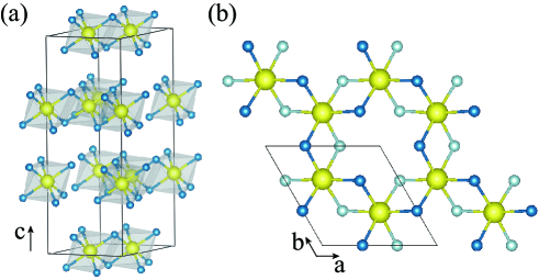
Vanadium trihalides are vdW materials with a layered honeycomb structure, see Fig. 1. They are of current interest due to their similarity with CrI3, and they may also be promising candidates for 2D FMs.Huang et al. (2017); Kong et al. (2019a, b); Tian et al. (2019); Son et al. (2019) It is worth noting that FM CrI3, with a closed Cr3+ 3 shell, has a quenched orbital moment, and that its magnetic anisotropy comes from an exchange anisotropy induced by the spin-orbit coupling (SOC) of the heavy I orbitals and their hybridization with Cr .Lado and Fernandez-Rossier (2017); Kim et al. (2019b) In contrast, the open V3+ 2 shell in vanadium trihalides may carry an unquenched orbital moment and achieve a single ion anisotropy (SIA) via the V3+ SOC. This seems to account for the hard perpendicular FM with 50 K observed in VI3 bulkKong et al. (2019b); Tian et al. (2019); Son et al. (2019) and even the Ising FM in VI3 monolayer.Yang et al. (2020)
Among vanadium trihalides, VBr3 bulk is a layered antiferromagnetic (AF) semiconductor with the Neel temperature =26.5 K, the effective magnetic moment of 2.6 per V3+ ion, and the optical band gap slightly larger than 1 eV. And it has a stronger in-plane magnetic susceptibility than the out-of-plane one below .Kong et al. (2019a) In this article, we study the electronic and magnetic structures of VBr3 bulk and monolayer from first-principles calculations, crystal field level analyses, and Monte Carlo simulations. We find that the V3+ ions are in the 2 =1 state in the trigonal crystal field of the honeycomb lattice, and they have an intralayer FM coupling but one order of magnitude weaker interlayer magnetic coupling. Moreover, each V3+ ion carries a small in-plane orbital moment due to a mixing of the and states by V3+ SOC. Then, VBr3 bulk would rather have a weak parallel magnetic anisotropy as detailed below, and this explains the experimental anisotropic magnetic susceptibilities. Note that VBr3 monolayer, if cleaved, would be a 2D FM semiconductor with a weak parallel magnetic anisotropy and 20 K. More interestingly, VBr3 monolayer would turn into the 11 ground state under a tensile strain. Then it carries a large out-of-plane orbital moment and has a strong SIA driven perpendicular magnetic anisotropy. As a result, the significantly enhanced FM superexchange and perpendicular anisotropy would raise up to 100-115 K under a 2.5-5 strain. Therefore, VBr3 monolayer would be an appealing 2D FM semiconductor with a tunable anisotropy.
II Computational Details
VBr3 bulk material (space group R) has the A-B-C layer stacking sequence via vdW interactions, see Fig. 1. Edge-sharing VBr6 octahedra form a honeycomb lattice within each layer. For V3+ ions with the local octahedral coordinates, the global trigonal crystal field splits the triplet into the singlet and the doublet. The global coordinate system was used in the following calculations, with the axis along the direction of the local VBr6 octahedra and along the direction. Then the wave functions under the trigonal crystal field can be written as
| (1) | ||||
Density functional calculations (DFT) were carried out using the full-potential augmented plane wave plus local orbital code (Wien2k).Blaha et al. The lattice parameters of VBr3 bulk (monolayer) were optimized to be ==6.299 Å (6.342 Å) and =18.110 Å, which are almost the same (within 1.5%) as the experimental ones of ==6.371 Å and =18.376 Å.Kong et al. (2019a) A vacuum slab of 10 Å was set along the -axis for the monolayer. The muffin-tin sphere radii were chosen to be 2.5 Bohr for V atoms and 2.2 Bohr for Br. The plane-wave cut-off energy of 12 Ry was set for the interstitial wave functions, and a -mesh was used for integration over the Brillouin zone. Note that VBr3 is a narrow band (less than 1 eV, see below) strongly correlated system, and the electron correlation was included in our calculations, using the local spin density approximation plus Hubbard (LSDA+) method,Anisimov et al. (1993) with the typical values of Hubbard =3.9 eV and Hund exchange =0.9 eV. The obtained semiconducting solution with the band gap of 1.2 eV well reproduces the experimental band gap. We also use crystal-field level diagrams and superexchange pictures to understand the electronic and magnetic properties. The spin-orbit coupling (SOC) was included for V and Br orbitals by the second-variational method with scalar relativistic wave functions. To clearly see the crystal field effect, exchange splitting, electron correlation, and the crucial SOC effects, we present and discuss below the spin restricted LDA, spin polarized LSDA, LSDA+, and LSDA+SOC+ calculations. Monte Carlo simulations on a spin matrix have also been performed to estimate the Curie temperature of VBr3 monolayer using Metropolis method.Metropolis and Ulam (1949)
III Results and Discussion
VBr3 Bulk
We first investigate the VBr3 bulk for which the experimental results are available for comparison. Our LDA calculations find the - crystal field splitting of about 1.5 eV, see Fig. 2(a). The singlet and doublet out of each forms a partially occupied narrow band (less than 1 eV) crossing Fermi level and they are almost degenerate. The Br state lies in the range of 2-6 eV below Fermi level, and it has a notable hybridization with V , particularly the strong one with the orbital. Owing to the narrow band localization effect, the V electrons prefer to be spin polarized and they form =1 state as indicated by LSDA calculations. As seen in Fig. 2(b), only the up-spin and bands are partially occupied, giving the total spin moment of 2 for each V3+ ion.
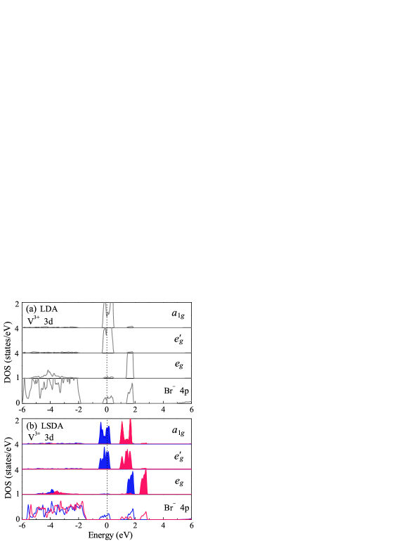
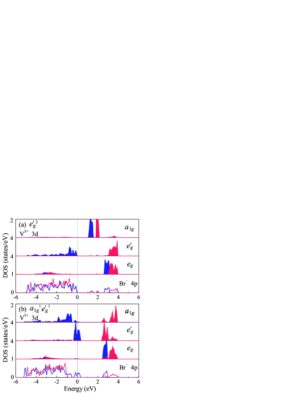
Moreover, when the electron correlation effect is included for this narrow band system as done in our LSDA+ calculations, a semiconducting solution is obtained with the closed 2 subshell of the V3+ ions, see Fig. 3(a). The semiconducting gap of 1.2 eV is well comparable with the experimental value slightly larger than 1 eV. As seen in Table I, the =1 V3+ ion has the local spin moment of 1.86 reduced by the V -Br hybridization. In contrast, another metallic solution (11), with the half-filled band crossing Fermi level, was also obtained in our LSDA+ calculations, see Fig. 3(b). However, this metallic solution turns out to be much more unstable against the above semiconducting one by about 312.5 meV/fu, see Table I. Therefore, the V3+ 2 solution seems to be the ground state of VBr3 bulk. For this orbital state, our LSDA+ calculations find that the intralayer FM state is more stable than the AF state by 7.9 meV/fu, but the interlayer magnetic coupling is one order of magnitude weaker (see below) and is out of concern (and beyond the scope) of this work.
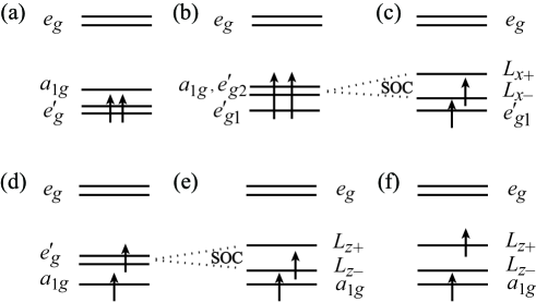
To analyze the above results, we plot in Fig. 4 the crystal field level diagrams of the V3+ ions. As the singlet and doublet are almost degenerate, the two possible solutions, 2 and 11 are displayed in Figs. 4(a) and 4(d), respectively. The former is semiconducting but the latter is metallic, given by the above LSDA+ calculations. However, when the SOC is included, the and can be mixed. Then the SOC can produce an in-plane orbital moment, for example, an orbital moment along the axis by mixing the and [see Eq. 1 and Figs. 4(b)-4(c)]. In contrast, the mixing between the and states by the SOC will produce the states with an orbital moment along the axis. These possible solutions, as shown in Figs. 4(b), 4(c), 4(e), and 4(f), will be obtained in the following LSDA+SOC+ calculations.
| States | ||||
|---|---|---|---|---|
| LSDA+ | 2 | 0.0 | 1.86 | |
| 2 (AF) | 7.9 | 1.84 | ||
| 11 | 312.5 | 2.04 | ||
| LSDA+SOC+ | 2, | 0.0 | 1.87 | 0.23 |
| 2, (AF) | 8.2 | 1.84 | 0.21 | |
| 2, | 2.3 | 1.86 | 0.00 | |
| 11, | 14.5 | 1.91 | 1.15 | |
| 11, | 26.7 | 1.90 | 1.11 | |
| 11, | 54.1 | 1.91 | 1.14 |
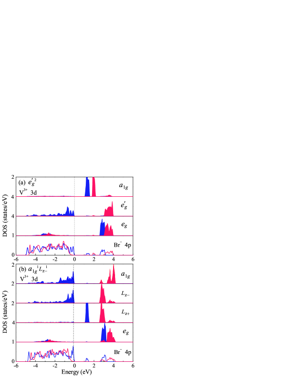
We collect our LSDA+SOC+ results in Table I. The formal 2 state now has an in-plane orbital moment of –0.23 , in addition to the spin moment of 1.87 . This semiconducting solution is very similar to that one by LSDA+, see Figs. 3(a) and 5(a). The small in-plane orbital moment tends to align via SOC the spin moment also in the plane. If the magnetization is assumed to be along the axis for the formal 2 state, no orbital moment will appear as the SOC split states are both fully occupied. Then only the spin moment of 1.86 persists. As a result, the formal 2 state with the small in-plane orbital moment gains a partial SOC energy, producing the easy planar magnetization with the magnetic anisotropy energy of 2.3 meV/fu, see Table I. Moreover, this state favors the intralayer FM coupling, with the intralayer AF state being higher in energy by 8.2 meV/fu. This intralayer FM coupling will be further elucidated below for the VBr3 monolayer. In contrast, the interlayer magnetic coupling is much weaker due to the vdW gap and here the layered FM and AF states differ in total energy only by 0.8 meV/fu.
To determine the electronic ground state of the VBr3 bulk, we also achieve several other possible solutions using the constrained LSDA+SOC+ calculations with the initialized configurations Ou and Wu (2014); Ou et al. (2015) for those different orbital states shown in Fig. 4. For example, when we start from the 11 state and now perform LSDA+SOC+ calculations, we will get either 11 state or 11. The former solution is now semiconducting [see Fig. 5(b)], in sharp contrast to the 11 metallic one given by LSDA+ [see Fig. 3(b)]. This semiconducting 11 state lies in total energy higher than the (2 ) ground state by 14.5 meV/fu, and has the local spin moment of 1.91 and the orbital moment of –1.15 (see Table I), both of which are along the axis but antiparallel. If we force the orbital moment to be parallel to the spin moment as done for the 11 solution, the increasing total energy (54.1 vs 14.5 meV/fu) allows us to estimate the SOC strength parameter 40 meV for V3+ electrons. Moreover, by an equal mixing via SOC between the and states, the 11 state can also be obtained in our LSDA+SOC+ calculations, which give a spin (orbital) moment of 1.90 (–1.11) both along the axis. However, this solution is higher in total energy than the (2 ) ground state by 26.7 meV/fu.
The above results lead us to a conclusion that the vdW bulk material VBr3 is a narrow band magnetic semiconductor. It is in the formal V3+ 2 =1 ground state and has a small in-plane orbital moment and magnetic anisotropy energy of 2.3 meV/fu. The spin and orbital moments prefer to align in the plane, and those V3+ spins are FM coupled in the plane. The V3+ =1 spin moment and a small antiparallel orbital moment account for the experimental effective magnetic moment of 2.6 , Kong et al. (2019a) which is slightly reduced from the pure spin contribution 2=2.83 . Moreover, considering the intralayer FM coupling and the one order of magnitude weaker interlayer magnetic coupling and the experimental layered AF state with =26.5 K, we can explain the experimentally observed magnetic anisotropy Kong et al. (2019a): At 50 K and above, the magnetic susceptibilities are almost the same for the applied magnetic field parallel or perpendicular to the plane; At 1.8 K, the in-plane magnetic susceptibility is much stronger than the out-of-plane one. This is because at 1.8 K, VBr3 bulk is in the layered AF state with the spins lying in the plane. As the interlayer AF coupling (0.8 meV/fu) is weaker than the magnetic anisotropy (2.3 meV/fu), those spins are more susceptible to the in-plane magnetic field and can flip in the plane, giving a stronger parallel magnetic susceptibility. At 50 K and above, the magnetic anisotropy (2.3 meV) is already overcome, and thus the system is in the isotropic paramagnetic state. As such, our results have well explained the experimental magnetic behavior of VBr3 bulk.
VBr3 Monolayer
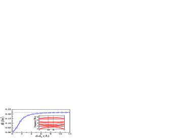
The vdW material VBr3 has an intralayer FM coupling and a much weaker interlayer magnetic coupling, and thus it could be a potential 2D FM semiconductor which is desirable for spintronics. The calculated cleavage energy of 0.22 J/m2 for the VBr3 monolayer (see Fig. 6), using the DFT+vdW correction,Lee et al. (2010) is well comparable with that of 0.3 J/m2 for the CrI3 monolayer which is already exfoliated from its bulk. The dynamical stability of VBr3 monolayer is also indicated by our phonon calculations, Kresse and Furthmuller (1996); Togo and Tanaka (2015) which show no imaginary frequency phonons through the whole Brillouin zone. Hence, we now turn to the VBr3 monolayer and focus on its electronic and magnetic properties by carrying out LSDA+SOC+ calculations, superexchange analyses, and Monte Carlo simulations of its 2D FM order. The tensile strain effect of the 2D lattice is also studied, and it is capable of tuning the orbital state of the V3+ ions and turns out to significantly enhance the FM order with tunable superexchange and magnetic anisotropy.
The electronic structure of the VBr3 monolayer is very similar to that of the bulk, and therefore the DOS results for the monolayer are not shown here again. We list the major results in Table II from the LSDA+SOC+ calculations of the most concern. All the solutions for VBr3 monolayer are semiconducting. For the bare monolayer without strain, the electronic ground state is again the formal 2 state, which carries the local V3+ spin moment of 1.87 and a small in-plane orbital moment of –0.23 . As a result, the easy magnetization direction lies in the plane, with the magnetic anisotropy energy of 2.0 meV/fu. Moreover, this 2 ground state prefers the FM coupling within the 2D V3+ lattice, which is more stable than the AF state by 7.9 meV/fu. In addition, for the 11 state, it has a large out-of-plane orbital moment of –1.15 (antiparallel to the spin moment of 1.91 ) but is less stable than the 2 FM ground state by 12.0 meV/fu. Therefore, the bare VBr3 monolayer is a FM semiconductor with a parallel magnetic anisotropy.
| Strain | States | |||
|---|---|---|---|---|
| 0% | 2, | 0.0 | 1.87 | 0.23 |
| 2, (AF) | 7.9 | 1.84 | 0.21 | |
| 2, | 2.0 | 1.86 | 0.00 | |
| 2, (AF) | 9.7 | 1.84 | 0.00 | |
| 11, | 12.0 | 1.91 | 1.15 | |
| 2.5% | 11, | 0.0 | 1.92 | 1.16 |
| 11, (AF) | 31.8 | 1.87 | 1.22 | |
| 11, | 15.0 | 1.92 | 0.12 | |
| 11, (AF) | 47.3 | 1.87 | 0.10 | |
| 2, | 80.9 | 1.87 | 0.44 | |
| 5% | 11, | 0.0 | 1.92 | 1.17 |
| 11, (AF) | 38.4 | 1.87 | 1.25 | |
| 11, | 13.9 | 1.93 | 0.09 | |
| 11, (AF) | 52.4 | 1.87 | 0.08 | |
| 2, | 141.6 | 1.87 | 0.41 | |
| Strain | ||||
| 0%, | 1.9 | 2.6 | 20 | |
| 2.5%, | 15.2 | 10.8 | 100 | |
| 5%, | 13.9 | 12.8 | 115 |
The electronic state and magnetism of 2D materials may be tuned by a strain. Baskurt et al. (2020); Iyikanat et al. (2018); Bacaksiz et al. (2020) For VBr3 monolayer, a tensile strain would flatten the VBr6 octahedron along the axis (i.e., the local [111] direction of the VBr3 octahedron) and lowers the singlet off the doublet. Then, the 11 would become the ground state for the =1 V3+ ion, and it would have a large perpendicular orbital moment and a strong single ion anisotropy (SIA) in the SOC split ground state 11. To verify this, we perform LSDA+SOC+ calculations for the VBr3 monolayer under the tensile strain of 2.5% and 5%. For the 2.5% strain, both the formal 2 and 11 solutions are achieved in our calculations. The 2 solution has a spin moment of 1.87 and an in-plane orbital moment of –0.44 , and however, it has a much higher total energy than the 11 solution by 80.9 meV/fu. Indeed, here the 11 solution becomes the ground state as expected, and it has a spin moment of 1.92 and a large out-of-plane orbital moment of –1.16 , see Table II. This orbital moment tends via the SOC to align the spin moment along the axis, and if the spin moment flips into the plane, there would be a large SOC energy cost. As a result, the 11 ground state has a large perpendicular magnetic anisotropy, which is up to 15.0 meV/fu by our LSDA+SOC+ calculations. For the 5% strain, the 11 ground state becomes even more stable against the formal 2 state by 141.6 meV/fu, and the resultant perpendicular magnetic anisotropy is 13.9 meV/fu. Apparently, the tensile strain can effectively modify the electronic ground state of VBr3 monolayer and tune its magnetic anisotropy, from the formal 2 ground state and a moderate parallel magnetic anisotropy to the 11 ground state and a large perpendicular anisotropy.
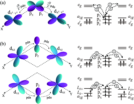
Moreover, the tensile strain turns out to enhance the FM coupling significantly: For the bare VBr3 monolayer, the 2 ground state prefers the FM superexchange, which is more stable than the AF one by 7.9 meV/fu. For the monolayer under 2.5% strain, the 11 ground state has a much enhanced FM stability against the AF by 31.8 meV/fu, which is up to 38.4 meV/fu for 5% strain, see Table II. Now we provide a picture to understand why the FM superexchange is largely enhanced under the tensile strain, i.e., upon the electronic state transition from 2 to 11. To better discuss the electron hopping, here we use the local coordinates of the VBr3 octahedra. Then the V wave functions can be written as follows
Having the early transition metal V and the strong V -Br covalency, VBr3 could be at the border of Mott-Hubbard type and charge-transfer one. Khomskii (2014) When considering the charge-transfer behavior, the V Br V virtual hoppings (forth and back, large type) with double holes on the ligand Br orbitals are important, see Fig. 7(a), and this would give a FM superexchange which sees no difference between the 2 and 11 states. However, in the Mott-Hubbard regime, the V3+ ions in the 2 or 11 state would undergo much different FM superexchange. Considering an effective electron hopping in two neighboring V3+ ions via the common ligand Br orbital [see Fig. 7(b)], with the strength where is the charge transfer energy, the effective hopping between the orbitals of two neighboring V3+ ions is parameterized as 2 (defined as 2), and so is the hopping in between the and orbitals, and the rest inter-site hopping within the is =, see more details in Refs. 21 and 33. Then, the superexchange FM stability against AF via the occupied to unoccupied is (10)(2) in the 11 state, being more than doubled as compared with that of (4)(2) in the 2 state.
As shown above, the tensile strain significantly enhances the FM superexchange of the VBr3 monolayer and the SIA. Therefore, the FM ordering temperature of the VBr3 monolayer would be largely increased by the tensile strain. We carry out Monte Carlo simulations to estimate the , using the following spin Hamiltonian
where the first term stands for the SIA [positive (negative) for the easy (hard) -axis magnetization], the second term describes the Heisenberg isotropic exchange [positive (negative) for FM (AF) coupling], and the last term represents the anisotropic exchange [positive (negative) for the easy (hard) -axis magnetization]. The sum over runs over all V3+ sites with =1 in the honeycomb lattice, and over the three nearest neighbors of each . The parameters , , and are determined by calculating the four magnetic states, i.e., the FM and AF states with the in-plane or out-of-plane magnetization, see Table II.

For the VBr3 monolayer, we find that is one to two orders of magnitude smaller than and , showing a minor contribution from the anisotropic exchange. Thus, the 2D FM order of VBr3 monolayer is mainly stabilized by the FM superexchange and SIA. (This is different from the well studied CrI3 monolayer, where the Cr3+ ion has a closed 3 shell and has a negligible SIA, and the notable anisotropic exchange comes from the strong SOC of the heavy I orbitals and strong Cr -I hybridization. Lado and Fernandez-Rossier (2017); Kim et al. (2019b)) Note that for VBr3 monolayer under the tensile strain, the FM parameter is significantly enhanced, and the SIA parameter changes from a small negative value to a large positive one, see Table II. For the bare VBr3 monolayer, its is about 20 K (see Fig. 8), according to our Monte Carlo simulations, due to the relatively small SIA and the relatively weak FM superexchange. In strong contrast, the VBr3 monolayer has a significantly increasing up to 100-115 K under the 2.5-5% tensile strain, due to the strong FM coupling and strong SIA. Therefore, we propose that the VBr3 monolayer under a tensile strain would be a promising 2D FM semiconductor, which calls for an experimental verification.
IV Summary
In summary, using density functional calculations including SOC effect and electron correlation, and the crystal field and superexchange pictures as well, we find that the vdW material VBr3 is in the formal 2 ground state and has an intralayer FM coupling and a weak parallel magnetic anisotropy. These results well account for the experimental magnetic behavior of the bulk VBr3. More interestingly, the VBr3 monolayer has a well comparable or even smaller cleavage energy as compared with other known 2D materials, and it is proposed to be a 2D FM semiconductor. We find that the bare VBr3 monolayer has 20 K estimated from our Monte Carlo simulations, which is due to the relatively weak FM coupling and the small parallel magnetic anisotropy. In strong contrast, a tensile strain turns the VBr3 monolayer into the 11 ground state. Then, the VBr3 monolayer under the 2.5-5% tensile strain has a largely increasing up to 100-115 K, which arises from the significantly enhanced FM superexchange and the strong perpendicular magnetic anisotropy. Thus we conclude that VBr3 monolayer under a tensile strain has a largely tunable magnetic anisotropy and quite high and it would be a promising 2D FM semiconductor.
Acknowledgements
This work was supported by the NSF of China (Grant No. 11674064) and by the National Key Research and Development Program of China (Grant No. 2016YFA0300700).
References
- Huang et al. (2017) B. Huang, G. Clark, E. Navarro-Moratalla, D. R. Klein, R. Cheng, K. L. Seyler, D. Zhong, E. Schmidgall, M. A. McGuire, D. H. Cobden, W. Yao, D. Xiao, P. Jarillo-Herrero, and X. Xu, Nature 546, 270 (2017).
- Gong et al. (2017) C. Gong, L. Li, Z. Li, H. Ji, A. Stern, Y. Xia, T. Cao, W. Bao, C. Wang, Y. Wang, Z. Q. Qiu, R. J. Cava, S. G. Louie, J. Xia, and X. Zhang, Nature 546, 265 (2017).
- Deng et al. (2018) Y. Deng, Y. Yu, Y. Song, J. Zhang, N. Z. Wang, Z. Sun, Y. Yi, Y. Z. Wu, S. Wu, J. Zhu, J. Wang, X. H. Chen, and Y. Zhang, Nature 563, 94 (2018).
- Chen et al. (2019) W. Chen, Z. Sun, Z. Wang, L. Gu, X. Xu, S. Wu, and C. Gao, Science 366, 983 (2019).
- Li et al. (2019) T. Li, S. Jiang, N. Sivadas, Z. Wang, Y. Xu, D. Weber, J. E. Goldberger, K. Watanabe, T. Taniguchi, C. J. Fennie, K. F. Mak, and J. Shan, Nat. Mater. 18, 1303 (2019).
- Song et al. (2019) T. Song, Z. Fei, M. Yankowitz, Z. Lin, Q. Jiang, K. Hwangbo, Q. Zhang, B. Sun, T. Taniguchi, K. Watanabe, M. A. McGuire, D. Graf, T. Cao, J.-H. Chu, D. H. Cobden, C. R. Dean, D. Xiao, and X. Xu, Nat. Mater. 18, 1298 (2019).
- Klein et al. (2019) D. R. Klein, D. MacNeill, Q. Song, D. T. Larson, S. Fang, M. Xu, R. A. Ribeiro, P. C. Canfield, E. Kaxiras, R. Comin, and P. Jarillo-Herrero, Nat. Phys. 15, 1255 (2019).
- Huang et al. (2020) B. Huang, J. Cenker, X. Zhang, E. L. Ray, T. Song, T. Taniguchi, K. Watanabe, M. A. McGuire, D. Xiao, and X. Xu, Nat. Nanotechnol. 15, 212 (2020).
- Kim et al. (2019a) H. H. Kim, B. Yang, S. Li, S. Jiang, C. Jin, Z. Tao, G. Nichols, F. Sfigakis, S. Zhong, C. Li, S. Tian, D. G. Cory, G.-X. Miao, J. Shan, K. F. Mak, H. Lei, K. Sun, L. Zhao, and A. W. Tsen, Proc. Natl. Acad. Sci. U. S. A. 116, 11131 (2019a), https://www.pnas.org/content/116/23/11131.full.pdf .
- Mermin and Wagner (1966) N. D. Mermin and H. Wagner, Phys. Rev. Lett. 17, 1133 (1966).
- Cardoso et al. (2018) C. Cardoso, D. Soriano, N. A. Garcia-Martinez, and J. Fernandez-Rossier, Phys. Rev. Lett. 121, 067701 (2018).
- Klein et al. (2018) D. R. Klein, D. MacNeill, J. L. Lado, D. Soriano, E. Navarro-Moratalla, K. Watanabe, T. Taniguchi, S. Manni, P. Canfield, J. Fernandez-Rossier, and P. Jarillo-Herrero, Science 360, 1218 (2018).
- Song et al. (2018) T. Song, X. Cai, M. W.-Y. Tu, X. Zhang, B. Huang, N. P. Wilson, K. L. Seyler, L. Zhu, T. Taniguchi, K. Watanabe, M. A. McGuire, D. H. Cobden, D. Xiao, W. Yao, and X. Xu, Science 360, 1214 (2018).
- Soumyanarayanan et al. (2016) A. Soumyanarayanan, N. Reyren, A. Fert, and C. Panagopoulos, Nature 539, 509 (2016).
- Kong et al. (2019a) T. Kong, S. Guo, D. Ni, and R. J. Cava, Phys. Rev. Mater. 3, 084419 (2019a).
- Kong et al. (2019b) T. Kong, K. Stolze, E. I. Timmons, J. Tao, D. Ni, S. Guo, Z. Yang, R. Prozorov, and R. J. Cava, Adv. Mater. 31, 1808074 (2019b), https://onlinelibrary.wiley.com/doi/pdf/10.1002/adma.201808074 .
- Tian et al. (2019) S. Tian, J.-F. Zhang, C. Li, T. Ying, S. Li, X. Zhang, K. Liu, and H. Lei, J. Am. Chem. Soc. 141, 5326 (2019).
- Son et al. (2019) S. Son, M. J. Coak, N. Lee, J. Kim, T. Y. Kim, H. Hamidov, H. Cho, C. Liu, D. M. Jarvis, P. A. C. Brown, J. H. Kim, C.-H. Park, D. I. Khomskii, S. S. Saxena, and J.-G. Park, Phys. Rev. B 99, 041402(R) (2019).
- Lado and Fernandez-Rossier (2017) J. L. Lado and J. Fernandez-Rossier, 2D Mater. 4, 035002 (2017).
- Kim et al. (2019b) D.-H. Kim, K. Kim, K.-T. Ko, J. Seo, J. S. Kim, T.-H. Jang, Y. Kim, J.-Y. Kim, S.-W. Cheong, and J.-H. Park, Phys. Rev. Lett. 122, 207201 (2019b).
- Yang et al. (2020) K. Yang, F. Fan, H. Wang, D. I. Khomskii, and H. Wu, Phys. Rev. B 101, 100402(R) (2020).
- (22) P. Blaha, K. Schwarz, G. Madsen, D. Kvasnicka, and J. Luitz, “Wien2k package,” http://www.wien2k.at.
- Anisimov et al. (1993) V. I. Anisimov, I. V. Solovyev, M. A. Korotin, M. T. Czyżyk, and G. A. Sawatzky, Phys. Rev. B 48, 16929 (1993).
- Metropolis and Ulam (1949) N. Metropolis and S. Ulam, J. Am. Stat. Assoc. 44, 335 (1949).
- Ou and Wu (2014) X. Ou and H. Wu, Sci. Rep. 4, 4609 (2014).
- Ou et al. (2015) X. Ou, H. Wang, F. Fan, Z. Li, and H. Wu, Phys. Rev. Lett. 115, 257201 (2015).
- Lee et al. (2010) K. Lee, E. D. Murray, L. Kong, B. I. Lundqvist, and D. C. Langreth, Phys. Rev. B 82, 081101(R) (2010).
- Kresse and Furthmuller (1996) G. Kresse and J. Furthmuller, Phys. Rev. B 54, 11169 (1996).
- Togo and Tanaka (2015) A. Togo and I. Tanaka, Scr. Mater. 108, 1 (2015).
- Baskurt et al. (2020) M. Baskurt, I. Eren, M. Yagmurcukardes, and H. Sahin, Appl. Surf. Sci. 508, 144937 (2020).
- Iyikanat et al. (2018) F. Iyikanat, M. Yagmurcukardes, R. T. Senger, and H. Sahin, J. Mater. Chem. C 6, 2019 (2018).
- Bacaksiz et al. (2020) C. Bacaksiz, M. Yagmurcukardes, F. M. Peeters, and M. V. Milosevic, 2D Mater. 7, 025029 (2020).
- Khomskii (2014) D. I. Khomskii, Transition Metal Compounds (Cambridge University Press, 2014).