Defect-tuned colossal cryo-thermopower in FeSb2.
Abstract
FeSb2 hosts higher known values of thermopower in nature. By changing the amount of defects in different FeSb2 crystals here we show that thermopower maxima change between relatively small 14 V/K and colossal values of about 20 mV/K. Defects also cause rather weak but important monoclinic distortion of the crystal structure . Whereas defects of both Fe and Sb atoms are observed, Sb-defficiency at Sb11 sites of space group is significant, revealing the source of the in-gap states that govern thermopower size. The broad distribution of the in-gap states of Fe orbital character gives rise to thermopower consistent with the electronic diffusion mechanism but only a well-defined in-gap state drives the colossal enhancement above the electronic difusion limit. The absence of Sb along [010] promotes stronger quasi 1D Fe orbital overlap, which induces more anisotropy in the electronic structure and triggers the quasi-1D conductivity in optics and electricity.
Thermoelectric materials exploit thermoelectric effect where temperature difference is converted into electric power and vice versa Bell ; Snyder . Progress in cryo-thermoelectric materials discovery has been much slower when compared to materials used above the room temperature Heremans ; He ; Herbert . This is because at low temperature additional complexity arises since electronic correlations cannot be neglected Tomczak ; Palsson ; KoshibaeW . Also, in the figure of merit where is temperature, is thermopower and () are electrical (thermal) conductivities, cryogenic temperature is inevitably small Snyder . Therefore, a cryo-thermoelectric material must maximize its thermoelectric power factor () where thermopower provides considerable contribution.
The iron diantimonide FeSb2 is a narrow-gap semiconductor that features colossal thermopower and thermoelectric power factor at cryogenic temperatures Cedomir ; Cedomir2 ; Bentien ; JieQ . It has been proposed that colossal thermopower in FeSb2 is of electronic origin Sun ; Sun1 . Consequently multiband electronic correlation are important for the enhancement of the diffusion thermopower up to about 1 mV/K, much higher than expected from the Mott formula where values of the order of 10 V/K are commonly observed Cutler ; Tomczak1 . Recently it has been argued that enhancement above the diffusion limit into values of the order of 10 mV/K is due to phonon drag Tomczak1 ; Takahashi . Although the importance of the in-gap states to the thermopower was recognized, the origin of the in-gap states and the role it takes in determining the thermopower remain controversial Tomczak1 ; Matsuura . The possible origin from the impurities in the Fe and Sb metals was studied and the electrical transport below 40 K shows sensitivity to even ppm-level impurities Takahashi1 . While the sample-dependence electrical resistivity was explained, the effect of these impurities to the large Seebeck coefficient and the origin of the quasi-1D conductivity in optics and electrical transport were not well understood Cedomir ; Homes .
Whereas atomic defects have been extensively used to enhance high-temperature thermoelectric performance by lowering phonon thermal conductivity in the figure of merit Biswa ; KimK , tiny amount of defects are not expected to distort crystal structure and dramatically tune thermopower values Takahashi1 . In this work we show that in correlated electron thermoelectric FeSb2, colossal thermopower arises from Sb vacancy-induced changes in the crystal structure and associated in-gap states through the phonon-drag effectBattiato . Moreover, our results indicate that thermopower and the quasi-1D behavior in conductivity are tunable by Sb defects.
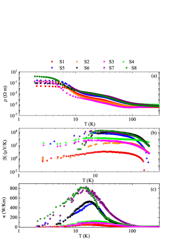
Figure 1(a-b) presents electronic and thermal transport difference among eight crystals of FeSb2 grown under somewhat different conditions Supplement . Crystals S7 and S8 have about 1-2 order of magnitude higher electrical resistivity when compared to crystals S1-S3 in temperature region (10 - 20) K [Figure 1(a)]. Moreover, crystals S1-S3 have clear weak (semi)metallic resistivity in 60 K to 300 K temperature region. Low-temperature thermopower shows large variation [Fig. 1(b)]; maxima change by several orders of magnitude from S1 (14 V/K) to S8 (20 mV/K). Figure 1(c) shows thermal conductivity vs temperature for samples S1-S8. The increase more than 8 times from S1 to S8 which reflects the increase scattering of phonons and the decrease of the phonon mean free path Supplement .
Thermally activated resistivity above 50 K [Figure 1(a)] stems from the intrinsic energy gap consistent with the electronic structure calculations; however the resistivity shoulder in the region of around 10 K is a fingerprint of the defect-induced in-gap impurity states Battiato ; Sun3 ; Takahashi2 . Recently proposed physical mechanism of colossal thermoelectricity in FeSb2 links the in-gap states to phonon-drag effect Battiato ; Matsuura . The effects of defects in scattering the phonons and decreasing the phonon-drag effect are discussed in the supplemental material. Although defect-induced in-gap states are necessary to the large Seebeck coefficient through phonon-drag effect, excessive defects is harmful to achieve this lrage Seebeck coefficient. The magnetoresistance (MR) changes in FeSb2 should arise only in the temperature range where the in-gap band provides dominant contribution to electronic transport; a single in-gap band gives only one peak in MR Battiato . In agreement with previous observation Sun3 , MR in high-thermopower crystals S6 and S8 shows one peak associated with a well-defined in-gap state [Figure 2(a)]. This is in contrast with MR in low-thermopower crystals S1 and S3 where broad MR is observed, consistent with a rather broad distribution of multiple in-gap states Battiato . Another important observation is that the driver of colossal thermopower-related in-gap states is unlikely to be in Fe-rich Fe1+xSb2-x as postulated in Ref. 20. High thermopower crystal S8 shows the absence of the Curie tail in contrast to low-thermopower crystal S3 [Fig. 2(b)]. By fitting the tail of S3 using the Curie law [Fig. 2(c)], concentration of excess Fe is about 4 atomic percents. The in-gap states emerge from different cause, as we show below.
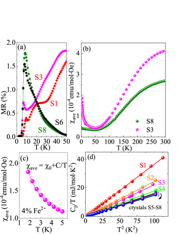
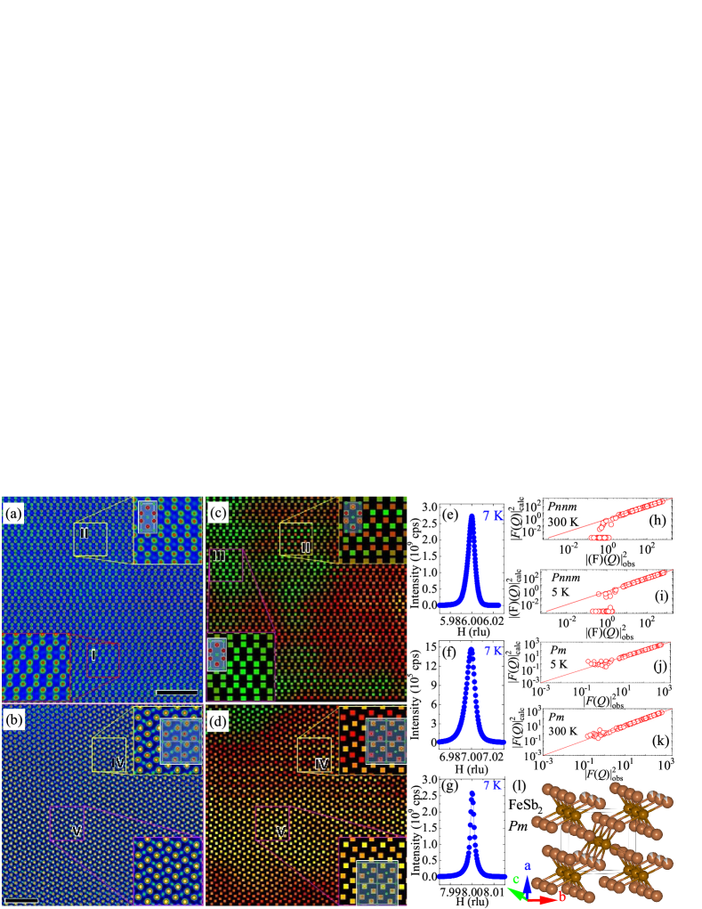
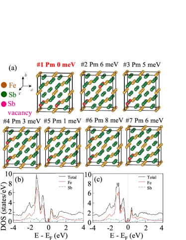
Figure 2(d) shows heat capacity of S1-S8 crystals. We observe a general trend of the slope change associated with Debye temperature. In general, vacancy formation energy is related to Debye temperature: , where is a constant, is the vacancy formation energy, M and are atomic mass and volume Mukherjee ; March . Low vacancy formation energy is consistent with higher number of vacancies for low thermopower crystals (e.g. S1) when compared to high thermopower crystals (e.g. S8). Results are summarized in Table S1 Supplement .
To shed light on the vacancy defects we performed high resolution scanning transmission electron microscopy (STEM) with a high angle annular dark field (HAADF) detector as its contrast is proportional to Z1.7 along the atom column, where Z is the atomic number. Figures 3 (a,b) show the STEM-HAADF images taken from low thermopower S3 and high thermopower S8 samples, respectively. The strong and weak dots in the images correspond to Sb and Fe atoms, respectively. The atomic arrangement in the images is consistent with the FeSb2 structure with symmetry, as shown in the insets where the atomic projections are embedded in the magnified image. Due to the Z-contrast nature of the STEM-HAADF image, the peak intensity of each dot can be used to count the atoms along the column LeBeau . Higher peak intensity indicates more atoms along the column, while weaker peak intensity indicates less atoms, thus more vacancies along the column. It is seen that the peak intensity of Fe is quite uniform in the S8 [Fig. 3(b)], indicating the relative uniform distribution of Fe. However, the peak intensity of Fe varies in S3, e.g. there are less Fe in area I than that in area II, as shown in the magnified image in the insets of Figure 3(a). We also observe Sb intensity variation, indicating the variation of Sb occupancies. The Sb occupancies or vacancies can be better resolved by refining each Sb column peak with the second order polynomial function. Fig. 3(c,d) shows the peak intensity maps of Sb for S3 and S8, respectively. There are four Sb atoms in a FeSb2 unit cell. In sample S3, the Sb peak intensity is the same in some area [inset III in Fig. 3(c)], consistent with the symmetry. In the other area, however, the Sb peak intensity changes periodically, and orders along [010] direction, as shown in the inset II in Fig. 3(c), where two Sb peaks (orange squares) are stronger than the other two Sb (green squares) within the unit cell. This indicates the ordering of Sb vacancies and reduction of the symmetry in this area. In [100] projection orange and red spheres represent high and low Sb occupancy, embedded in the inset II. The size of the phase separation clusters with Sb vacancy ordering is about a few nanometers. These clusters are similar to the nanoprecipitates observed in PbTe-AgSbTe2 system Hsu ; Ke . They induce additional phonon scattering, thus reduce the thermal conductivity and phonon mean free path of S3. For crystal S8, the Sb vacancy ordering is observed in nearly all locations and also along [010] direction. In area IV [Fig. 3(d)], two Sb peaks (orange) are stronger than the other two Sb (red). While in the area V, one Sb peak (yellow square) is stronger than the other three Sb (orange squares).
Sb vacancy ordering results in a -forbidden peak observed in single crystal synchrotron X-ray diffraction [Figure 3(e-g)], consistent with weak structural distortion observed in neutron diffraction measurements [Figure 3 (h-k)]. Neutron diffraction shows presence of weak (h,0,l), h + l = odd and (0,k,l), k + l = odd type Bragg reflections, which are forbidden in crystal structure previously refined for the stoichiometric FeSb2 Cedomir ; Cedomir2 ; Hagg . The presence of these forbidden reflections hints that the symmetry of the crystal lattice is lower. Comprehensive structural refinement [Figure 4(h-k), Tables S2-S5 Supplement ] indicate that one of the two Sb sites, which are equivalent in space group shows displacive monoclinic distortions and site deficiency. This induces very subtle change in the structural symmetry (), making two Sb sites inequivalent, i. e. Sb1 site is fully occupied while Sb11 site contains substantial number of vacancies that do not change with temperature [Fig. 3 (l)]. We find that the Sb11 site is 0.82(2) occupied while both Fe sites are 0.94(2) occupied; the chemical vacancies do not change with temperature whereas intensity of -forbidden peaks at 300 K is 2/3 of that at 5 K Supplement .
The FeSb6 octahedra are edge-sharing along the shortest lattice parameter 3.194 . Closer inspection of unit cell shows that the Sb11 atomic sites labeled with arrows [Fig. S1] are also separated by the lattice parameter length 3.194 along the edge-sharing octahedral direction. However, weak metallic conductivity at high temperature for low thermopower crystals [Figure 1(a)] is along the orthogonal, 6.536 lattice parameter direction where distance of Sb11 to Fe is shorter [-direction in Fig. 3(l), see also Fig. S1] Cedomir ; Supplement ; Hu1 . This is consistent with TEM-observed vacancy order direction [Figure 3 (a-d)] and quasi 1D conductivity in optics Perucchi ; Homes . It should be noted that occupancy of Fe orbital () translates into different unit cell parameter along the orbital overlap. Higher (lower) occupancy corresponds to larger (shorter) unit cell parameter Hull ; Hulliger . Detailed comparison of sample S3 and S8 crystallography by laboratory single crystal X-ray diffraction shows longer lattice parameter in low thermopower sample S3 (Table S6 Supplement ), implying differences in Fe orbital occupation. A picture emerges where Sb11 vacancies create Fe-derived conducting in-gap states due to short Fe-Sb11 hopping distance (Fig. S1 Supplement ). Low vacancy formation energy, i.e. higher vacancy content in low-thermopower crystals such as S3 [Fig. 2(d)], promotes stronger quasi 1D Fe orbital overlap due to the absence of Sb along [010], weak metallicity and metal-insulator transition JieQ . As we show below, first-principle calculations support this scenario.
GW+DMFT calculations show that bands associated with quasi 1D dispersion along 6.536 are Fe-derived: bottom of the conduction band is dominated by Fe xy orbital whereas top of the valence bands is dominated by Fe xz/yz bands Homes . First-principle calculation results [Fig. 4(a)] confirm that structure distortion to space group is energetically favorable in Sb-defficient FeSb2 unit cell. However, the Sb vacancies also induce Fe dangling bonds that might influence electronic structure though conducting impurity band at the Fermi level for high Sb defect concentration.
To explore how Sb vacancy and its ratio affect the electronic structure of FeSb2, we studied two cases of Sb vacancy ratios: one and two Sb vacancies in a 2 2 3 super-cell of FeSb2. To simulate the experimental situation, we only consider Sb vacancies at the Sb11 site. Hence, Sb vacancies for both cases occupy the Sb11 site only, and they correspond to 91.7 and 83.3 of Sb11 occupancy, respectively, where the case of two Sb vacancies is close to the experimental Sb11 occupancy, 82 at T = 300 K. For the case of one Sb vacancy, there is only one symmetrically non-equivalent configuration for introducing one Sb vacancy at the Sb11 site in the 2 2 3 super-cell. On the other hand, for the case of two Sb vacancies, there are 7 symmetrically non-equivalent configurations. We have considered all of the 7 configurations and found that two Sb vacancies is the configuration that is the most energetically stable [Fig. 4(a)]. From now on, we only focus on the most stable configuration for each Sb vacancy ratio.
Figure 4(b) shows the density of states (DOS) of the most stable configurations for both Sb vacancy ratios. The Sb vacancies give rise to Fe dangling bonds that lead to metallic impurity bands at the Fermi level. The impurity bands have a dominant -orbital character of Fe possessing the dangling bonds. We would like to note that the DFT calculation with the modified Becke-Johnson (mBJ) exchange potential method gives a clear bulk gap of 0.25 eV in FeSb2 without any vacancies. As depicted in Fig. 4(b), the case of two Sb vacancies shows broader bandwidth of the metallic impurity band than that of one Sb vacancy, indicating that as the Sb vacancy ratio increases, the metallic impurity band is more dispersive. The case of one Sb vacancy does not show the quasi-1D conductivity. Therefore, we conclude that larger Sb vacancy content induces more anisotropy in the electronic structure and triggers the quasi-1D conductivity.
Now, we turn our attention into thermoelectric power of FeSb2. In the experiment, the maximum value of thermoelectric power decreases as the energy of vacancy formation is lowered, i.e. with higher number of vacancies [Fig. 1(a), Fig. 2(d)]. This is consistent with a two-band model study with an ionized impurity donor state KangCJ ; the maximum value of thermoelectric power decreases as the impurity concentration increases. Hence the increased Sb vacancies decline thermoelectric power, in agreement with experiment. On the other hand we note that the presence of some small number of Sb vacancies is necessary for creation of in-gap states important in phonon drag [Fig. 2(a,d)], Fig. 3(a,b), Fig. 4 Tomczak1 ; Takahashi ; Battiato ; Matsuura .
In summary, we have examined FeSb2 crystals with different amount of Sb crystal lattice defects. The defects induce rather weak distortion of the unit cell symmetry that has profound effect on the thermoelectricity due to creation of the in-gap states with Fe orbital character. Giant thermopower arises in the delicate balance of electronic diffusion associated with Sb defect-induced in-gap states with Fe orbital character and phonon drag of such states to colossal values. The drag is efficient only for a small number of such states, which must be sufficient to create in-gap states and increase the thermopower over high (1-2) mV/K diffusion values and at the same time not be overwhelming since superabundant defects reduce both diffusion KangCJ and phonon-drag via additional phonon scattering (Fig. 3). This reveals a subtle interplay of phonon and electronic diffusion mechanisms and points to crystallographic origin of relevant materials physics that could be exploited in predictive thermoelectric materials design.
This work was supported by the U.S. Department of energy, Office of Science, Basic Energy Sciences as a part of the Computational Materials Science Program (QHD, CJK, LP, KH, GK and CP). This research used resources at the High Flux Isotope Reactor, a DOE Office of Science User Facility operated by the Oak Ridge National Laboratory. This research used beamline 4-ID of the National Synchrotron Light Source II, a U.S. Department of Energy (DOE) Office of Science User Facility operated for the DOE Office of Science by Brookhaven National Laboratory under Contract No. DE-SC0012704. A portion of this work was performed at the National High Magnetic Field Laboratory, which is supported by National Science Foundation Cooperative Agreement No. DMR-1157490 and the State of Florida.
petrovic@bnl.gov and qdu@bnl.gov Present address: Department of Physics, Astronomy, & Materials Science Missouri State University, Springfield, MO 65897.
I References
References
- (1) L. E. Bell, Science 321, 1457 (2008).
- (2) G. J. Snyder, E. S. Toberer, Nat. Mater. 7, 105 (2008).
- (3) J. P. Heremans, Proc. of SPIE 9821, 9821G1 (2016).
- (4) J. He, G. K. Kanatzidis and V. P. Dravid, Mater. Today 16, 166 (2013).
- (5) S. Herbert et al., J. Phys. Condens. Matter. 28, 013001 (2016).
- (6) J. M. Tomczak, K. Haule, and G. Kotliar, Proc. Natl. Acad. Sci. (USA) 109, 3243 (2012).
- (7) G. Palsson and G. Kotliar, Phys. Rev. Lett. 80, 4775 (1998).
- (8) W. Koshibae and S. Maekawa, Phys. Rev. Lett. 87, 236603 (2001).
- (9) C. Petrovic, J. W. Kim, S. L. Bud′ko, A. I. Goldman, P. C. Canfield, W. Choe and G. J. Miller, Phys. Rev. B 67, 155205 (2003).
- (10) C. Petrovic, Y. Lee, T. Vogt, N. Dj. Lazarov, S. L. Bud′ko, and P. C. Canfield, Phys. Rev. B 72, 045103 (2005).
- (11) A. Bentien, S. Johnsen, G. K. H. Madsen, B. B. Iversen, and F. Steglich, Euro. Phys. Lett. 80, 17008 (2007).
- (12) Qing Jie, Rongwei Hu, Emil Bozin, A. Llobet, I. Zaliznyak, C. Petrovic, and Q. , Phys. Rev. B 86, 115121 (2012).
- (13) P. Sun, N. Oeschler, S. Johnsen, B. B. Iversen and F. Steglich, Appl. Phys. Express 2, 091102 (2009).
- (14) P. Sun, N. Oeschler, S. Johnsen, B. B. Iversen and F. Steglich, Dalton Trans. 39, 1012 (2010).
- (15) M. Cutler and N. F. Mott, Phys. Rev. 181, 1336 (1969).
- (16) J. M. Tomczak, K. Haule, T. Miyake, A. Georges, and G. Kotliar, Phys. Rev. B 82, 085104 (2010).
- (17) H. Takahashi, R. Okazaki, S. Ishiwata, H. Taniguchi, A. Okutani, M. Hagiwara and I. Terasaki, Nat. Comms. 7, 12732 (2016).
- (18) H. Matsuura, H. Maebashi, M. Ogata, and H. Fukuyama, J. Phys. Sco. Jpn. 88, 074601 (2019).
- (19) H. Takahashi, Y. Yasui, I. Terasaki, and M. Sato, J. Phys. Sco. Jpn. 80, 054708 (2011).
- (20) C. C. Homes, Q. Du, C. Petrovic, W. H. Brito, S. Choi, and G. Kotliar, Sci. Rep. 8, 11692 (2018).
- (21) K. Biswas, J. He, Q. Zhang, G. Wang, C. Uher, V. P. Dravid, and M. G. Kanatzidis, Nat. Chem. 3, 160 (2011).
- (22) Kyung Tae Kim et al., Nano Energy 55, 486 (2019).
- (23) M. Battiato, J. M. Tomczak, Z. Zhong, and K. Held, Phys. Rev. Lett. 114, 236603 (2015).
- (24) Suupplementary material available online at http://
- (25) Peijie Sun, Wenhu Xu, Jan M. Tomczak, Gabriel Kotliar, Martin Sondergaard, Bo B. Iversen, and Frank Steglich, Phys. Rev. B 88, 245203 (2013).
- (26) H. Takahashi, R. Okazaki, Y. Yasui, and I. Terasaki, Phys. Rev. B 84, 205215 (2011).
- (27) K. Mukherjee, Phil. Mag. 12, 915 (1965).
- (28) N. H. March, Phys. Lett. 20, 231 (1966).
- (29) J. M. LeBeau, S. D. Findlay, L. J. Allen, and S. Stemmer, Nano Lett. 10, 4405 (2010).
- (30) K. F. Hsu, S. Loo, F. Guo, W. Chen, J. S. Dyck, C. Uher, T. Hogan, E. K. Polychroniadis, M. G. Kanatzidis, Science 303, 818 (2004).
- (31) X. Ke, C. Chen, J. Yang, L. Wu, J. Zhou, Q. Li, Y. Zhu, and P. R. C. Kent, Phys. Rev. Lett. 103, 145502 (2009).
- (32) G. Hägg, Nova Acta Reg. Soc. Sci. Ups., 1, 1-95 (1929).
- (33) R. Hu, K. J. Thomas, Y. Lee, T. Vogt, E. S. Choi, V. F. Mitrovi, R. P. Hermann,F. Grandjean, P. C. Canfield, J. W. Kim, A. I. Goldman, and C. Petrovic, Phys. Rev. B 77, 085212 (2008).
- (34) A. Perucchi, L. Degiorgi, R. Hu, V. F. Mitrovi, C. Petrovic, Euro. Phys. J. B 54, 175 (2006).
- (35) G. W. Hull and F. Hulliger, Nature 220, 257 (1968).
- (36) F. Hulliger, Crystal chemistry of the chalcogenides and pnictides of the transition elements. In: Structure and Bonding. Structure and Bonding, vol 4. Springer, Berlin, Heidelberg.
- (37) C. J. Kang and G. Kotliar, Phys. Rev. M 2, 034604 (2018).