Near-Zero-Field Spin-Dependent Recombination Current and Electrically Detected Magnetic Resonance from the Si/SiO2 interface
Abstract
Dielectric interfaces critical for metal-oxide-semiconductor (MOS) electronic devices, such as the Si/SiO2 MOS field effect transistor (MOSFET), possess trap states that can be visualized with electrically-detected spin resonance techniques, however the interpretation of such measurements has been hampered by the lack of a general theory of the phenomena. This article presents such a theory for two electrical spin-resonance techniques, electrically detected magnetic resonance (EDMR) and the recently observed near-zero field magnetoresistance (NZFMR), by generalizing Shockley Read Hall trap-assisted recombination current calculations via stochastic Liouville equations. Spin mixing at this dielectric interface occurs via the hyperfine interaction, which we show can be treated either quantum mechanically or semiclassically, yielding distinctive differences in the current across the interface. By analyzing the bias dependence of NZFMR and EDMR, we find that the recombination in a Si/SiO2 MOSFET is well understood within a semiclassical approach.
I Introduction
Magnetic resonance experiments have given access to the microscopic details of defects inside various materials, including semiconductors and insulators, through electron spin resonance (ESR) techniques, primarily the technique referred to as electron paramagnetic resonance (EPR).Wertz (1970) Increased sensitivity is provided by the closely associated ESR methods called optically and electrically detected magnetic resonance (ODMR and EDMR).Chen ; Boehme and Lips (2006) These latter methods take advantage of spin-selection rules so while they are more limited in their use (since they require transitions between spin pairs) they are also detectable through sensitive optical and electrical measurements. For all these methods a radio frequency or microwave frequency field is required to induce the spin transitions. Magnetic resonance techniques have been particularly useful in discovering and determining properties of deep-level paramagnetic defects in semiconductors and insulators that are widely used in contemporary and prospective integrated circuits.Lenahan and Conley Jr. (1998); Watkins (1999) For instance, the Pb defect, a dangling bond, appears at the interface of Si and SiO2 in Si/SiO2 MOSFETs (where it is identified as Pb0);Nishi (1971); Nishi, Tanaka, and Ohwada (1972) these centers capture charge carriers, shifting the threshold voltage, and reduce effective transistor channel mobilities.Lenahan and Dressendorfer (1982, 1984); Kim and Lenahan (1988); Vranch, Henderson, and Pepper (1988); Miki et al. (1988); Awazu, Watanabe, and Kawazoe (1993) If these defects are present in significant numbers, which occurs when irradiated or stressed by other means, their presence substantially limits the performance of the transistors.Ashton et al. (2019); D. M. Fleetwood and Schrimpf
The electronic states associated with Pb and the variant Pb0 lie near the middle of the band gap, and thus contribute substantially to recombination current, allowing them to be accessed efficiently using EDMR. Although the defects were first observed with conventional electron paramagnetic resonance (EPR) measurements,Nishi, Tanaka, and Ohwada (1972) the sensitivity of conventional EPR, about ten billion total defects in the sample under study,Eaton et al. (2010) is not sensitive enough for studies of these centers at the dielectric interfaces embedded within technologically meaningful small devices. Since the sensitivity of EDMR measurements is at least ten million times higher than that of conventional EPR, such measurements allow resonant investigations of these fundamental materials interfaces in fully processed technologically meaningful devices so long the interface locations are reachable by a.c. magnetic fields. EDMR measurements have demonstrated that Pb centers play important roles in determining the response of MOSFETs to multiple technologically important device stressing phenomena including the injection of hot carriers into the oxideJ.T. Krick and W.Weber (1991), the effects of negative gate bias at elevated temperature,Campbell et al. (2007) and radiation.Ashton et al. (2019)
The high sensitivity of EDMR measurements can also make measurements requiring high sensitivity for other reasons considerably more straightforward; for example, Brower was first to report the hyperfine tensor components of Pb centers on the (111) SiO2/Si interface utilizing conventional EPR; his measurements were close to the absolute sensitivity limits of conventional EPR, involving the stacking of 35 extensively thinned of Si/SiO2 structures within an EPR cavity. In MOS technology, however, the (111) interface is almost never utilized; the (100) interface is almost universal, primarily because the density of interface trap defects (mostly the same Pb centers) is significantly lower on the (100) interface. The geometry of the (100) interface also leads to multiple defect orientations. The lower density and somewhat more complex geometry make measurements of the hyperfine parameters of the dominating (100) Pb variant, the Pb0 center (Fig. 1), significantly more difficult. However such measurements become relatively straightforward with EDMR. Likely as a result of these sensitivity issues, the first measurements of the Pb0 hyperfine tensor components utilized EDMR.J.W. Gabrys (1993)
EDMR measurements require the simultaneous presence of a large nearly static magnetic field and a radio or microwave frequency field. Because these oscillating fields are effectively shielded by conductive layers, the technique is untenable as a probe for defects at material interfaces within three dimensional integrated circuits. EDMR is also unable to probe other material interfaces in which surrounding metallizations shield the oscillating field.
Recently spin-dependent recombination measurements displayed magnetoresistive effects near zero field whether an alternating field was applied or not. The magnitude of this near-zero field magnetoresistance (NZFMR) may be comparable to that of EDMR.Cochrane and Lenahan (2012, 2013); Ashton et al. (2019) NZFMR was shown to be both present in a wide variety of systems and sensitive to radiation damage in those systems. The likely connection between NZFMR and the same defects that play a role in EDMR suggests that NZFMR spectroscopy could be a new tool to study defects in materials such as semiconductors and insulators, and especially in the very small interface regions of technologically-relevant MOS devices.Harmon et al. (2020) The finer structure of the NZFMR line shapes even suggests that NZFMR may yield information not accessible through EDMR measurements. NZFMR occurs due to correlations between at least two spins when the spins recombine to form either a singlet or triplet state. The Pauli exclusion principle dictates that and are nonequivalent; the simplest example is that if the spins are to lie in the same orbital level, the configuration is forbidden. The spin selection rules are important for recombination dynamics, the focus of this article, and also for understanding certain transport phenomena like trap-assisted tunnelingMott (1987); Anders et al. (2018), the subject of future work. Similar spin correlated transport or luminescence has been studied in organic semiconductors over the past couple of decades.Mermer et al. (2005); Prigodin et al. (2006); Maciá et al. (2014); Wang, Li, and Zou (2017)
This article provides the theoretical underpinnings of NZFMR spectroscopy for spin-dependent recombination at an oxide-semiconductor interface; this requires modifying the conventional Shockley Read Hall descriptionShockley and Read (1952); Hall (1952) of trap-assisted recombination. Our approach utilizes a set of equations known as the stochastic Liouville equations which naturally account for the spin-selective processes. The formalism is used to determine line shapes of NZFMR and EDMR as a function of forward bias. In solids, the electronic -factor of different electronic states may deviate from its established value of 2.002319 due to spin-orbit interactions. At large fields, the discrepancy in -factors for different spin states is observable in EDMR. We focus specifically on applied static fields that are small enough that differences in effective -factors between the two correlated spins do not play a role; this assumption allows us to explore solely the part played by the hyperfine interactions. We perform calculations of the line shape with two different models of the nuclear spin(s): semiclassical (spin vectors) and quantum mechanical (spin operators). We also examine the possibility that the captured carrier spin, in addition to the unpaired spin at the capturing defect site, experiences a hyperfine interaction from nearby atoms. Si/SiO2 MOSFETs are used as a case study to compare with calculations. By doing so, we are able to obtain a detailed understanding of the physics of spin-dependent recombination for Si/SiO2 MOSFET system. The results from our modeling suggest that NZFMR spectroscopy may serve as a new diagnostic for defects in semiconductors and insulators, and especially at the interfaces between them.
II Spin-Dependent Recombination
In the early 1970s, Lepine discovered that spin-dependent recombination would lead to changes in conductivity in silicon. Lepine’s analysis contended that, in the presence of a magnetic field, recombining spins were thermally polarized and less likely to recombine based on the Pauli exclusion principle Lepine and Prejean (1972); Lepine (1972). The theoretical predictions of this polarization model were woefully unmet – the relative recombination rates were much larger than predicted and carried little magnetic field or temperature dependence. A variety of polarization models failed to improve the situation L’vov (1977); Wosinski (1977); Mendz (1980).
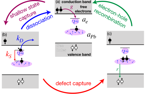
In 1978 an advance occurred when Kaplan, Solomon, and Mott (KSM) produced a new model not based on spin polarization Kaplan (1978). This KSM model posited that spins underwent an intermediary phase before recombination. Once the pair enters this intermediary phase (which might be an exciton or a donor-acceptor pair), the pair components are exclusive to one another; the pair has the option to either recombine or dissociate. The recombination process is spin-dependent while dissociation is not. Only after dissociation can either component interact, and possibly recombine, with other carriers. The KSM model explained many of the difficulties that confronted the Lepine model. Further adaptation was provided by Rong et al. where the intermediate state was supposed to be either an excited state of the defect or a shallow donor state near the conduction band.Rong et al. (1991) The carrier is first trapped into this excited state where it then has some probability of either dissociating back into an itinerant state or falling down into the ground state of the defect. It is this last process which is spin-dependent due to the Pauli exclusion principle since the defect is initially paramagnetic. The singlet ground state of the charged defect may capture and recombine with a hole and the process repeats with the defect becoming paramagnetic once more.Spaeth and Overhoff (2003) These processes are depicted in Figure 2.
In this article we use the idea of exclusive spin pairs to model both EDMR and NZFMR. Our approach utilizes stochastic Liouville equations for a spin density matrix which allows for a more general treatment than either the theories of KSM or Rong provided in the past. Previous theories of EDMR have been limited in scope by treating only transitions induced by different -factors or semiclassical nuclear fields.Glenn et al. (2013a, b); Limes et al. (2013) When examining NZFMR in systems with very few nuclear spin, it is imperative to include fully quantum hyperfine interactions. In the article we analyze NZFMR and EDMR by treating both quantum and semi-classical hyperfine interactions and then discuss the appropriate approach to use for our Si/SiO2 MOSFET devices. In the next section we alter the conventional model of trap-assisted recombination to include the ideas of pair exclusivity from KSM and the spin dependence of carrier trapping at a deep level paramagnetic defect site.
III Spin-Dependent Recombination Current
Recombination current in a semiconductor device can be explained utilizing the Shockley-Read-Hall model of recombination. In this model, electron-hole pair recombination most effectively takes place at deep level defect centers near mid-bandgap.Shockley and Read (1952); Hall (1952) Thus, in measurements of interface recombination utilizing a gated diode measurement, the recombination defect centers have energy levels very near the middle of the Si bandgap. Recombination current results from capture of both types of charge carriers at a deep level. Consider the simple case of an electron traveling through the conduction band. When the electron encounters a deep level defect, it may fall into the deep level granted that spin selection rules are obeyed. Once the electron capture takes place, the electron is available for recombination with a hole in the valence band. This process may also take place via hole capture and subsequent recombination with a conduction band electron. In the gated diode measurement, the recombination current measured through the body contact of the MOSFET has a peak which corresponds to the situation where both electron and hole densities are equal. When this occurs the recombination is maximized.
The peak of recombination current can be thought of quantitatively as follows. Under conditions where the MOSFET’s source and drain are shorted together under a forward bias with gate voltage set to yield maximum interfacial trap recombination current (see Fig. 3 which is configuration of experiment used here), the recombination current is
| (1) |
where is the equal electron and hole capture cross sections by the defect, is the thermal velocity of the carriers, is the intrinsic carrier concentration, is the areal concentration of interface traps per energy, is the gate area, is the electronic charge, is the forward bias voltage, is Boltzmann’s constant, and is the absolute temperature. This is derived independent of spin.Fitzgerald and Grove (1968) In the experiments conducted here (to be discussed further in Section VII), under forward bias holes of concentration are injected into the channel. If , then for room temperature Si is about 1.5 cm-3, and with forward bias, which gives a range of carriers between about 2 cm-3 and 7 cm-3 for the range of forward biases used here.
Equation (1) is insufficient for a few reasons: the electron and hole cross sections, and , are unequalGarrett and Brattain (1956); the recombination is mediated by an intermediate shallow state; the capture of an electron by the deep trap is spin dependent. Equation (1) can be modified to include these additional effects as described next.
III.1 Calculation for maximum spin-dependent recombination current
The maximum recombination current is
| (2) |
where is the gate area so has units of inverse time and area. The current is maximum when the gate bias is tuned in a way that there are equal numbers of electrons and holes at the interface which maximizes .
The spin-dependent capture of a carrier electron by a deep trap is a two step process: (1) the carrier electron is first weakly localized by a shallow state in the vicinity of the defect. At room temperature this state is most likely an excited state of the defect which may be near the conduction band.Rong et al. (1991); Boehme and Lips (2004); Friedrich, Boehme, and Lips (2005); Hori and Ono (2019) We assume this going forward. (2) the electron in the now charged excited state of the deep paramagnetic trap reduces to its charged ground state if the singlet condition for the spin pair is met. The theory of Shockley, ReadShockley and Read (1952), and HallHall (1952) can be modified to include the two-step capture (into the ground state) by the trap. The rate of capture of a conduction electron into the trap ground state is where we call the capture parameter (with dimension rate volume) and is the density of traps. If the two steps are each accomplished with respective capture parameters and then the total capture parameter of a conduction electron into the deep level trap by way of its excited state is
| (3) |
The last approximation is made since the transition rate to the trap ground state (large energy difference) is much smaller than the capture of a conduction electron by the excited state (small energy difference). The capture rate per volume accounts for the concentration of conduction electrons, , and is
| (4) |
where is the non-equilibrium occupancy factor at the trap level which can be determined in the steady state.Shockley and Read (1952); Hall (1952) The calculation can then proceed in a straightforward manner, following that of Shockley, ReadShockley and Read (1952), HallHall (1952), Fitzgerald and GroveFitzgerald and Grove (1968). These calculations assume that traps have constant density throughout gap but the recombination process is dominated by traps near the center. 111The calculation can also be done with a single defect level at mid gap. The purpose here is to mimic the Fitzgerald and Grove model since that is the one that gets quoted most often in the literature.
The recombination rate per unit area is:
| (5) |
where is the energy of the recombination center and is the areal density per energy of such centers. The quantities and have dimensions of inverse volume. As mentioned earlier, the deep defects possess the relevant capture parameter which, unlike for holes, should not be expressed as because the electron is already situated at the defect. Since relaxation of the excited electron spin into the ground state of the defect is spin dependent, where is the maximum possible capture parameter and is the probability of a singlet that comes from the stochastic Liouville equation which is demonstrated in the next section.
This integral in Eq. (5) can be determined to be approximately222The intrinsic Fermi level, , is assumed to be at mid gap such that and
| (6) |
with
| (7) |
The function decays monotonically from a maximum value of . Thus maximizing the recombination rate entails minimizing the quantity . Given that is the intrinsic carrier density, the only way to do so is by minimizing both and . Just as for Fitzgerald and Grove, the minimum values for these two are which can be reached by tuning the gate voltage. Note that the unequal cross sections do not change this criterion.
Substituting in these constraints on the electron and hole densities yields
| (8) |
In the limit of large forward bias, the result simplifies to
| (9) |
The argument of arccosh is large and so can be expanded as where only the last term is appreciable under physical conditions. This finally yields
| (10) |
An effective cross-section can be defined as:
| (11) |
such that
| (12) |
In the case of equal capture rates (),
| (13) |
which is exactly the result of Fitzgerald and Grove.
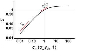
III.2 The effective recombination cross section
The spin dependence of the recombination enters through the effective cross section, , in Eq. 11. Fig. 4 plots effective cross section versus electron capture rate per area of the trap. For small compared to , the dependence is linear. We can think about it in this way: when the holes are very rapidly captured, electron capture is the limiting step so any increase in recombination requires quicker electron capture. The singlet probability, , enters within .
This calculation assumes the cross sections or capture parameters are independent of energy. There are interpretations of the cross section that might suggest that assumption to be incorrect.Ryan et al. (2015) The calculation would obviously be more difficult and probably not allow for any analytic solution.
Our system of a Pb0 defect at the Si/SiO2 interface is clearly in the regime of since the trap will be negatively charged when capturing a hole but neutral when capturing an electron. So our final expression for the maximum recombination current is
| (14) |
This expression is valid even when a magnetic field is incuded (through the parameter – see next section) as long as the bias condition for maximum current is unchanged by the magnetic field. The optimum current position has not been systematically studied in relation to magnetic field but one study shows very little change in the bias condition. Campbell et al. (2007) Therefore Eq. (14) applies for the NZFMR and EDMR experiments described in this article.
All other quantities in are considered to be spin or magnetic field-independent; hence is the normalized current at a given forward bias.
IV The Stochastic Louiville Equation and the Lyapunov Equation
We use a spin-density matrix which fully accounts for not only the spin-pair but also any number of nuclear spins. The evolution of the spin pair plus any number of relevant nuclei is governed by the stochatic Liouville equation:
| (15) |
where we use SI units and the Hamiltonians are presented in detail in the next section. The first term on the right-hand side is the Liouville or Neumann equation for the density matrix, describing the coherent evolution of the density matrix. The second and third terms signify the random processes of spin capture and spin dissociation of the spin pairs which in general may depend on their spin configuration (singlet or triplet combination occur at rates and , respectively). Assuming small spin-orbit interactions, we take ; triplets are not captured by the deep defect. The rate of singlet capture depends on the occupation of states so is written as . A rate describes the dissociation of the spin pair.
Consider the steady state which yields the following adaptation to Eq. 15:
| (16) |
with
| (17) |
This type of type of equation is known as a Lyapunov equation. can also be written as an effective Hamiltonian . The solution for the Lyapunov equation is then
| (18) |
where
| (19) |
Another relation is obtained by taking the trace of Eq. 15 in the steady state:
| (20) |
which leads to
| (21) |
The first term is the fractional yield of captured singlet pairs (creating the defect state); the second term is the fractional yield of dissociated spin pairs. Another way to write this is
| (22) |
which is combined with Eq.18 to ascertain
| (23) |
Spin relaxation and decoherence are ignored in Eq. (23).
The solution to the SLE gives
| (24) |
where is the spin degeneracy factor ( where is number of spins included in the density matrix; is also the dimension of the density matrix here). is the remaining portion of the density matrix. is the rate that which spin pairs are generated. So this factor depends on the e-h recombination and the capture of an electron by the shallow state. If we assume that e-h recombination occurs rapidly after the defect becomes , then the rate is limited by the shallow state’s capture of electrons. Therefore we write where is the capture cross section of the shallow state (assumed to be excited level of the trap), is the thermal velocity of conduction electrons, and is the density of traps.
V Interactions
V.1 Hyperfine Interaction at Defect
We ignore differences and anisotropies in carrier or defect g-factors by assuming that the radio or microwave frequency is small enough such that large static magnetic fields are unnecessary to probe the EDMR dynamics. We start by assuming only one of the two non-nuclear spins is interacting with any number of nuclear spins:
| (25) | |||
| (26) | |||
| (27) |
The first Hamiltonian is the static Zeeman interaction for the electrons and nuclei. The second Hamiltonian is the hyperfine interaction, and the third Hamiltonian is the interaction of the spins with the transverse oscillating field. After making the assumption that , the time-dependent Hamiltonian can be decomposed into two pieces :
| (28) |
and
| (29) |
The rotating wave approximation (RWA) leads to dropping (the details are described in the Appendix):
| (30) |
where we do need to assume that the hyperfine interactions have the same principle axes and possess axial symmetry. The Liouville equation becomes
| (31) |
where is the density matrix in the rotating reference frame. It is important to note that the Hamiltonians in the rotating frame are time independent.
V.2 Hyperfine Interactions at Both Electron Spins
The derivation carried out in the previous section can be repeated exactly when there is also a hyperfine interaction at . The total hyperfine interaction is then:
| (32) |
in the rotating wave approximation with the same aforementioned restrictions on both hyperfine interactions.
V.3 The Semiclassical Approximation
In the limit of a large number of nuclear spins composing the hyperfine interactions at either or both of the sites for and , the quantum mechanical nuclear spin operator is replaced by a classical vector which physically corresponds to an ensemble of nuclear moments interacting with the single electron spin Flory (1969); Schulten and Wolynes (1978); Rodgers (2007):
| (33) |
where the probability distribution functions for the nuclear fields pointing at random angles are
| (34) | |||
| (35) |
with effective hyperfine fields and with and being the spin quantum numbers for each of the nuclei at site one and site two, respectively. For simplicity, we have assumed the semiclassical distribution of fields to be isotropic (i.e. has same root mean square field as ).
Unfortunately, the transformation of the semiclassical hyperfine Hamiltonian to the rotating frame does not yield a Hamiltonian independent of time. Of course, this is inconsequential for NZFMR as we calculate with no RF field.
If one makes the secular approximation to the hyperfine interaction (which is valid for large field), then the rotating wave approximation can be used to obtain
| (36) | |||
| (37) | |||
| (38) |
So EDMR and NZFMR calculations can still be satisfactorily carried out as long as (use secular approximation) or (no RF field at all).
VI Hyperfine MC Line Shape Structure
VI.1 Quantum Mechanical Nuclear Spins
The recombination currents, either with or without the oscillating field, are guaranteed to have the same value only for large magnetic fields (i.e. far from resonances and near zero field transitions); it is convenient then to use as a figure of merit. The most sensitive experiments determine a spin-dependent recombination current which will be proportional to which is the quantity we call “NZFMR” or “EDMR”. Figure 5 shows two representative calculations using different rates and with an isotropic hyperfine interaction at one (a,b) or both (c,d) of the sites.
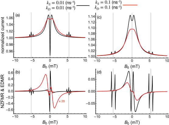
The EDMR is nearly absent when the spin kinetics are increased (red) since the spins are either combining or dissociating before the resonant transition can take place. Similarly, the increased rates also cause an overall broadening and reduction in magnitude of the curve.
Note that in panels (a,c), the NZFMR line shape consists of a broad feature (‘shoulder’) and a narrow feature (‘dimple’). The ‘dimple’ appears more pronounced in the response derivative (b,d). The ‘shoulder’ is barely observable in the black curve of (b) while the red curve’s ‘dimple’ in (b) is weaker than the ‘shoulder’. The black ‘shoulder’, ‘dimple’, and EDMR are comparable in (c) though reducing the ‘dimple’ (by appropriate choice of parameters) tends to also result in a reduction of the EDMR as shown by the red curve. The ‘dimple’ appears in fields less than and are similar to what has been observed in the spin chemistry of radical pair reactions (low-field effect or LFE) and the magnetic field effects studied in organic spintronics. The origin is subtle and qualitatively ascribed to the conservation of angular momentum Brocklehurst and McLauchlan (1996). Consider initial singlet spin pair states with a spin- nucleus located at one of the two spins. In zero applied field both and are conserved where . The conservation of these quantities restricts the overall hyperfine-induced transitions between singlet and triplet states. When a small field is applied (along ) only is conserved. As a result the spin evolution is given more freedom when this small field is applied and more triplets may be formed at the expense of the singlet population. As the field increases, eventually energetics play a role and the non-zero states separate out from the states which gives rise to fewer transitions out of the singlet state and an eventual saturation of the singlet population.
We observe here, and we find this to be true in general, that the ‘dimple’ originating from the LFE is typically smaller in size when hyperfine interactions exist at both sites.
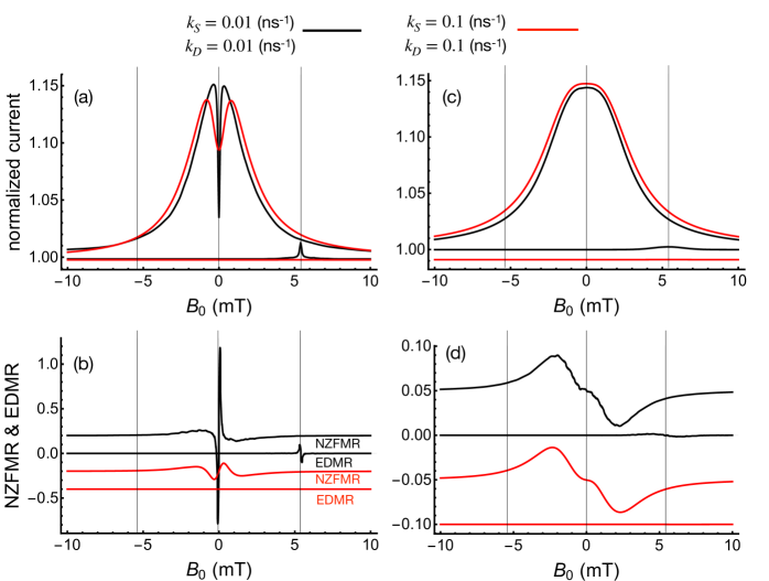
VI.2 Semiclassical Nuclear Spins
Figure 6 graphs examples of NZFMR and EDMR when one or both spins interact with a large number of nuclear spins, justifying the semiclassical approximation for the hyperfine interaction. Of particular interest is (c,d) where both spins are in the classical hyperfine field. The low-field effect is significantly reduced compared to (a,b). Figure 6 uses identical hyperfine couplings for the two electrons or holes but this is not expected to be physical since the two states are different. Again we find that the LFE is typically smaller in size (relative to the ‘wide shoulder’ or WS) when hyperfine interactions exist at both sites.
To clarify what is meant by the semiclassical approximation – not every defect spin will be in same nuclear environment since 29Si is only present for about 4.7 % of the silicon atoms present. 4.7 % of the defects will have a nuclear spin at their host site but a great many more will have nuclear spins in their vicinity and still interact with the nuclear spin. If the 12 nearest silicon atoms to the central defect are considered, there are 224 possible configurations (i.e. ranging from zero 29Si to 13 29Si); nearly half of those configurations possess at least one spinful nucleus.While the hyperfine interaction is strongest if the Pb defect itself is 29Si, it is much more likely that a Pb defect will experience a smaller hyperfine interaction from a next nearest neighboring 29Si nucleus and it is this higher likelihood that can dominate the response.333See Appendix for details on these probabilities. Our semiclassical calculation ascribes an effective hyperfine constant to describe the entire ensemble of defects in their various 29Si (and hydrogen) arrangements.444We are making this argument based on the easier-to-visualize (111) surface; it is expected to hold true also for the (100) surface which is the surface in our experiments.
VI.3 NZFMR and EDMR in Si/SiO2 MOSFETs
By comparing to measurements of spin-dependent recombination current at Si/SiO2 interfaces in the remainder of this article, we find that the semi-classical approximation does a much better job of explaining the NZFMR and EDMR line shape features simultaneously.
VII Experiment
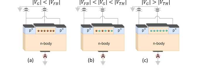
Our experiments utilized a low field and frequency (5.4 mT and 151 MHz at resonance) custom-built spectrometer consisting of a Kepco BOP 50-2M bipolar power supply, a Lakeshore Cryogenics model 475 DSP Gaussmeter and temperature compensated Hall probe, a Agilent model 83732B synthesized signal generator, a Doty Scientific RF coil and 150 MHz tuning box, and a custom-built electromagnet with a separate pair of coils for magnetic field modulation. We utilize a Stanford Research Systems SR570 preamplifier for transimpedance amplification of the sample device current. We utilize LabVIEW software for magnetic field modulation, spectrometer control, and data acquisition and processing. Noise limits the feasibility of the measurement since the spin-dependent changes in device current are a very small fraction of the total current. Thus, the LabVIEW software also utilizes a virtual lock-in amplifier with frequency and phase sensitive detection of the magnetic field modulated device current. The resulting EDMR and NZFMR curves appear as approximate derivatives of the true spectra. All measurements were made at room temperature. The planar Si/SiO2 MOSFET has a 7.5 nm thick SiO2 gate dielectric with 41,000 m2 channel area and a shorted source and drain region.The gate of the total structure is comprised of 420 fingers each with a length of 1 m and a width of 98 m and a shorted source and drain region.
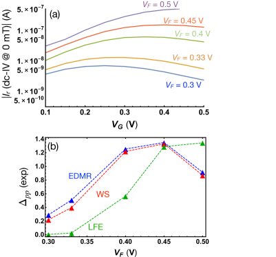
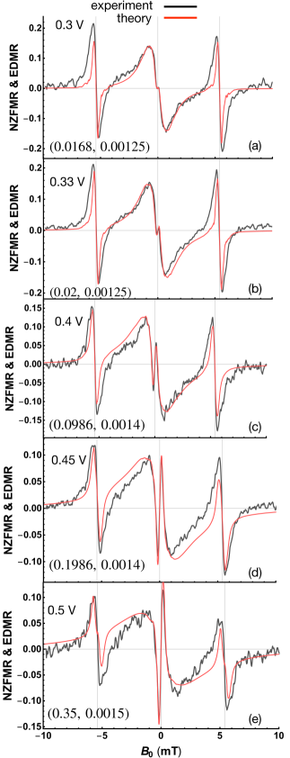
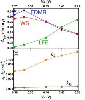
The oxidation was then followed up by a N2 anneal at 925∘C. The devices were irradiated under a 0.2 V gate bias with a dose of 1 MRad. For our EDMR and NZFMR measurements, the source/drain to body junction biased at 0.3V, 0.33V, 0.4V, 0.45V, and 0.5V. with the gate bias held corresponding to the peak in the body current (Fig. 7(a)), with the body grounded; this biasing condition corresponds to the peak recombination current and optimal signal-to-noise. This biasing scheme is dc-IV and was first introduced by Grove.Grove (1967) The recombination peak corresponds to the condition when electron and hole densities at the interface are equal. This condition is satisfied with the surface potential in depletion corresponding to .
The light red curves in Fig. 8 shows the post-irradiation spectrum. The pre-irradiation spectrum (not shown) exhibits neither an NZFMR or EDMR response. X-band measurements at 9.4 GHz were also made on the same irradiated Si/SiO2 MOSFETs, indicating that the near-interface traps are dominated by the Pb center.Jupina and Lenahan (1990) Fig. 7(b) shows the peak-to-peak amplitudes of all three features seen in the experiment: EDMR occurring near mT, WS (wide shoulder), the broader shape (‘shoulder’) around zero field, and the LFE, the narrower feature (‘dimple’) around zero field. Note that, for the sake of comparing features to the theory, Fig. 8 does not display the actual values of the experimental amplitudes found in Fig. 7(b).
VIII Discussion
To offer an explanation of the experimental results of Fig. 8, we first examine the lower forward biases of Fig. 8 (a) and (b). Fig. 8 (b) was considered in Ref. Harmon et al., 2020. We find that using the quantum model, neither one nor two site hyperfine interactions can satisfactorily explain the NZFMR and EDMR simultaneously. For instance, an excellent fit to the NZFMR yields a minuscule EDMR peak. However by assuming semiclassical hyperfine interactions at both sites, NZFMR and EDMR relative features observed in our experiments can be satisfactorily recreated (red curves in Fig. 8 ). The absolute amplitudes of the experimental traces in Fig. 8 have been adjusted in order to compare the experimental and theoretical shapes. Figure 7 (b) plots the actual experimental peak-to-peak measured values. The theory curves in Fig. 8 are no longer normalized by the singlet probability at large field. Figure 9 (a) plots the EDMR, WS, and LFE peak-to-peak amplitude extracted from Fig. 8. Figure 9 (b) displays the trends in and there were found when fitting the model to the measurements.
The semiclassical model for the defect spin is certainly sensible since each defect has a high likelihood of experiencing several Si hyperfine interactions. Moreover there is an abundance of nuclear spins originating from the passivating hydrogen at the surface for whose hyperfine couplings we do not possess detailed information.Himspel et al. (1988); Brower (1988); Tuttle (1999) Given the range of hyperfine interactions from silicon (see Table I), the width of one half a milliTesla is not surprising. The carrier spin also experiences a semiclassical interaction – this is more apparent since the weakly bound electron will sample a larger number of nuclei within its localization radius. For the same reason, any hyperfine interaction felt would be expected to be less than that of the defect spin due to the less localized nature of the state. In light of the data that has been shown so far here, many hyperfine interactions at both spins, appears as the most likely possibility to explain both the NZFMR and EDMR relative line shape structure.
Recently, a paper by Frantz et al. analyzed spin dependent recombination NZFMR curves alone for the Si/SiO2 MOSFET and spin-dependent trap assisted tunneling leakage current across the insulator in a hydrogenated amorphous silicon MIS capacitor.Frantz et al. (2020) By using the quantum model for the hyperfine interaction, accurate parameters for the hyperfine interactions and relative hyperfine abundances were extracted from a nonlinear least squares fitting routine. For the same set of parameters obtained from the fit for Si/SiO2, the EDMR was negligible in size which is the same conclusion reached here.
This discrepancy can be explained by the following considerations that should be borne out by future in-depth analysis of the two approaches. While NZFMR and EDMR originate from same spin-dependent processes, their mechanics are different such that their dependencies on the various rates are not expected to be the same. A primary distinction is that EDMR requires an alternating field of magnitude to induce spin transitions while NZFMR does not. In the semiclassical model used here, the values for and were at least an order of magnitude smaller than the values found by Frantz et al. using purely quantum nuclear spins when fitting the NZFMR line shape. As seen in Figs. 5 and 6, smaller and increase the relative size of EDMR in both the quantum and semiclassical calculations. The results here and those of Frantz et al. suggest that the rates and are not constant but are drawn from a distribution of values.
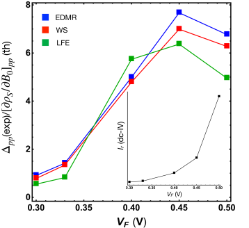
IX Analysis of Forward Bias Dependence
The experimental line shape features are quantified by their peak-to-peak amplitudes, . These amplitudes as a function of forward bias are shown in Figure 7 (b). is related to the maximum recombination current by where is an unknown function of forward bias. We expect to scale in size with the dc-IV recombination current. This is tested in Fig. 10 by plotting the ratio
| (39) |
which should yield . The main lines and inset line both increase with forward bias except at the largest forward bias; however in view of Fig. 7(b), there is uncertainty whether the maximum dc-IV recombination current was achieved at 0.5 V. Without knowing the precise dependence of the field modulated device current on dc-IV, a more rigorous analysis of the relationship between the model and the experiment is not possible.
X Conclusion
The goal of this article has been to provide a sound theoretical basis for the near-zero-field magnetoresistance phenomena present at oxide-semiconductor interfaces in technologically relevant devices. The focus has been on spin-dependent recombination. We expect the theoretical approach to apply for spin-dependent trap-assisted transport (SDTAT) where NZFMR is also observed.Frantz et al. (2020). The model presented is able to qualitatively explain a series of spin-dependent recombination experiments where the gate and forward biases were changed. To do so we demonstrated how a quantum model for the hyperfine interaction was insufficient to simultaneously describe the NZFMR and EDMR responses. Instead we utilized a semiclassical approximation for the hyperfine interaction which is reasonable considering the abundance of nuclear spins near the relevant spin pair.
XI Acknowledgements
The project or effort depicted was or is sponsored by the Department of the Defense, Defense Threat Reduction Agency under Grant HDTRA 1-18-1-0012 and Grant 1-16-0008. The content of the information does not necessarily reflect the position or the policy of the federal government, and no official endorsement should be inferred.
XII Data Availability
The data that support the findings of this study are available from the corresponding author upon reasonable request.
References
- Wertz (1970) J. Wertz, Electron Spin Resonance: Elementary Theory and Practical Applications (Springer, 1970).
- (2) W. M. Chen, in EPR of Free Radicals in Solids. Progress in Theoretical Chemistry and Physics, Vol. 10, edited by A. Lund and M. Shiotani.
- Boehme and Lips (2006) C. Boehme and K. Lips, “The investigation of charge carrier recombination and hopping transport with pulsed electrically detected magnetic resonance techniques,” in Charge Transport in Disordered Solids with Applications in Electronics (John Wiley & Sons, Ltd, 2006) Chap. 5, pp. 179–219, https://onlinelibrary.wiley.com/doi/pdf/10.1002/0470095067.ch5 .
- Lenahan and Conley Jr. (1998) P. M. Lenahan and J. F. Conley Jr., “What can electron paramagnetic resonance tell us about,” J. Vac. Sci. Technol. B 16, 2134–2153 (1998).
- Watkins (1999) G. Watkins, “Epr of defects in semiconductors: Past, present, future,” Physics of the Solid State 41, 746–750 (1999).
- Nishi (1971) Y. Nishi, Jpn. J. Appl. Phys. 10, 52 (1971).
- Nishi, Tanaka, and Ohwada (1972) Y. Nishi, T. Tanaka, and A. Ohwada, Jpn. J. Appl. Phys. 11, 85 (1972).
- Lenahan and Dressendorfer (1982) P. M. Lenahan and P. V. Dressendorfer, Appl. Phys. Lett. 41, 542 (1982).
- Lenahan and Dressendorfer (1984) P. M. Lenahan and P. V. Dressendorfer, J. Appl. Phys. 55, 3495 (1984).
- Kim and Lenahan (1988) Y. Y. Kim and P. M. Lenahan, Appl. Phys. Lett. 64, 3551 (1988).
- Vranch, Henderson, and Pepper (1988) L. Vranch, B. Henderson, and M. Pepper, Appl. Phys. Lett. 52, 1161 (1988).
- Miki et al. (1988) H. Miki, M. Noguchi, K. Yokogawa, B. Kim, K. Asada, and T. Suganor, IEEE Trans. Electron Devices 35, 2245 (1988).
- Awazu, Watanabe, and Kawazoe (1993) K. Awazu, W. Watanabe, and H. Kawazoe, Appl. Phys. Lett. 73, 8519 (1993).
- Ashton et al. (2019) J. P. Ashton, S. J. Moxim, P. M. Lenahan, C. G. Mckay, R. J. Waskiewicz, K. J. Myers, M. E. Flatt , N. J. Harmon, and C. D. Young, “A new analytical tool for the study of radiation effects in 3-d integrated circuits: Near-zero field magnetoresistance spectroscopy,” IEEE Transactions on Nuclear Science 66, 428–436 (2019).
- (15) S. T. P. D. M. Fleetwood and R. D. Schrimpf, in Defects in Microelectronic Materials and Devices, Vol. 10, edited by S. T. P. D. M. Fleetwood and R. D. Schrimpf.
- Eaton et al. (2010) G. R. Eaton, S. S. Eaton, D. P. Barr, and R. T. Weber, Quantitative EPR (Springer, 2010).
- J.T. Krick and W.Weber (1991) P. M. L. J.T. Krick and W.Weber, Appl. Phys. Lett. 59, 3437 (1991).
- Campbell et al. (2007) J. P. Campbell, P. M. Lenahan, C. J. Cochrane, A. T. Krishnan, and S. Krishnan, “Atomic-scale defects involved in the negative-bias temperature instability,” IEEE Transactions on Device and Materials Reliability 7, 540–557 (2007).
- J.W. Gabrys (1993) W. W. J.W. Gabrys, P.M. Lenahan, Microelectronics Engineering 22, 273 (1993).
- Cochrane and Lenahan (2012) C. J. Cochrane and P. M. Lenahan, “Zero-field detection of spin dependent recombination with direct observation of electron nuclear hyperfine interactions in the absence of an oscillating electromagnetic field,” J. Appl. Phys. 112, 123714 (2012).
- Cochrane and Lenahan (2013) C. J. Cochrane and P. M. Lenahan, “Detection of interfacial Pbcenters in Si/SiO2metal-oxide-semiconducting field-effect transistors via zero-field spin dependent recombination with observation of precursor pair spin-spin interactions,” Applied Physics Letters 103 (2013), 10.1063/1.4817264.
- Harmon et al. (2020) N. J. Harmon, S. R. McMillan, J. P. Ashton, P. M. Lenahan, and M. E. Flatt , “Modeling of near zero-field magnetoresistance and electrically detected magnetic resonance in irradiated si/sio2 mosfets,” IEEE Transactions on Nuclear Science , 1–1 (2020).
- Mott (1987) N. F. Mott, Conduction in non-crystalline materials (Oxford, New York, 1987).
- Anders et al. (2018) M. A. Anders, P. M. Lenahan, C. J. Cochrane, and J. van Tol, “Physical nature of electrically detected magnetic resonance through spin dependent trap assisted tunneling in insulators,” Journal of Applied Physics 124, 215105 (2018), https://doi.org/10.1063/1.5057354 .
- Mermer et al. (2005) O. Mermer, G. Veeraraghavan, T. L. Francis, Y. Sheng, D. T. Nguyen, M. Wohlgenannt, A. Köhler, M. K. Al-Suti, and M. S. Khan, “Large magnetoresistance in nonmagnetic -conjugated semiconductor thin film devices,” Phys. Rev. B 72, 205202 (2005).
- Prigodin et al. (2006) V. N. Prigodin, J. D. Bergeson, D. M. Lincoln, and A. J. Epstein, “Anomalous room temperature magnetoresistance in organic semiconductor,” Synthetic Metals 156, 757–761 (2006).
- Maciá et al. (2014) F. Maciá, F. Wang, N. J. Harmon, M. Wohlgenannt, A. D. Kent, and M. E. Flatté, “Organic magnetoelectroluminescence for room temperature transduction between magnetic and optical information,” Nature Communications 5, 3069 (2014).
- Wang, Li, and Zou (2017) Y.-M. Wang, J.-G. Li, and J. Zou, “Detecting the presence of a magnetic field under Gaussian and non-Gaussian noise by adaptive measurement,” Physics Letters A 381, 1866–1873 (2017).
- Shockley and Read (1952) W. Shockley and W. T. Read, “Statistics of the Recombination of Holes and Electrons,” Physical Review 87, 835–842 (1952).
- Hall (1952) R. N. Hall, “Electron-hole recombination in germanium,” Phys. Rev. 87, 387–387 (1952).
- Lepine and Prejean (1972) D. J. Lepine and J. J. Prejean, Proceedings of the 10th International Conference on the Physics of Semiconductors , 805 (1972).
- Lepine (1972) D. J. Lepine, Phys. Rev. B 6, 436 (1972).
- L’vov (1977) T. D. V. K. I. A. L’vov, V. S., Sov. Phys. Semicond. 11, 661 (1977).
- Wosinski (1977) F. T. Wosinski, W., Phys. Status Solidi B. 83, 93 (1977).
- Mendz (1980) H. D. Mendz, G., J. Phys. C 13, 6737 (1980).
- Kaplan (1978) S. I. M. N. F. Kaplan, D., J. Phys (Paris) 39, L51 (1978).
- Rong et al. (1991) F. Rong, W. Buchwald, E. Poindexter, W. Warren, and D. Keeble, “Spin-dependent shockley-read recombination of electrons and holes in indirect-band-gap semiconductor p-n junction diodes,” Solid-State Electronics 34, 835 – 841 (1991).
- Spaeth and Overhoff (2003) J. M. Spaeth and H. Overhoff, Point Defects in Semiconductors and Insulators: Determination of Atomic and Electronic Structure from Paramagnetic Hyperfine Interactions (Springer, 2003).
- Glenn et al. (2013a) R. Glenn, W. J. Baker, C. Boehme, and M. E. Raikh, “Analytical description of spin-Rabi oscillation controlled electronic transitions rates between weakly coupled pairs of paramagnetic states with S=1/2,” Physical Review B 87, 155208 (2013a).
- Glenn et al. (2013b) R. Glenn, M. E. Limes, B. Saam, C. Boehme, and M. E. Raikh, “Analytical study of spin-dependent transition rates within pairs of dipolar and strongly exchange during magnetic resonant excitation coupled spins with s = 1,” Phys Rev B 165205, 1–9 (2013b).
- Limes et al. (2013) M. E. Limes, J. Wang, W. J. Baker, B. Saam, and C. Boehme, “Numerical study of spin-dependent transition rates within pairs of dipolar and exchange coupled during magnetic resonant excitation spins with s = 1,” Phys. Rev. B 165204, 17–22 (2013).
- Fitzgerald and Grove (1968) J. Fitzgerald and A. S. Grove, “Surface recombination in semiconductors,” Surface Science 9, 347–369 (1968).
- Garrett and Brattain (1956) C. G. Garrett and W. H. Brattain, “Distribution and Cross?Sections of Fast States on Germanium Surfaces,” Bell System Technical Journal 35, 1041–1058 (1956).
- Boehme and Lips (2004) C. Boehme and K. Lips, “A pulsed EDMR study of hydrogenated microcrystalline silicon at low temperatures,” Physica Status Solidi (C) 1, 1255–1274 (2004).
- Friedrich, Boehme, and Lips (2005) F. Friedrich, C. Boehme, and K. Lips, “Triplet recombination at P b centers and its implications for capture cross sections,” Journal of Applied Physics 97, 5–8 (2005).
- Hori and Ono (2019) M. Hori and Y. Ono, “Charge Pumping under Spin Resonance in Si (100) Metal-Oxide-Semiconductor Transistors,” Physical Review Applied 11, 1 (2019).
- Ryan et al. (2015) J. T. Ryan, A. Matsuda, J. P. Campbell, and K. P. Cheung, “Interface-state capture cross section - Why does it vary so much?” Applied Physics Letters 106, 16–19 (2015).
- Flory (1969) P. J. Flory, Statistical Mechanics of Chain Molecules (Interscience Publishers, 1969).
- Schulten and Wolynes (1978) K. Schulten and P. G. Wolynes, “Semiclassical description of electron spin motion in radicals including the effect of electron hopping,” J. Chem. Phys. 68, 3292 (1978).
- Rodgers (2007) C. Rodgers, Magnetic Field Effects in Chemical Systems, Ph.D. thesis, University of Oxford (2007).
- Brocklehurst and McLauchlan (1996) B. Brocklehurst and K. A. McLauchlan, “Free radical mechanism for the effects of environmental electromagnetic fields on biological systems,” International Journal of Radiation Biology 69, 3–24 (1996).
- Grove (1967) A. S. Grove, “Physics and technology of semiconductor devices,” Tech. Rep. (1967).
- Jupina and Lenahan (1990) M. A. Jupina and P. M. Lenahan, “Spin dependent recombination: a /sup 29/si hyperfine study of radiation-induced p/sub b/ centers at the si/sio/sub 2/ interface,” IEEE Transactions on Nuclear Science 37, 1650–1657 (1990).
- Himspel et al. (1988) F. J. Himspel, F. R. McFeely, A. Taleb-Ibrahimi, J. A. Yarmoff, and G. Hollinger, Phys. Rev. B 38, 6084–6096 (1988).
- Brower (1988) K. L. Brower, Phys. Rev. B 38, 9657–9666 (1988).
- Tuttle (1999) B. Tuttle, Phys. Rev. B 60, 2631–2637 (1999).
- Frantz et al. (2020) E. Frantz, N. J. Harmon, S. R. McMillan, S. Moxim, M. E. Flatt , and P. M. Lenahan, “Extraction of isotropic electron-nuclear hyperfine coupling constants of paramagnetic point defects from near-zero field magnetoresistance spectra via least squares fitting to models developed from the stochastic quantum liouville equation,” submitted to J. Appl. Phys. , 1–1 (2020).
- Edwards (1987) A. H. Edwards, “Theory of the Pb center at the <111> Si/SiO2 interface,” Physical Review B 36, 9638–9648 (1987).
- Brower (1983) K. L. Brower, “29Si hyperfine structure of unpaired spins at the Si/SiO2interface,” Applied Physics Letters 43, 1111–1113 (1983).
Appendix A Derivation of the Rotating Wave Approximation Hamiltonian
When transforming to a rotating coordinate system, either or become time independent while the other term obtains a relative precession rate that is routinely dropped within the so-called rotating wave approximation.
| (40) |
where the spin operators are dimensionless and .
We can transform to a rotating coordinate system for which the transformed density matrix is with . The motivation behind this transformation is to make the Hamiltonian time-independent. The Zeeman Hamiltonians are
| (41) | |||
| (42) |
Since , the Zeeman Hamiltonians approximate as
| (43) |
For the RWA to eliminate time dependence in the hyperfine term, some restrictions on the hyperfine terms must be assumed. All hyperfine coupling tensors must have the same principle axes and possess axial symmetry (i.e. , , etc). When these conditions are satisfied,
| (44) |
The left-hand side of the Liouville equation becomes
| (45) |
and then
| (46) |
The last term we get from the transformed Liouville equation for which the coherent term can be determined from:
| (47) |
The remaining terms (stochastic ones) are determined similarly to yield a final expression:
| (48) |
The two terms on the right hand side can be combined to make an effective Hamiltonian
| (49) |
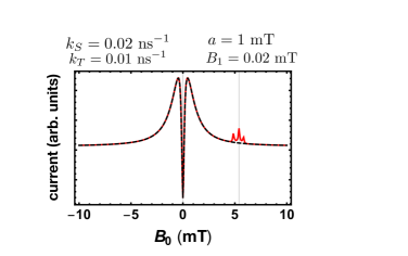
For the range of parameters occurring in this article, using the RWA does not effect the NZFMR line shape as shown in Figure 11.
Appendix B The Pb defect at the Si/SiO2 Interface
B.1 Defect-Hyperfine Statistics for Si/SiO2 dangling bond defects
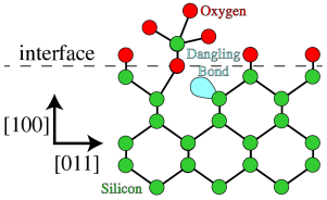
The Pb dangling bond defect at the interface of Si/SiO2 is one of the better characterized defects. Experimental and theoretical Edwards (1987) treatments have determined its hyperfine structure so make this system an excellent testbed of our theory. The defect is shown in Figure 1.
The quickest approach is to assume that the defect atom dominates the magnetic field response of the recombination current. Only 4.7% of silicons possess a spin- nucleus so to a first approximation only this subset is included. The hyperfine interaction is not isotropic as tabulated in Table 1 where the first row is the hyperfine interaction with the defect center atom. For now neighboring silicons are neglected.
Binomial probability distribution:
| (50) |
which tells you the probability for of Si atoms to be the 29Si if the probability for any individual Si is . So the probability of a specified defect being 29Si is which is 0.047 if . But we are also interested whether nearby Si atoms have spinful nuclei since the defect wave function has some spatial overlap with, as we will see, its nearest and next nearest neighbors Edwards (1987). The hyperfine interactions are equivalent with its nearest neighbors when that nearest neighbor possesses nuclear spin. Since there are three such atoms, the probability of of those three being spinful is . As for next nearest neighbors (of which there are nine), there exist two different hyperfine couplings to the paramagnetic defect spin: three atoms are termed as bulk next nearest neighbors and the other six atoms are known as surface next nearest neighbors Edwards (1987). The respective probabilities for spinful nuclei are and . The joint probability distribution for any number of the 13 relevant atoms to have spinful nuclei is
| (51) |
where , , , and . A given defect then is in one of 224 configurations — 46% of which possess at least one spinful nucleus at either the defect or its nearest/next nearest neighbors.
Furthermore, if hyperfine interactions exists for both electrons, the probability distribution must be expanded to include the probabilities of interaction at the second electron as well.
B.2 Hyperfine interactions of Pb defect
Brower was the first to measure the Pb hyperfine constants using EPR Brower (1983). The measurement took place at 20 K and showed that the interaction was anisotropic.
| (52) |
where
| (53) |
All matrix elements are listed in Table 1 as computed by Edwards in Ref. Edwards, 1987. The experiment of Brower agree well with the “Defect atom” numbers in the table.
| Number/defect | ||||||||
|---|---|---|---|---|---|---|---|---|
| Defect atom | 1 | 9.65 | 15.72 | 11.67 | -2.023 | -2.023 | 4.046 | |
| Nearest neighbor (n.n) | 3 | 0.188 | -0.211 | 0.095 | 0.116 | |||
| Bulk next n.n | 3 | 2.33 | -0.214 | -0.153 | 0.367 | |||
| Surface next n.n. | 6 | 0.229 | -0.057 | 0.015 | 0.042 |