Observation of gapped state in rare-earth monopnictide HoSb
Abstract
The rare-earth monopnictide family is attracting an intense current interest driven by its unusual extreme magnetoresistance (XMR) property and the potential presence of topologically non-trivial surface states. The experimental observation of non-trivial surface states in this family of materials are not ubiquitous. Here, using high-resolution angle-resolved photoemission spectroscopy (ARPES), magnetotransport, and parallel first-principles modeling, we examine the nature of electronic states in HoSb. Although we find the presence of bulk band gaps at the and -symmetry points of the Brillouin zone (BZ), we do not find these gaps to exhibit band inversion so that HoSb does not host a Dirac semimetal state. Our magnetotransport measurements indicate that HoSb can be characterized as a correlated nearly-complete electron-hole-compensated semimetal. Our analysis reveals that the nearly perfect electron-hole compensation could drive the appearance of non-saturating XMR effect in HoSb.
Introduction
Topological insulators (TIs) with novel properties such as extreme magnetoresistance and high carrier mobility are currently attracting intense interests in condensed matter and material science communities. A TI supports the presence of gapless topological surface states (TSSs) with Dirac-cone-like energy dispersions within an inverted gap between the bulk conduction and valence bands Hasan ; Xia ; Hasan_review_2 ; RMP . The discovery of TIs has spurred the exploration of gapless nontrivial states beyond the insulators to include a great variety of topological semimetals such as the Dirac-, Weyl-, and nodal-line/loop semimetals in which the bulk bandgap opening is prohibited by crystalline symmetries Dai ; Neupane_2 ; Suyang_Science ; Hong_Ding ; Neupane_5 . These developments have opened up exciting new routes for finding exotic quantum phases and improved materials platforms for constructing low-power electronics/spintronics devices Hasan ; Yoshomi . A distinct nontrivial state with TSSs has been recently reported in a three-dimensional (3D) material with a vanishing global bandgap Kane ; Wang where the TSSs overlap with the bulk states. The rare-earth monopnictide (REM) family is drawing special interests as a rich playground for investigating Dirac fermionic excitations. REMs have been predicted to host topological Dirac semimetal as well as 3D TI states Zeng and exhibit extremely large magnetoresistance (XMR) Pavlosuik ; Tafti ; Guo ; Zhu ; Shen ; Yu ; HoBi . Although a good deal of work in the literature concerns the linearly-dispersing states and their role in driving XMR in the REMs, a robust conclusion in this regard remains a matter of debate. Although the conventional explanation for the XMR effects involves electron-hole compensation Tafti ; Guo ; Yu ; HoBi ; DK1 ; DK2 , the observation of XMR in the REM family and numerous other topological materials such as WTe2 Mazhar , Cd3As2 Cava1 , PtSn4 Canfield , and TaAs TaAs_transport has ignited the possibility that XMR might have its origin in the forbidden backscattering channels of topological materials Cava1 ; TaAs_transport . Notably, TSSs have been reported in LaBi, LaSb, CeSb, and CeBi by various groups Felser ; Feng ; Dessau ; Niu ; Lou ; Kaminski ; Ding ; Oinuma ; Nasser ; Kondo ; Guo whereas LaAs, LuBi, YBi, YSb, and CeSb have been suggested to be topologically trivial materials Dessau ; Shen ; Tafti ; Pavlosuik ; Oinuma ; Suzuki . The presence of a Dirac semimetal state is suggested in NdSb Madhab and DySb Zhu . With this background in mind, further experimental and theoretical studies are needed to gain an understanding of the nature of Dirac-like states and how they are connected with XMR in the REM family.
Rare-earth elements with their f-electrons provide strongly-correlated, tunable magnetic ground states in the REM family. Moving from La to Lu in the lanthanide series, one observes a nonmagnetic to ferromagnetic transition. HoSb that supports an antiferromagnetic (AFM) ground state Vogt is not a well-studied member of the REM family. It displays a magnetic transition from an MnO-type AFM arrangement to a HoP-type ferromagnetic arrangement under external magnetic field Mag_trans . More recently, an unusual XMR has been reported in HoSb Xia1 ; Gupta .
Here, we report the observation of a gapped state at the point of the BZ in HoSb. Using angle-resolved photoemission spectroscopy (ARPES) along with first-principles calculations and magneto-transport measurements, we examine in-depth the electronic structures of this material. Our analysis reveals the presence of a highly anisotropic Dirac-like cone at the point. Our experimental data and theoretical results identify a small gap around 470 meV below the Fermi level. More importantly, our calculations of the 2 invariant show that HoSb assumes a trivial topological state (2 = 0). We analyze our magnetotransport results to show that the presence of nearly perfect electron-hole compensation could drive the appearance of non-saturating XMR effect in HoSb.
Results
Sample characterizations and electronic structure
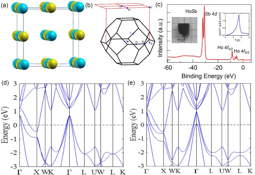
HoSb crystalizes in a rock-salt-type crystal structure with space group Fm-3m like other members of the REM family (see Fig. 1 (a)). Our X-ray diffraction measurements confirm the cubic crystal structure with the refined lattice parameter a = 6.13(1) Å. Here, yellow and blue balls correspond to the Ho and Sb atoms, respectively (Fig. 1 (a)). Figure 1 (b) shows the bulk BZ and its projection on the (001) surface. The core level spectrum is shown in Fig. 1 (c). Peaks of Sb 4d (32 eV), Ho 4f5/2 (8.6 eV) and Ho 4f3/2 (5.2 eV) are clearly resolved. The observation of sharp peaks in the spectrum indicates that our HoSb samples are of good quality. The left inset of 1(c) shows a picture of our cubic crystal. In order to determine the magnetic transition temperature, we consider the temperature derivative of resistivity, , in the low-temperature regime (see Fig. 1(c)-right inset). One can clearly see the magnetic transition at around 5.7 K, which is in accord with previous report Mag_trans .
We present the bulk band structure of HoSb without including spin-orbit coupling (SOC) effects and treating f-electrons as core orbitals in Fig. 1(d). There are three hole-like bands at the point and one electron-like band at the point that crosses the Fermi level. On including SOC in the computations, salient features of this band structure picture are preserved (Fig. 1(e)), although the third hole-band at moves closer to the Fermi level so that its top cross the Fermi level. At the point, the gap between the Ho d and Sb p states is seen to nearly close. An inspection of the valence and conduction bands shows the presence of gaps of 110 meV and 90 meV at the and points, respectively.
Fermi surface and constant-energy contour plots
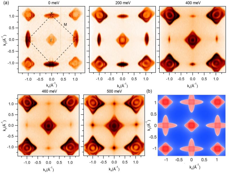
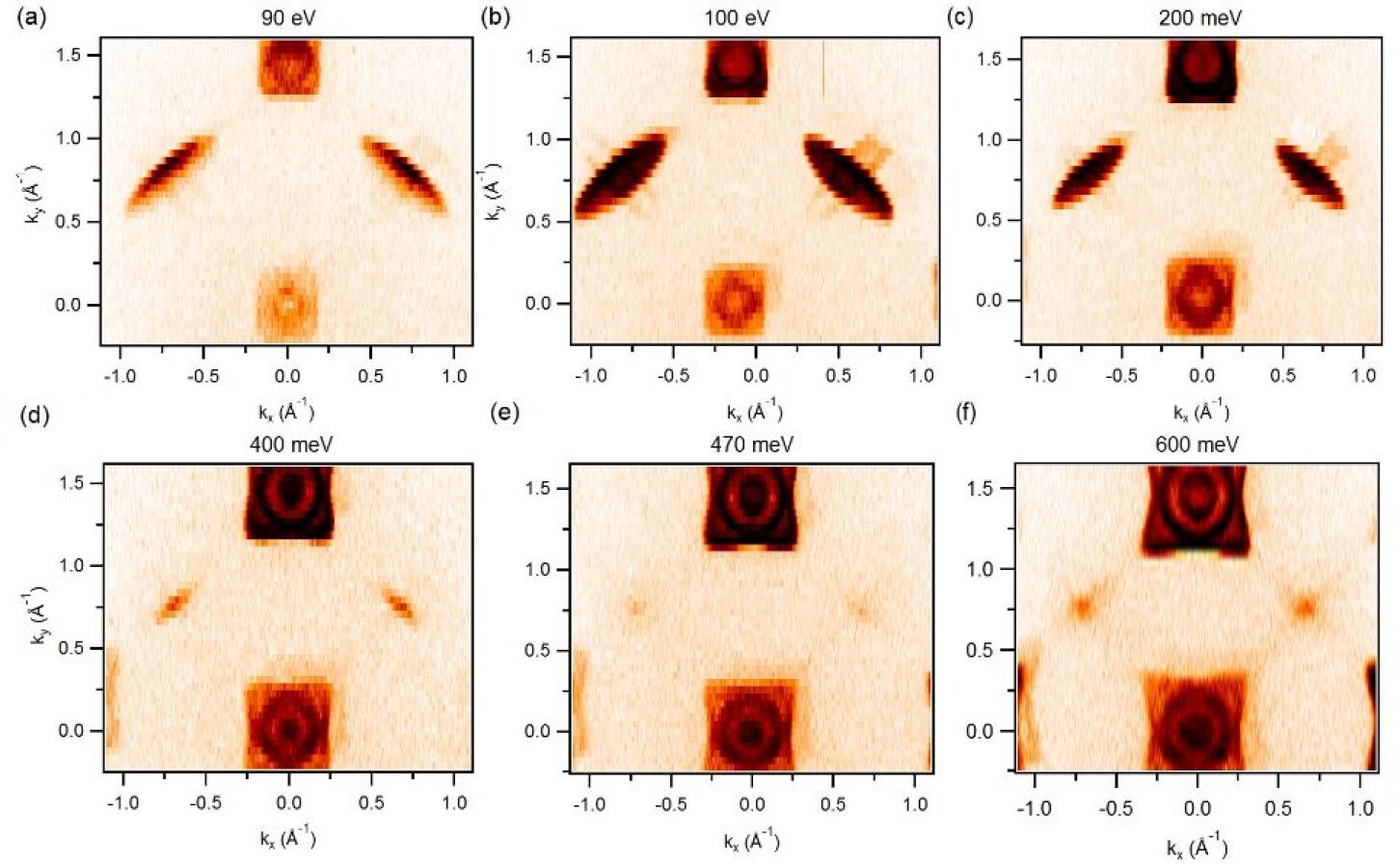
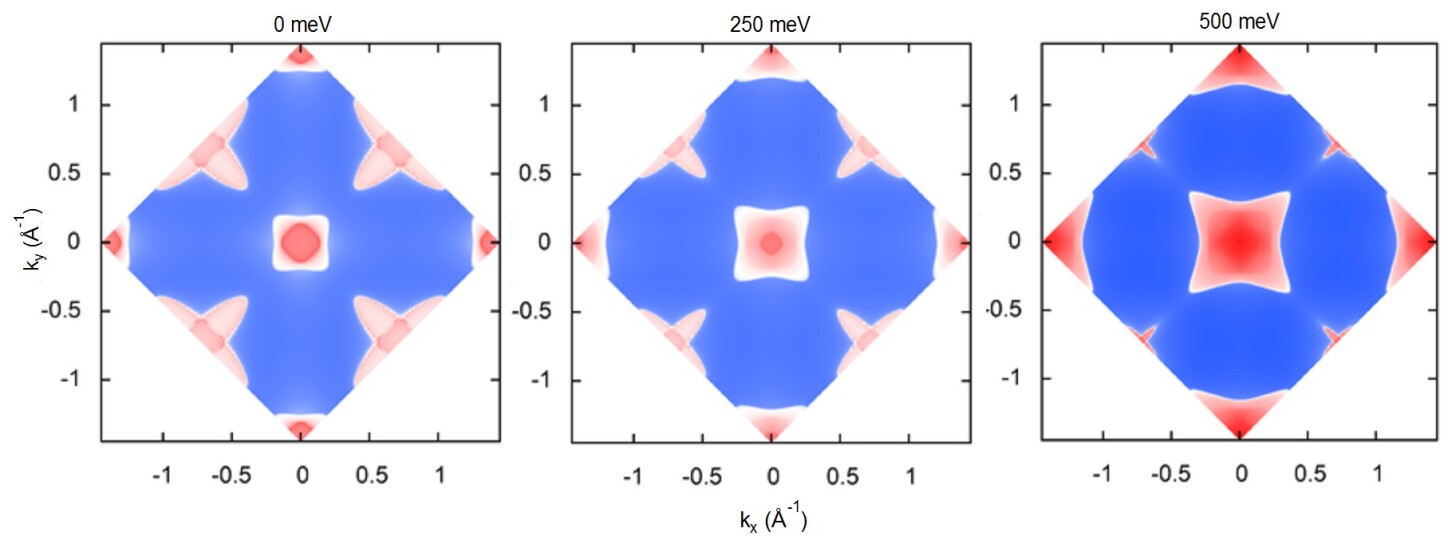
We now discuss the bulk band structure and the Fermi surface using our measured constant energy contours for the (001) surface, see Fig. 2(a). denotes the center, X the corner and M the midpoint between the two corners of the BZ. At the point, we observe a diamond-like outer Fermi pocket and a circular inner pocket. Moving towards higher binding energies, we observe a third band and that the size of the pockets increases, confirming the hole-like nature of the bands around . At the point, we clearly see two concentric elliptical-shaped pockets. However, moving to higher binding energies, the elliptical-pockets evolve into point-like features around 460 meV, which indicates the electron-like nature of the bands around the point. Importantly, our calculations show the presence of a local band gap near this binding energy at the point. Around the binding energy of 600 meV, size of the elliptical pocket increases, suggesting that the possible bulk bandgap lies around this binding energy. We will return below to present additional photon energy-dependent dispersion maps around the and points in order to ascertain the nature of the bands from our experimental measurements. Figure 2(b) shows the calculated Fermi surface contour, which is in substantial agreement with our experimental results.
Trivial electronic structures of HoSb
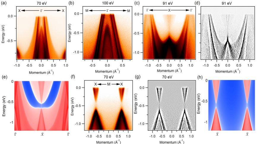
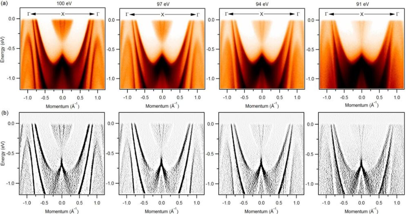
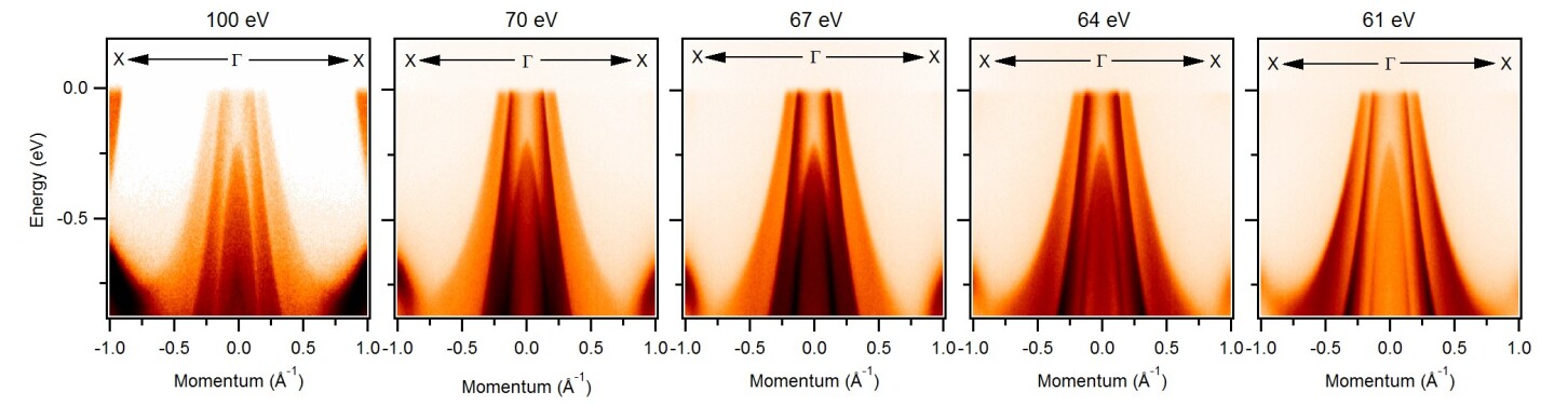
Figure 3 presents energy dispersion maps along the high-symmetry directions in the BZ. Figure 3(a) shows the energy dispersion along the direction measured at a photon energy of 70 eV. Two hole-bands are observed to cross the Fermi level while the top of a third hole-band can be seen at around 200 meV below the Fermi level. Figure 3(b) shows the measured dispersion map around the point along the high-symmetry direction . Similar to Fig. 3(a), three hole-bands are observed with two bands crossing the Fermi level. Importantly, two bands crossing the Fermi level along the direction are sharply dispersive in comparison to the direction, which indicates the highly anisotropic nature of these bands and also explains the distortion of the diamond-shaped pocket as we move towards higher binding energies in Fig. 2. Figures 3(c) and,(d) show the dispersion map and the second derivative plots of the spectra along the direction at a photon energy of 91 eV. One can observe the gapped Dirac-like state at the X points of the BZ. The bulk band gap at the X point is better resolved in the second derivative plot (see also Supplementary Fig. 3(b)). Notably, the preceding experimental results are in substantial accord with our theoretically predicted dispersions in Fig. 3(e).
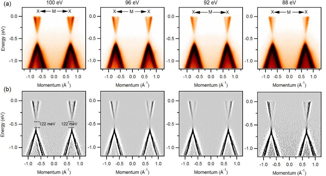
We further confirm this by presenting photon energy dependent dispersion nature of the bands along the X-M-X direction and its second derivative in Figs. 3(f), (g) (see also Supplementary Fig. 5), respectively. The experimentally observed bulk band gap is approximately 120 meV. Figure 3(h) shows that the calculated dispersion along the - line is in excellent accord with the correponding experimental results. The theoretical bulk band gap at the point is about 90 meV. There is a continuous band gap between the valence and conduction bands so that the 2 invariant is well defined. Using the evolution of Wannier charge centers Z2 , we find a trivial topological invariant 2=0. In this way, we conclude that HoSb is a trivial semimetal and not a topological semimetal.
Transport signature of electron-hole compensation
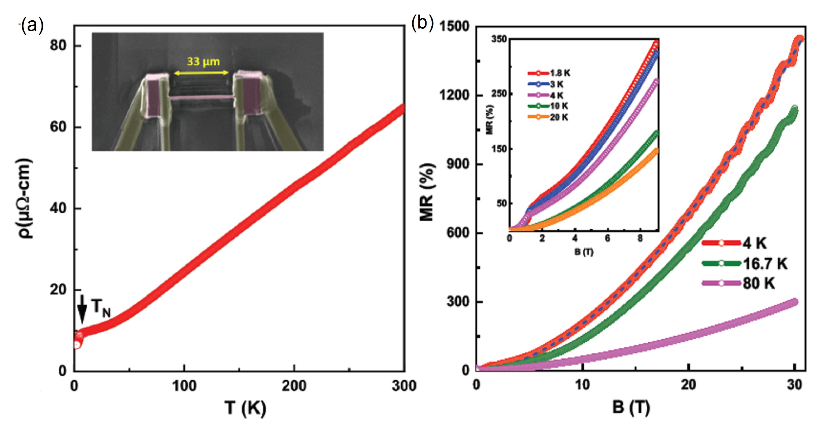
Our ARPES measurements indicate that HoSb is a trivial semimetal. In order to study the transport properties of HoSb, we used a micron-sized sample prepared by plasma focused ion beam (PFIB) microscope. Magneto-transport measurements were performed on a FIB′ed single crystal, where the electrical current (i) was applied along the [100] crystallographic direction and the magnetic field was applied perpendicular to i and [100] (see inset in Figure 4(a)). Temperature dependence of electrical resistivity of the HoSb single crystal is shown in Fig. 4(a). The overall behavior of (T) and the presence of an antiferromagnetic ordering at TN = 5.7 K agrees well with previous studies Xia1 . Application of magnetic field strongly increases electrical resistivity and (T) curve saturates at lower temperatures (the resistivity plateau) Xia1 . The field dependent resistivity saturation at low temperatures has not been observed in the non-magnetic members of the REM family Niu . The origin of such a plateau has been recently attributed to the presence of a nearly perfect electron-hole carrier compensation and the high mobility of the compensated semimetals Guo1 . Figure 4(b) and its inset show the magnetic field dependence of transverse magnetoresistance of HoSb at various temperatures. Magnetoresistance denotes the change of the electrical resistance under applied magnetic field defined as, MR = [()-(0)]/(0), where () and (0) are resistances with and without the magnetic field, respectively. As seen from the inset of Fig. 4 (b), at temperatures below and above , MR increases with the increasing magnetic field. The kinks in the MR() curves mark a metamagnetic transition that is related to the change in the magnetic structure with the increase of field Magnetic . At = 1.8 K, magnetoresistance is large, reaching 350 at 9 T without any sign of saturation, in agreement with previous reports Xia1 . In this connection, we measured MR in pulsed magnetic fields up to 30 T (Fig. 4(b)), and found MR measured at several temperatures below and above the Neel temperature increases with magnetic field. MR reaches a large values of about 1500 at 30 T ( = 4 K) which is comparable to the values observed in topological semimetals LaSb LaSb , NbP NbP , and WTe2 Mazhar . The MR() curve at 4 K can be described by the form MR (see dashed line in Fig. 4b), where = 1.75. The close proximity to quadratic field dependence indicates nearly complete electron-hole compensation in HoSb, as expected from a semiclassical two-band model Guo1 . In addition, for = 4 K and 16 K, obvious Shubnikov-de Haas (SdH) oscillations are observed at high fields. The presence of the quantum oscillations, even at 16 K, points to the high quality of our HoSb single crystals used in the present studies. Analysis of SdH data in fields up to 30 T will be shown elsewhere. It is also the characteristic of low effective mass and large mobility of carriers that could exist in HoSb. The large, non-saturating magnetoresistance, the resistivity saturation in the turn-on temperature behavior at very low temperatures together with metallic conductivity observed in HoSb are all comparable to the characteristic of topological electron-hole-compensated semimetals Guo1 ; ehcom .
Discussion
We have carried out in-depth photoemission and transport measurements on HoSb single crystals along with parallel first-principles modeling of the electronic structure of this member of the REM family. Our ARPES measurements show the presence of Dirac-like cone with a small gap at around 470 meV below the chemical potential, but our analysis shows that HoSb is a trivial and not a topological Dirac semimetal. The observed experimental bulk band gap at X point is around 120 meV which is consistent with the theoretically predicted value. Magnetoresistance is found to be large and non-saturating, even at a magnetic field as large as 30 T. The characteristic behavior of electrical resistivity at low temperatures indicates that HoSb is likely a new electron-hole-compensated semimetal. Notably, the XMR effect has also been reported in other nontrivial members of the REM family suggesting that the presence of non-trivial state might not be directly responsible for the XMR. However, the high carrier mobility associated with the topological states might play a role in generating the XMR. Furthermore, our magnetoresitivity measurements up to 30 T show a similar unsaturated behavior below and above TN indicating similarity of the overall Fermi surface topology in the vicinity of Fermi energy above and below the Neel temperature. Keeping in mind that the rare-earth monopnictide family can host complex magnetic structures including the possibility of a Devil’s Staircase transition DS , HoSb offers a unique platform for exploring the interplay between XMR, magnetism and topology in an antiferromagnetic matrix.
Methods
Crystal growth and characterization
Single crystals of HoSb were grown by the Sn flux technique as described elsewhere Growth . The crystal structure was determined by X-ray diffraction on a Kuma-Diffraction KM4 four-circle diffractometer equipped with a CCD camera using Mo K radiation, while chemical composition was checked by energy dispersive X-ray analysis using an FEI scanning electron microscope equipped with an EDAX Genesis XM4 spectrometer.
Spectroscopic characterization
Synchrotron-based ARPES measurements of the electronic structure were performed at the Advanced light Source (ALS) beamline 4.0.3 with a Scienta R8000 hemispherical electron analyzer. The samples were cleaved in situ in a ultra high vacuum conditions (510-11 Torr) at 18 K. The energy resolution was set to be better than 20 meV. The angular resolution was set to be better than 0.2∘ for the synchrotron measurements.
Transport measurements
For transport measurements, the HoSb sample was prepared by a Plasma Focused Ion Beam (PFIB) method. The electrical resistivity and magnetoresistivity were measured using a Quantum Design Dynacool-9 device in magnetic field up to 9 T. Magnetoresistance measurements at pulsed magnetic fields up to 30 T were performed at NHMFL, and LANL using the same HoSb sample as that used in DC fields. For both measurements, a standard four probe measurement technique was applied.
Theoretical calculations
Electronic structure calculations were performed within the framework of the density-functional theory (DFT) using the projector-augmented-wave (PAW) method PAW as implemented in the VASP suite of codes dft ; vasp . The exchange-correlation functional was treated using SCAN meta-GGA SCAN . An energy cutoff of 400 eV was used for the plane-wave basis set and a -centered 111111 k-mesh was used for BZ integrations. In order to examine the topological properties, we constructed a tight-binding model with atom-centered Wannier functions using the VASP2WANNIER90 interface Wannier . The surface energy spectrum was obtained by using the iterative Green’s function method via the WannierTools package DFT ; Green2 ; Green1 .
Data availability
All data will be made available by the corresponding author upon request.
References
- (1) Hasan, M. Z. & Kane, C. L. Colloquium: topological insulators. Rev. Mod. Phys. , 3045-3067 (2010).
- (2) Xia, Y. et al. Observation of a large-gap topological-insulator class with a single Dirac cone on the surface. Nat. Phys. , 398 (2009).
- (3) Hasan, M. Z., Xu, S.-Y. & Neupane, M. Topological Insulators: Fundamentals and Perspectives, (John Wiley and Sons, New York, 2015).
- (4) Bansil, A., Lin, H. & Das, T. Colloquium: Topological band theory. Rev. Mod. Phys. , 021004 (2016).
- (5) Wang, Z., Weng, H., Wu, Q., Dai, X. Fang, Z. Three-dimensional Dirac semimetal and quantum transport in Cd3As2. Phys. Rev. B , 125427 (2013).
- (6) Neupane, M. et al. Observation of a three-dimensional topological Dirac semimetal phase in high-mobility Cd3As2. Nat. Commun. , 3786 (2014).
- (7) Xu, S.-Y. et al. Discovery of a Weyl Fermion Semimetal and Topological Fermi Arcs. Science 349, 613 (2015).
- (8) Lv, B. Q. et al. Experimental Discovery of Weyl Semimetal TaAs. Phys. Rev. X 5, 031013 (2015).
- (9) Neupane, M. et al. Observation of topological nodal fermion semimetal phase in ZrSiS. Phys. Rev. B 93, 201104(R) (2016).
- (10) Yoshomi, R. et al. Dirac electron states formed at the heterointerface between a topological insulator and a conventional semiconductor. Nat. Mater. 13, 253-257 (2014).
- (11) Fu, L. & Kane, C. L. Topological Insulators with Inversion Symmetry. Phys. Rev. B 76, 045302 (2007).
- (12) Zhao, Y. X. & Wang, Z. D. Novel Topological Metals and Semimetals. Phys. Rev. Lett. 116, 016401 (2016).
- (13) Zeng, M. et al. Topological semimetals and topological insulators in rare earth monopnictides. arXiv:1504.03492 (2015).
- (14) He, J. et al. Distinct Electronic Structure for the Extreme Magnetoresistance in YSb. Phys. Rev. Lett. 117, 267201 (2016).
- (15) Yang, H.-Y et al. Extreme magnetoresistance in the topologically trivial lanthanum monopnictide LaAs. Phys. Rev. B 96, 235128 (2017).
- (16) Pavlosiuk, O., Swatek, P., Kaczorowski D. & Wiśniewski, P. Magnetoresistance in LuBi and YBi semimetals due to nearly perfect carrier compensation. Phys. Rev. B 97, 235132 (2018).
- (17) Guo, C. et al. Possible Weyl fermions in the magnetic Kondo system CeSb. npj Quantum Mater. 2, 39 (2017).
- (18) Liang, D. D. et al. Extreme magnetoresistance and Shubnikov-de Haas oscillations in ferromagnetic DySb. APL Materials 6, 086105 (2018).
- (19) Yu, Q.-H. et al. Magnetoresistance and Shubnikov-de Haas oscillation in YSb. EPL 119, 17002 (2017).
- (20) Yang, H.-Y. et al. Interplay of Magnetism and Transport in HoBi. Phys. Rev. B 98, 045136 (2018).
- (21) Pavlosiuk, O., Swatek, P. & Wiśniewski, P. Giant magnetoresistance, three-dimensional Fermi surface and origin of resistivity plateau in YSb semimetal. Sci. Rep. 6, 38691 (2016).
- (22) Pavlosiuk, O., Kleinert, M., Swatek, P., Kaczorowski, D. & Wiśniewski, P. Fermi surface topology and magnetotransport in semimetallic LuSb. Sci. Rep. 7, 12822 (2017).
- (23) Ali, M. N. et al. Large, non-saturating magnetoresistance in WTe2. Nature 514, 205 (2014).
- (24) Liang, T., Gibson, Q., Ali, M. N., Liu, M., Cava R. J. & Ong, N. P. Ultrahigh mobility and giant magnetoresistance in the Dirac semimetal Cd3As2. Nat. Mater. 14, 280 (2015).
- (25) Mun, E., Ko, H., Miller, G. J., Samolyuk, G. D., Bud’ko, S. L. & Canfield, P. C. Magnetic field effects on transport properties of PtSn4. Phys. Rev. B 85, 035135 (2012).
- (26) Huang, X. et al. Observation of the Chiral-Anomaly-Induced Negative Magnetoresistance in 3D Weyl Semimetal TaAs. Phys. Rev. X 5, 031023 (2015).
- (27) Wu, Y. et al. Asymmetric mass acquisition in LaBi: Topological semimetal candidate. Phys. Rev. B 94, 081108(R) (2016).
- (28) Niu, X. H. et al. Presence of exotic electronic surface states in LaBi and LaSb. Phys. Rev. B 94, 165163 (2016).
- (29) Nayak, J. et al. Multiple Dirac cones at the surface of the topological metal LaBi. Nat. Commun. 8, 13942 (2017).
- (30) Lou, R. et al. Evidence of topological insulator state in the semimetal LaBi. Phys. Rev. B 95, 115140 (2017).
- (31) Nummy, T. J. et al. Measurement of the atomic orbital composition of the near-fermi-level electronic states in the lanthanum monopnictides LaBi, LaSb, and LaAs. npj Quantum Mater. 3, 24 (2018).
- (32) Feng, B. et al. Experimental observation of node-line-like surface states in LaBi. Phys. Rev. B 97, 155153 (2018).
- (33) Zeng, L.-K. et al. Compensated Semimetal LaSb with Unsaturated Magnetoresistance. Phys. Rev. Lett. 117, 127204 (2016).
- (34) Oinuma, H. et al. Three-dimensional band structure of LaSb and CeSb: Absence of band inversion. Phys. Rev. B 96, 041120(R) (2017).
- (35) Alidoust, N. et al. A new form of (unexpected) Dirac fermions in the strongly-correlated cerium monopnictides. arXiv:1604.08571 (2016).
- (36) Kuroda, K. et al. Experimental Determination of the Topological Phase Diagram in Cerium Monopnictides. Phys. Rev. Lett. 120, 086402 (2018).
- (37) Ye, L., Suzuki, T., Wicker, C. R. & Checkelsky, J. G. Extreme magnetoresistance in magnetic rare-earth monopnictides. Phys. Rev. B 97, 081108 (2018).
- (38) Neupane, M. et al. Observation of Dirac-like semi-metallic phase in NdSb. J. Phys. Cond. Mater. 28, 23LT02 (2016).
- (39) Busch, G. & Vogt, O. Magnetic Anisotropies in Antiferromagnetic Rare Earth Antimonide Single Crystals. J. Appl. Phys. 39, 1334 (1968).
- (40) Child, H. R., Wilkinson, M. K., Cable, J. W., Koehler, W. C. & Wollan, E. O. Neutron Diffraction Investigation of the Magnetic Properties of Compounds of Rare-Earth Metals with Group V Anions. Phys. Rev. 131, 922 (1963).
- (41) Wang, Y.-Y., Sun, L.-L, Xu, S., Su Y. & Xia, T.-L. Unusual magnetotransport in holmium monoantimonide. Phys. Rev. B 98, 045137 (2018).
- (42) Kulshrestha, S., Rana, P., Singh, S. K. & Gupta, D. C. Electronic and Thermal Properties of HoSb Under Pressure: A LSDA+U Study. AIP Conference Proceedings 1349, 797 (2011).
- (43) Canfield, P. C. & Fisk, Z. Growth of single crystals from metallic fluxes. Phil. Mag. B 65, 1117 (1992).
- (44) Yu, R., Qi, X. L., Bernevig, A., Fang, Z. & Dai, X. Equivalent expression of 2 topological invariant for band insulators using the non-Abelian Berry connection. Phys. Rev. B 84, 075119 (2011).
- (45) Guo, P.-J., Yang, H.-C., Zhang, B.-J., Liu, K. & Lu, Z.-Y. Charge compensation in extremely large magnetoresistance materials LaSb and LaBi revealed by first-principles calculations. Phys. Rev. B 93, 235142 (2016).
- (46) Brun, T. O., Korty, F. W. & Kouvel, J. S. Quadropolar interactions and the magnetic states of HoSb. J. Magn. Magn. Mater. 15, 298 (1980).
- (47) Tafti, F. F., Gibson, Q. D., Kushwaha, S. K. Haldolaarachchige, N. & Cava, R. J. Resistivity plateau and extreme magnetoresistance in LaSb. Nat. Phys. 12, 272 (2016).
- (48) Shekhar, C. et al. Extremely large magnetoresistance and ultrahigh mobility in the topological Weyl semimetal candidate NbP. Nat. Phys. 11, 645 (2015).
- (49) Leahy, I. A. et al. Nonsaturating large magnetoresistance in semimetals. PNAS 10, 1073 (2018).
- (50) Bychkov, Y. A. & Rashba, E. I. Properties of a 2D electron gas with lifted spectral degeneracy. JETP Lett. 39, 78 (1984).
- (51) Kuroda, K. et al., Devil’s staircase transition of the electronic structures in CeSb, Nat. Commun. 11,2888 (2020).
- (52) Blchl, P. E. Projector augmented-wave method. Phys. Rev. B 50, 17953 (1994).
- (53) Kresse, G. & Hafner, j. Ab initio molecular dynamics for liquid metals. Phys. Rev. B 47, 558 (1993).
- (54) Kresse, G. & Furthmller, Efficiency of ab-initio total energy calculations for metals and semiconductors using a plane-wave basis set. J. Computational Materials Science 6, 15 (1996).
- (55) Sun, J., Ruzsinszky, A. & Perdew, J. P. Strongly constrained and appropriately normed semilocal density functional. Phys. Rev. Lett. 115, 036402 (2015).
- (56) Mostofi, A. A. et al. An updated version of wannier90: A tool for obtaining maximally-localised Wannier functions. Comput. Phys. Commun. 185, 2309 (2014).
- (57) Wu, Q., Zhang, S., Song, H.-F., Troyer, M. & Soluyanov A. A. Comput. Phys. Commun. 224, 405 (2018).
- (58) Lopez Sancho, M. P., Lopez Sancho J. M. & Rubio, J. Quick iterative scheme for the calculation of transfer matrices: application to MO( 100). J. Phys. F: Met. Phys. 14, 1205 (1984).
- (59) Lopez Sancho, M. P., Lopez Sancho J. M. & Rubio, J. Highly convergent schemes for the calculation of bulk and surface Green functions. J. Phys. F: Met. Phys. 15, 851 (1985).
Acknowledgment
M.N. is supported by the Air Force Office of Scientific Research under Award No. FA9550-17-1-0415 and the Center for Thermal Energy Transport under Irradiation, an Energy Frontier Research Center funded by the U.S. DOE, Office of Basic Energy Sciences.
D.K., O.P. and P.W. are supported by the National Science Centre (Poland) under research grant 2015/18/A/ST3/00057. O.P. is supported by the Foundation for Polish Science (FNP), program START 66.2020.
The work at Northeastern University was supported by the US Department of Energy (DOE), Office of Science, Basic Energy Sciences grant number DE-FG02-07ER46352, and benefited from Northeastern University’s Advanced Scientific Computation Center (ASCC) and the NERSC supercomputing center through DOE grant number DE-AC02-05CH11231. K.G. acknowledges support from the DOE’s Early Career Research Program. N.P acknowledges support from INL’s LDRD program (18P37-008FP). Work performed at the NHMFL is supported by NSF cooperative agreement No. DMR-1644779, the State of Florida and DOE. This research used resources of the Advanced Light Source, a U.S. Department of Energy Office of Science User Facility, under Contract No. DE-AC02-05CH11231.
We thank Sung-Kwan Mo and Jonathan Denlinger for beamline assistance at the LBNL.
Author contributions
M.N. conceived the study; D.K., P.W. and O.P. synthesized the single crystals and performed the transport characterizations; K.G., N.P., F.W. and D. M. prepared the Plasma Focused Ion Beam sample and performed magnetotransport measurements; M.M.H. and M.N. performed the measurements and analysis with the help of G.D., K.D., F.K., C.S., S.R., and W. N.; M.M.H. and M.N. performed the figure planning; B.W., B.S., A.B.S., A.A, and A.B. performed and analyzed the first-principles calculations; A.B. was responsible for the theoretical research direction; M.M.H. and M.N. wrote the manuscript with input from all authors; M.N. was responsible for the overall research direction, planning and integration among different research units.
Competing interests
The Authors declare no Competing Financial or Non-Financial interests.
Correspondence and requests for materials should be addressed to M.N. (Email: Madhab.Neupane@ucf.edu).
Supplementary Information
Observation of gapped state in rare-earth monopnictide HoSb
This file includes
Supplementary figure 1: Fermi surface and constant energy contour plots.
Supplementary figure 2: Calculated Fermi surface and constant energy contour plots of HoSb.
Supplementary figure 3: Dispersion maps along the -M- high symmetry direction.
Supplementary figure 4: Observation of bulk bands around the zone center.
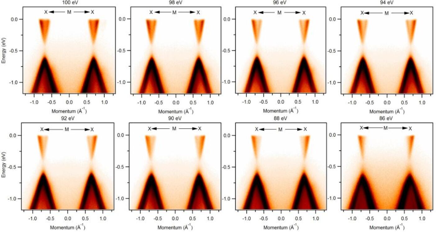
Supplementary figure 5: Experimental photon energy dependent dispersion maps along the X-M-X direction.
Supplementary figure 6: Confirmation of gapped state.
Supplementary note 1: Fermi surface and constant energy contour plots of HoSb
Supplementary note 2: Observation of the gapped state
Supplementary Note 1
Fermi surface and constant energy contour plots of HoSb
We measured a second batch of samples to access the robustness of our Fermi surface and electronic structures results. Supplementary Figure (SF) 1 shows the observed Fermi surface (SF. 1(a)-(b)) and the related constant energy contour plots (SF. 1(c)-(f)) for the new measurements. Like the Fig. 1 in the main text, Fermi surface consists of an outer diamond and an inner circular pocket at the point (zone center) and two concentric elliptical pockets at the X point of the Brillouin zone (BZ) (SF. 1(a)-(b)). Importantly, at a higher binding energy (470 meV), we observe that the elliptical-pocket evolves into a point-like feature. Supplementary Figure 2 shows the corresponding calculated Fermi surface and the related constant energy contour plots. An excellent agreement is seen between the experimental data and theoretical predictions.
Supplementary Note 2
Observation of the gapped state
In order to determine the origin of the bands near the zone center and the corner of the BZ, we performed photon energy dependent dispersion maps around these high-symmetry points. Supplementary Figures 3(a) and,(b) show the measured photon energy dependent dispersion maps and their second derivative plots along the -X- direction, respectively. Around the point, two hole-like bands cross the Fermi level while at the X point, we observe a nearly linearly dispersive feature. To confirm the origin of the bands near the point, we present more photon energy dependent dispersion maps in Supplementary Fig. 4 over a wide energy window. Here, one can clearly observe the photon energy dependent dispersive nature of the bands, so that the hole-like bands at around the zone center are bulk originated. Furthermore, from Supplementary Figure 3(b), we see a clear gap at the X point. In order to further confirm the gapped state at the X point, we present photon energy dependent dispersion maps along the X-M-X direction in the supplementary Fig. 5. The gapped state is seen consistently at all photon energies. In order to observe the gap size more vividly, we present measured dispersion maps and their second derivative plots in Supplementary Fig. 6. From panel 6(b), we approximate the band gap size around 120 meV. Moreover, the bulk state is once again clearly observed to be gapped which is consistent with the main text results.