Selecting “Convenient Observers” to Probe the Atomic Structure of Epitaxial Graphene Grown on Ir(111) via Photoelectron Diffraction
Abstract
Epitaxial graphene grown on metallic substrates presents, in several cases, a long-range periodic structure due to a lattice mismatch between the graphene and the substrate. For instance, graphene grown on Ir(111), displays a corrugated supercell with distinct adsorption sites due to a variation of its local electronic structure. This type of surface reconstruction represents a challenging problem for a detailed atomic surface structure determination for experimental and theoretical techniques. In this work, we revisited the surface structure determination of graphene on Ir(111) by using the unique advantage of surface and chemical selectivity of synchrotron-based photoelectron diffraction. We take advantage of the Ir 4f photoemission surface state and use its diffraction signal as a probe to investigate the atomic arrangement of the graphene topping layer. We determine the average height and the overall corrugation of the graphene layer, which are respectively equal to 3.40 0.11 Å and 0.45 0.03 Å. Furthermore, we explore the graphene topography in the vicinity of its high-symmetry adsorption sites and show that the experimental data can be described by three reduced systems simplifying the Moiré supercell multiple scattering analysis.
I Introduction
Since the isolation of a single graphene layer Novoselov et al. (2004), a considerable effort has been performed to develop and modify fabrication processes to improve its quality Lee et al. (2019). In this context, the synthesis of graphene on single-crystal metallic surfaces via chemical vapor deposition is a well-established route to obtain high-quality large-area graphene layers Wintterlin and Bocquet (2009); Batzill (2012); Lizzit et al. (2012). Particularly, Ir(111) is a notable substrate to grow graphene. First, under certain controllable conditions, it is possible to systematically obtain a full single layer without rotational domains Hattab et al. (2011). Second, the graphene-substrate interaction is relatively weak such that the graphene -band is almost intactPletikosić et al. (2009); Kralj et al. (2011). Actually, the electronic structure, which presents mini gaps and replica bands, can be tuned and chemically decoupled from the substrate by intercalationLarciprete et al. (2012); Ulstrup et al. (2014); Pervan and Lazić (2017); Balog et al. (2019).
From the structural point of view, graphene grown on iridium (Gr/Ir) presents a lattice mismatch between the carbon layer and the underlying substrate, which forms a moiré superstructure Dedkov and Voloshina (2015). The large periodicity of the moiré superlattice is reflected on a variation of the carbon substrate distance through the supercell such that the graphene layer displays a corrugated feature leading to a modulation of the electronic density Voloshina et al. (2013). Therefore, the adsorption behavior along the moiré cell can vary significantly. In this sense, such moiré structures can be used as a template to form highly ordered dispersed nanostructures. For instance, Gr/Ir has been used to create periodic ordered metallic nanoclusters N’Diaye et al. (2006) and atomic periodic superlattices Baltic et al. (2016); Petrović et al. (2017); Pivetta et al. (2018).
The interest in Moiré structures go beyond graphene on metals. For example, transition metal dichalcogenides such as MoS2 and WSe2 both grown on Au(111) exhibit a corrugated Moiré structure Sørensen et al. (2014); Grønborg et al. (2015); Dendzik et al. (2015), also hexagonal boron nitride (h-BN) grown on several metallic substrates shows similar features Auwärter (2019). Moreover, the weak interaction between layers in two-dimensional materials opens the possibility of stacking atomic layers with different lattice parameters forming a Moiré superlattice. One can also form a long-range ordered structure twisting two layers of the same material Cheng et al. (2019). In those structures, the electrons are under the influence of a long-range potential, which can lead to emergent phenomena such as superconductivity and formation of flat bands Cao et al. (2018); Zhao et al. (2020).
The position of the carbon atoms on the corrugated graphene layer is directly connected to its local electronic structure. Therefore, determining the surface topography is crucial to understand the behavior of the different adsorption sites. The modulated surface can be directly observed by imaging techniques such as Atomic Force Microscopy (AFM) Hämäläinen et al. (2013) and Scanning Tunnelling Microscopy (STM) N'Diaye et al. (2008); de Campos Ferreira et al. (2018). Furthermore, the modulation can also be identified via Low Energy Electron Diffraction (LEED), where satellites surround the main reflection spots of the substrate Hattab et al. (2011).
In order to determine the distance between the carbon layer and the substrate, it is necessary to use scattering techniques Busse et al. (2011); Jean et al. (2015). Although LEED is mostly used to examine the quality of graphene grown on metallic substrates Hattab et al. (2011); Rogge et al. (2015), the quantitative LEED analysis is challenging since one has to deal with dynamical scattering calculations on a considerably large unit cell. For instance, in the case of Gr/Ir and Gr/Ru, the typical unit cells consider hundreds of scattering centersMoritz et al. (2010); Hämäläinen et al. (2013). In fact, a proper structural characterization of those long-range superstructures demands novel description methodologies Hermann (2012); Zeller and Günther (2014); Moritz (2015); Zeller et al. (2017); Kuznetsov et al. (2018); Ster et al. (2019); de Lima et al. (2020).
In this work, we investigate the Gr/Ir atomic structure via synchrotron-based X-ray Photoelectron Diffraction (XPD). We use the substrate diffraction signal to probe the graphene structureMuntwiler et al. (2001). Notably, we have selected the photoelectrons from the topmost substrate layer due to the presence of the iridium surface state. This approach makes the XPD signal much more sensitive to the C layer, avoiding the strong forward scattering on Ir layers observed for the Ir bulk signal. Therefore, the unique chemical selectivity of the technique combined with the chance of selecting the photon energy allows us to increase the probability of having scattering events at the carbon layer. Instead of performing the XPD multiple scattering analysis on the entire supercell, we reduce the Gr/Ir Moiré superstructure into three reduced clusters. Based on the location of the high-symmetry sites, we select one electron emitter, a convenient observer, on each cluster to probe the graphene topography around the selected emitter. Although this approach does not consider the problem extensively, it dramatically reduces the computation effort for the complex surface structure determination allowing us to describe the corrugated Gr/Ir atomic structure with an acceptable agreement between theory and experiment.
II Methods
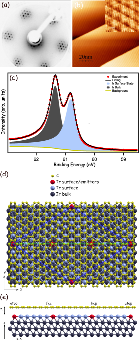
The Ir(111) crystal was cleaned by sputtering using 1.0 KeV Ar ions followed by flash annealing up to 1570 K. A full graphene layer was obtained via thermal decomposition of hydrocarbons: the sample was kept at 1570 K in a mbar propylene background pressure. From the LEED pattern exhibited in the inset figure 1a, it is possible to conclude that the graphene does not present rotational domains Hattab et al. (2011); Rogge et al. (2015). Moreover, the STM images in figure 1b reinforce the high quality of the graphene layer since a low defect density is observed. For the structural determination, we performed angle scan synchrotron-based XPD measurements combined with multiple scattering analysis using the Multiple Scattering Calculation of Diffraction (MSCD) package Rehr and Albers (1990); Chen et al. (1998). Based on an atomic cluster, we calculate the theoretical diffraction pattern and compare it with the experimental data through a reliability factor () defined in such a way that indicates a perfect agreement between theory and experiment de Siervo et al. (2002); Soares et al. (2002). Thus a set of parameters, in a trial and error approach, is varied to minimize . See supplemental material for a detailed description of the XPD experimentCezar et al. (2013), structural determination, and error analysis Booth et al. (1997); Pendry (1980); Bondino et al. (2002).
III Discussion and Results
For the clean Ir(111) surface, the Ir 4f7/2 XPS spectrum exhibits two components: the lower binding energy peak is a surface state (SS) associated with the topmost iridium atomic layer, and the other component is related to the underlying atoms van der Veen et al. (1980); Bianchi et al. (2009); de Campos Ferreira et al. (2018). Figure 1c shows a high-resolution XPS of Gr/Ir where it is possible to observe the iridium SS, which is not affected by the presence of the carbon layer Lacovig et al. (2009); Larciprete et al. (2012); de Campos Ferreira et al. (2018). Therefore, for the structural analysis, we use the diffraction signal originated from the SS peak to narrow down the number of emitters and concentrate on the first iridium atomic layer, represented by red and blue in figures 1d-e. However, even in this scenario, the number of emitters is considerably large for a typical XPD multiple scattering calculation. For this reason, in the simulations, we only consider three emitters in the entire unit cell, which are shown in red in figures 1d-e. The selection of those specific emitters is related to their proximity to the high-symmetry graphene adsorption sites: atop, fcc and hcp.
The experimental diffraction pattern obtained from the Ir 4f7/2 SS is exhibited in figure 2a. Notably, the kinetic energy of the photoelectrons is eV, which leads to an inelastic mean free path lower than Å on iridium Tanuma et al. (1991); Powell and Jablonski (2010). Therefore, the possibility of selecting the Ir SS photoelectrons combined with their low kinetic energy increases the surface sensitivity. The former reduces the forward focusing contributions of the inner Ir layers present in the Ir 4f bulk signal. The latter decreases the probability of electrons that eventually travel into deep layers of the substrate through backscattering reaching the detector. Additionally, the distance between the selected emitters in the supercell is Å such that their contributions to the diffraction pattern can be isolated or, put differently, their contribution to the total intensity can be summed incoherently. On that premise, we split the supercell into three clusters with a semi ellipsoidal shape Chen et al. (1998) centered on each emitter. Figures 2b, c, and d show, respectively, the top view of the clusters associated to the atop, fcc and hcp sites; each of them has more than 370 atoms and a surface radius equal to 11 Å.
The graphene-iridium distance () variation through the unit cell leads to a large number of structural parameters to be determined. Since it is possible to observe a smooth graphene topography via scanning probe techniques such as AFM and STM Hämäläinen et al. (2013); Ulstrup et al. (2014); de Campos Ferreira et al. (2018), we assume that the graphene topography can be described by continuous functions, particularly Gaussian functions de Lima et al. (2013); Ulstrup et al. (2018). Similarly, in some structural studies, is expressed by a truncated Fourier series Busse et al. (2011); Hämäläinen et al. (2013); Jean et al. (2015). In contrast, for h-BN grown on Rh(111), the height transition along the supercell is so abrupt that the h-BN topography can be modeled by distinct flat areas de Lima et al. (2020). Here, the graphene-substrate separation at an in-plane location (see figure 1d) on each cluster is described by:
| (1) |
where and are, respectively, the parameters related to the Gaussian amplitude and width, the pair (,) is the location of the emitter and is a distance offset, see figure 1e. The index in equation 1 is related to the three considered emitters, which are termed based on their proximity to the graphene site. For example, the atop emitter is located under the atop graphene adsorption site. The same procedure is used to label the other emitters.
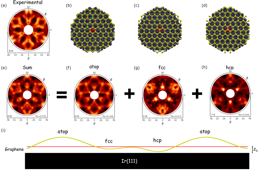
The diffraction pattern which provides the best agreement between theory and experiment is shown in figure 2e from which we conclude that the proposed model provides a very good description of the experimental data (). The diffraction pattern of each cluster is exhibited in figures 2f-h; an isolated emitter provides an inadequate description of the experimental data, as can be seen by the values. The fitting parameters for the best structure are summarized in table 1. For the fcc and hcp sites, the Gaussian prefactor is negative, indicating that in the vicinity of those emitters, the carbon atoms are closer to the substrate. Inversely, in the atop site, the graphene layer is located at a higher distance from the substrate. We also investigated the presence of buckling in the graphene layer, but, differently from graphene on SiC de Lima et al. (2013, 2014a, 2014b) and black phosphorus de Lima et al. (2016), we could not identify any significant vertical displacement between the surface sublattices. A profile along the green line of figure 1d is displayed in figure 2i. The graphene layer is closer to the substrate in the hcp site in agreement with previous structural analysis Busse et al. (2011); Hämäläinen et al. (2013).
| fcc | hcp | top | |
|---|---|---|---|
| Ai (Å) | -0.14 0.02 | -0.19 0.02 | 0.26 0.02 |
| Bi (Å2) | 65 12 | 38 10 | 90 11 |
| zo (Å) | 3.39 0.03 | ||
The overall corrugation () is evaluated as the difference between the highest and lowest graphene distance from the substrate. Furthermore, the coordinates of the carbon atoms on each cluster are used to estimate the graphene mean height (). The obtained values are summarized in table 2 where the same parameters obtained by other techniques are also listed. The overall graphene corrugation agrees, within the error bars, with LEEDHämäläinen et al. (2013), AFMHämäläinen et al. (2013), Surface X-ray Diffraction (SXRD) Jean et al. (2015) and van der Waals-density functional theory (vdW-DFT)Busse et al. (2011) previous studies, but it is lower compared to x-ray standing wave (XSW)Busse et al. (2011). Moreover, the mean height obtained in this work concurs with all previous structural descriptions listed in 2. The concordance of our results with all those techniques reinforces the effectiveness of our simplified description of the problem. For example, a typical periodic model used in this system considers a (10 10) graphene layer on a (9 9) Ir(111) cell. In such a model, we would have to consider 81 nonequivalent emitters for the XPD multiple scattering calculation. However, our result indicates that the chosen emitters already provides an adequate experimental characterization.
| (Å) | (Å) | |
|---|---|---|
| XPD (this work) | 3.40 0.11 | 0.45 0.03 |
| LEEDHämäläinen et al. (2013) | 3.39 0.03 | 0.430.09 |
| AFM Hämäläinen et al. (2013) | - | 0.470.05 |
| SXRDJean et al. (2015) | 3.39 0.28 | 0.3790.044 |
| EXRR Jean et al. (2015) | 3.38 0.04 | - |
| XSW Busse et al. (2011) | 3.38 0.04 | 0.6 0.1 |
| vdW-DFT Busse et al. (2011) | 3.41 | 0.35 |
IV Conclusions
In summary, we have determined the atomic structure of Gr/Ir via XPD. The possibility of discriminating the surface and the bulk iridium photoemission signals allows us to probe the graphene topography using the closest substrate emitters to the carbon atoms. The graphene layer is described by three Gaussian profiles centered on the high-symmetry sites. In the atop region, the carbon atoms are located at the highest distance from the substrate. On the other hand, in the vicinity of the hcp site, the graphene-substrate separation is the shortest. Furthermore, we obtained the mean graphene height and its overall corrugation, which are in agreement with already reported studies indicating that a proper selection of representative emitters can provide a realistic structural characterization of this system via XPD. This approach might be used to study other long-range periodic systems.
Acknowledgements.
This work has been supported by FAPESP (grant nos. 2016/21402-8, 2017/18574-4, 2007/54829-5, and 2007/08244-5), and CNPq (grant no. 401826/2013-9). We thank LNLS for the beamtime, and PGM beamline staff for the technical support. The authors are grateful to the Multiuser Central Facilities CEMs-UFABC for the computational support. DCM acknowledges UFABC for the studentship.References
- Novoselov et al. (2004) K. S. Novoselov, A. K. Geim, S. V. Morozov, D. Jiang, Y. Zhang, S. V. Dubonos, I. V. Grigorieva, and A. A. Firsov, Science 306, 666 (2004).
- Lee et al. (2019) X. J. Lee, B. Y. Z. Hiew, K. C. Lai, L. Y. Lee, S. Gan, S. Thangalazhy-Gopakumar, and S. Rigby, Journal of the Taiwan Institute of Chemical Engineers 98, 163 (2019).
- Wintterlin and Bocquet (2009) J. Wintterlin and M.-L. Bocquet, Surface Science 603, 1841 (2009).
- Batzill (2012) M. Batzill, Surface Science Reports 67, 83 (2012).
- Lizzit et al. (2012) S. Lizzit, R. Larciprete, P. Lacovig, M. Dalmiglio, F. Orlando, A. Baraldi, L. Gammelgaard, L. Barreto, M. Bianchi, E. Perkins, and P. Hofmann, Nano Letters, Nano Lett. 12, 4503 (2012).
- Hattab et al. (2011) H. Hattab, A. T. N’Diaye, D. Wall, G. Jnawali, J. Coraux, C. Busse, R. van Gastel, B. Poelsema, T. Michely, F.-J. M. zu Heringdorf, and M. H. von Hoegen, Applied Physics Letters 98, 141903 (2011).
- Pletikosić et al. (2009) I. Pletikosić, M. Kralj, P. Pervan, R. Brako, J. Coraux, A. T. N’Diaye, C. Busse, and T. Michely, Phys. Rev. Lett. 102, 056808 (2009).
- Kralj et al. (2011) M. Kralj, I. Pletikosić, M. Petrović, P. Pervan, M. Milun, A. T. N’Diaye, C. Busse, T. Michely, J. Fujii, and I. Vobornik, Phys. Rev. B 84, 075427 (2011).
- Larciprete et al. (2012) R. Larciprete, S. Ulstrup, P. Lacovig, M. Dalmiglio, M. Bianchi, F. Mazzola, L. Horneær, F. Orlando, A. Baraldi, P. Hofmann, and S. Lizzit, ACS Nano 6, 9551 (2012).
- Ulstrup et al. (2014) S. Ulstrup, M. Andersen, M. Bianchi, L. Barreto, B. Hammer, L. Hornekær, and P. Hofmann, 2D Materials 1, 025002 (2014).
- Pervan and Lazić (2017) P. Pervan and P. Lazić, Phys. Rev. Materials 1, 044202 (2017).
- Balog et al. (2019) R. Balog, A. Cassidy, J. Jørgensen, L. Kyhl, M. Andersen, A. G. Čabo, F. Ravani, L. Bignardi, P. Lacovig, S. Lizzit, and L. Hornekær, Journal of Physics: Condensed Matter 31, 085001 (2019).
- Dedkov and Voloshina (2015) Y. Dedkov and E. Voloshina, Journal of Physics: Condensed Matter 27, 303002 (2015).
- Voloshina et al. (2013) E. N. Voloshina, E. Fertitta, A. Garhofer, F. Mittendorfer, M. Fonin, A. Thissen, and Y. S. Dedkov, Scientific Reports 3, 1072 (2013).
- N’Diaye et al. (2006) A. T. N’Diaye, S. Bleikamp, P. J. Feibelman, and T. Michely, Phys. Rev. Lett. 97, 215501 (2006).
- Baltic et al. (2016) R. Baltic, M. Pivetta, F. Donati, C. Wäckerlin, A. Singha, J. Dreiser, S. Rusponi, and H. Brune, Nano Letters 16, 7610 (2016).
- Petrović et al. (2017) M. Petrović, P. Lazić, S. Runte, T. Michely, C. Busse, and M. Kralj, Phys. Rev. B 96, 085428 (2017).
- Pivetta et al. (2018) M. Pivetta, S. Rusponi, and H. Brune, Phys. Rev. B 98, 115417 (2018).
- Sørensen et al. (2014) S. G. Sørensen, H. G. Füchtbauer, A. K. Tuxen, A. S. Walton, and J. V. Lauritsen, ACS Nano 8, 6788 (2014).
- Grønborg et al. (2015) S. S. Grønborg, S. Ulstrup, M. Bianchi, M. Dendzik, C. E. Sanders, J. V. Lauritsen, P. Hofmann, and J. A. Miwa, Langmuir 31, 9700 (2015).
- Dendzik et al. (2015) M. Dendzik, M. Michiardi, C. Sanders, M. Bianchi, J. A. Miwa, S. S. Grønborg, J. V. Lauritsen, A. Bruix, B. Hammer, and P. Hofmann, Phys. Rev. B 92, 245442 (2015).
- Auwärter (2019) W. Auwärter, Surface Science Reports 74, 1 (2019).
- Cheng et al. (2019) Y. Cheng, C. Huang, H. Hong, Z. Zhao, and K. Liu, Chinese Physics B 28, 107304 (2019).
- Cao et al. (2018) Y. Cao, V. Fatemi, A. Demir, S. Fang, S. L. Tomarken, J. Y. Luo, J. D. Sanchez-Yamagishi, K. Watanabe, T. Taniguchi, E. Kaxiras, R. C. Ashoori, and P. Jarillo-Herrero, Nature 556, 80 (2018).
- Zhao et al. (2020) X.-J. Zhao, Y. Yang, D.-B. Zhang, and S.-H. Wei, Phys. Rev. Lett. 124, 086401 (2020).
- Hämäläinen et al. (2013) S. K. Hämäläinen, M. P. Boneschanscher, P. H. Jacobse, I. Swart, K. Pussi, W. Moritz, J. Lahtinen, P. Liljeroth, and J. Sainio, Phys. Rev. B 88, 201406 (2013).
- N'Diaye et al. (2008) A. T. N'Diaye, J. Coraux, T. N. Plasa, C. Busse, and T. Michely, New Journal of Physics 10, 043033 (2008).
- de Campos Ferreira et al. (2018) R. C. de Campos Ferreira, L. H. de Lima, L. Barreto, C. C. Silva, R. Landers, and A. de Siervo, Chemistry of Materials 30, 7201 (2018).
- Busse et al. (2011) C. Busse, P. Lazić, R. Djemour, J. Coraux, T. Gerber, N. Atodiresei, V. Caciuc, R. Brako, A. T. N’Diaye, S. Blügel, J. Zegenhagen, and T. Michely, Phys. Rev. Lett. 107, 036101 (2011).
- Jean et al. (2015) F. Jean, T. Zhou, N. Blanc, R. Felici, J. Coraux, and G. Renaud, Phys. Rev. B 91, 245424 (2015).
- Rogge et al. (2015) P. C. Rogge, K. Thürmer, M. E. Foster, K. F. McCarty, O. D. Dubon, and N. C. Bartelt, Nature Communications 6, 6880 (2015).
- Moritz et al. (2010) W. Moritz, B. Wang, M.-L. Bocquet, T. Brugger, T. Greber, J. Wintterlin, and S. Günther, Phys. Rev. Lett. 104, 136102 (2010).
- Hermann (2012) K. Hermann, Journal of Physics: Condensed Matter 24, 314210 (2012).
- Zeller and Günther (2014) P. Zeller and S. Günther, New Journal of Physics 16, 083028 (2014).
- Moritz (2015) W. Moritz, Zeitschrift für Kristallographie - Crystalline Materials 230, 37 (2015).
- Zeller et al. (2017) P. Zeller, X. Ma, and S. Günther, New Journal of Physics 19, 013015 (2017).
- Kuznetsov et al. (2018) M. V. Kuznetsov, I. I. Ogorodnikov, D. Y. Usachov, C. Laubschat, D. V. Vyalikh, F. Matsui, and L. V. Yashina, Journal of the Physical Society of Japan 87, 061005 (2018).
- Ster et al. (2019) M. L. Ster, T. Märkl, and S. A. Brown, 2D Materials 7, 011005 (2019).
- de Lima et al. (2020) L. H. de Lima, T. Greber, and M. Muntwiler, 2D Materials 7, 035006 (2020).
- Muntwiler et al. (2001) M. Muntwiler, W. Auwärter, F. Baumberger, M. Hoesch, T. Greber, and J. Osterwalder, Surface Science 472, 125 (2001).
- Rehr and Albers (1990) J. J. Rehr and R. C. Albers, Phys. Rev. B 41, 8139 (1990).
- Chen et al. (1998) Y. Chen, F. J. García de Abajo, A. Chassé, R. X. Ynzunza, A. P. Kaduwela, M. A. Van Hove, and C. S. Fadley, Phys. Rev. B 58, 13121 (1998).
- de Siervo et al. (2002) A. de Siervo, E. Soares, R. Landers, T. A. Fazan, J. Morais, and G. Kleiman, Surface Science 504, 215 (2002).
- Soares et al. (2002) E. Soares, A. de Siervo, R. Landers, and G. Kleiman, Surface Science 497, 205 (2002).
- Cezar et al. (2013) J. C. Cezar, P. T. Fonseca, G. L. M. P. Rodrigues, A. R. B. de Castro, R. T. Neuenschwander, F. Rodrigues, B. C. Meyer, L. F. S. Ribeiro, A. F. A. G. Moreira, J. R. Piton, M. A. Raulik, M. P. Donadio, R. M. Seraphim, M. A. Barbosa, A. de Siervo, R. Landers, and A. N. de Brito, Journal of Physics: Conference Series 425, 072015 (2013).
- Booth et al. (1997) N. Booth, R. Davis, R. Toomes, D. Woodruff, C. Hirschmugl, K. Schindler, O. Schaff, V. Fernandez, A. Theobald, P. Hofmann, R. Lindsay, T. Gießel, P. Baumgärtel, and A. Bradshaw, Surface Science 387, 152 (1997).
- Pendry (1980) J. B. Pendry, Journal of Physics C: Solid State Physics 13, 937 (1980).
- Bondino et al. (2002) F. Bondino, G. Comelli, A. Baraldi, R. Rosei, S. Lizzit, A. Goldoni, R. Larciprete, and G. Paolucci, Phys. Rev. B 66, 075402 (2002).
- van der Veen et al. (1980) J. F. van der Veen, F. J. Himpsel, and D. E. Eastman, Phys. Rev. Lett. 44, 189 (1980).
- Bianchi et al. (2009) M. Bianchi, D. Cassese, A. Cavallin, R. Comin, F. Orlando, L. Postregna, E. Golfetto, S. Lizzit, and A. Baraldi, New Journal of Physics 11, 063002 (2009).
- Lacovig et al. (2009) P. Lacovig, M. Pozzo, D. Alfè, P. Vilmercati, A. Baraldi, and S. Lizzit, Phys. Rev. Lett. 103, 166101 (2009).
- Tanuma et al. (1991) S. Tanuma, C. J. Powell, and D. R. Penn, Surface and Interface Analysis 17, 911 (1991).
- Powell and Jablonski (2010) C. J. Powell and A. Jablonski, NIST Electron Inelastic-Mean-Free-Path Database - Version 1.2 (National Institute of Standards and Technology, Gaithersburg, MD, 2010).
- de Lima et al. (2013) L. H. de Lima, A. de Siervo, R. Landers, G. A. Viana, A. M. B. Goncalves, R. G. Lacerda, and P. Häberle, Phys. Rev. B 87, 081403 (2013).
- Ulstrup et al. (2018) S. Ulstrup, P. Lacovig, F. Orlando, D. Lizzit, L. Bignardi, M. Dalmiglio, M. Bianchi, F. Mazzola, A. Baraldi, R. Larciprete, P. Hofmann, and S. Lizzit, Surface Science 678, 57 (2018).
- Westphal (2003) C. Westphal, Surface Science Reports 50, 1 (2003).
- de Lima et al. (2014a) L. H. de Lima, R. Landers, and A. de Siervo, Chemistry of Materials 26, 4172 (2014a).
- de Lima et al. (2014b) L. H. de Lima, D. Handschak, F. Schönbohm, R. Landers, C. Westphal, and A. de Siervo, Chem. Commun. 50, 13571 (2014b).
- de Lima et al. (2016) L. H. de Lima, L. Barreto, R. Landers, and A. de Siervo, Phys. Rev. B 93, 035448 (2016).