XX \jnumXX \paper8 \jmonthx/x
Department: Head \editorEditor: Name, xxxx@email
Manticore: A 4096-core RISC-V Chiplet Architecture for Ultra-efficient Floating-point Computing
Abstract
Data-parallel problems demand ever growing floating-point (FP) operations per second under tight area- and energy-efficiency constraints. In this work we present Manticore, a general-purpose, ultra-efficient chiplet-based architecture for data-parallel FP workloads. We have manufactured a prototype of the chiplet’s computational core in Globalfoundries 22FDX process and demonstrate more than 5x improvement in energy efficiency on FP intensive workloads compared to CPUs and GPUs. The compute capability at high energy and area efficiency is provided by Snitch clusters [1] containing eight small integer cores, each controlling a large floating-point unit (FPU). The core supports two custom ISA extensions: The Stream Semantic Register (SSR) extension elides explicit load and store instructions by encoding them as register reads and writes [2]. The Floating-point Repetition (FREP) extension decouples the integer core from the FPU allowing floating-point instructions to be issued independently. These two extensions allow the single-issue core to minimize its instruction fetch bandwidth and saturate the instruction bandwidth of the FPU, achieving FPU utilization above 90%, with more than 40% of core area dedicated to the FPU.
Introduction
Domains such as data-analytics, machine learning and scientific computing are dependent on increasing compute resources [3]. Increasing technology node densities result in systems that are mainly limited by thermal design power and the most feasible way to increase the amount of active compute units is to design more energy-efficient architectures. While many emerging architectures [4], especially in the machine learning domain, trade-off floating-point (FP) precision for higher throughput and efficiency, algorithms such as stencils, linear differential equations require higher precision arithmetic. Domain-specific accelerators are a prominent example for how to leverage specialization [5]. Unfortunately, they are hard to adjust to algorithmic changes and tied to a specific application domain.
The trend in leading-edge general-purpose computer architectures paints a similar picture on the importance of increasing energy-efficiency. Two prominent examples of recent high-performance architectures are Fujitsu’s A64FX [6] and NVIDIA’s A100 [7]. Both systems strive to control their 32 (A64FX) and 16 (A100) wide multi-lane single-precision (SP) data-path with as few instructions as possible.
With the proposed Manticore system, we pursue a similar goal. We achieve this goal by pairing a simple, in-order, 32-bit RISC-V integer core with a large floating-point unit (FPU). Two Instruction Set Architecture (ISA) extensions: Stream Semantic Register (SSR) and Floating-point Repetition (FREP) make it possible for the single-issue integer core to saturate the bandwidth of its FPU, achieving utilization higher than for compute-bound kernels.
Chiplet Architecture
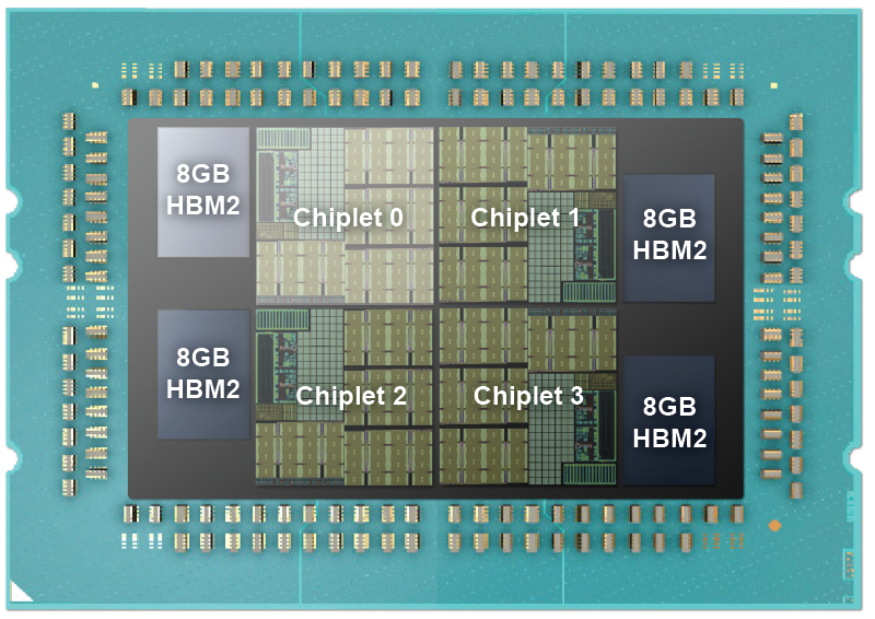
The proposed Manticore architecture consists of four () 22 nm chiplet dies on an interposer. Using chiplets improves yield and reduces cost. Each die has three short-range, multi-channel, in-package chip-to-chip links [8], one to each sibling. They are used for inter-die synchronization and chiplet-to-chiplet non-uniform memory access (NUMA). Furthermore, each chiplet has access to a private HBM. The conceptual floorplan is depicted in Figure 1.
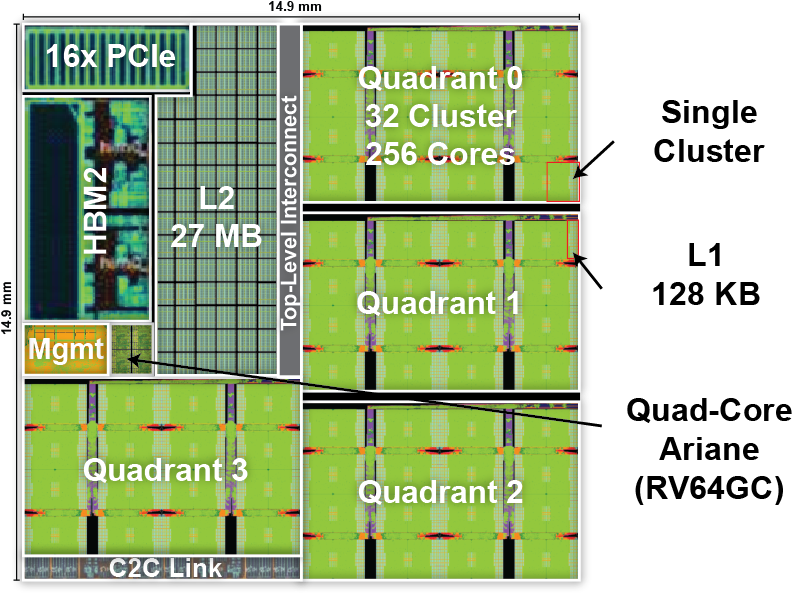
The chiplet (see Figure 2) contains four quadrants, consisting of 32 clusters with eight cores each, which results in 1024 cores for all four quadrants on a chiplet. Furthermore, each chiplet contains four Ariane RV64GC management cores [9] an HBM () controller, a of L2 memory, and a 16x PCIe endpoint () for host communication as shown in Figure 2.
The four Ariane management cores run a general-purpose operating system such as Linux and manage the Snitch clusters and program off-loading. The Manticore chiplet has enough silicon area to support on-chip shared L2 memory for critical data storage such as neural network weights or stencil kernels.
Memory Hierarchy
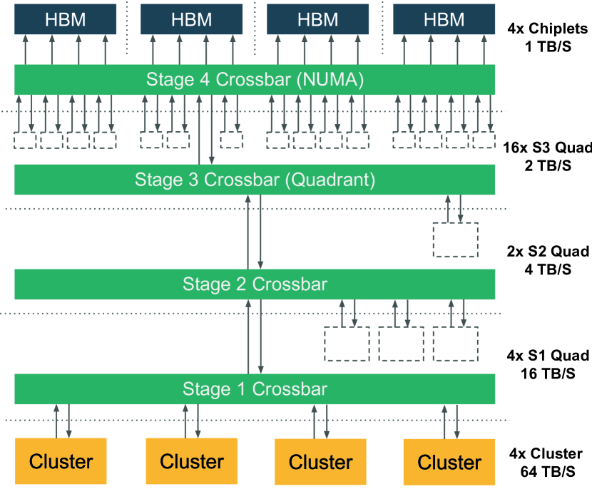
Each quadrant111The term quadrant is somewhat generic and does not necessarily imply four members (cores or lower stage quadrants), as the number of members can be adjusted to match the available bandwidth into the next stage, as for example, in stage three of our system (see Figure 3) is further subdivided into multiple stages, in a tree-structure using an interconnect tuned for burst-based direct memory transfer (DMA) accesses. Four clusters share an instruction cache and an uplink into the next stage. These four clusters have a high aggregate bandwidth of amongst each other and can perform low-latency, high-bandwidth intra-cluster data transfers. As shown in Figure 3, clusters share the uplink into the next higher stage, the bandwidth to the other S1 quadrants becomes smaller. Bandwidth is subsequently thinned as four S1 quadrants share an instruction cache and an uplink into the S2 quadrant and two S2 quadrants share an uplink into the S3 quadrant. In the last stage of hierarchy S3 quadrants, distributed over four chiplets (non-uniform memory access), share four HBMs with an aggregated peak bandwidth of . This bandwidth thinning scheme allows us to have a very low diameter, low latency interconnect topology, which can sustainably saturate the HBM bandwidth while being benign to floorplanning and physical design. The interconnect also allows for a very high cluster-to-cluster internal bandwidth, through multiple stages, which by far exceeds the bandwidth into the memory. With this model, we efficiently support cluster-to-cluster traffic, while, at the same time, fully loading the memory system.
Compute Cluster
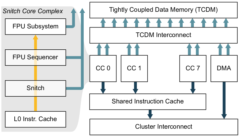
The compute cluster consists of eight small, , single-stage, 32 bit RISC-V processor cores [1] (see Figure 4). Each Snitch core contains a double-precision (DP) FPU, which can be used to compute one DP Fused Multiply-Add (FMA) operation or two SP FMAs per cycle. When running at , a cluster with eight Snitch cores is able to compute 16 DP or 32 SP flop, resulting in for the entire Manticore system. All eight cores have element-wise, low-latency, access into tightly coupled and shared scratchpad memory. Moreover, a DMA engine is in charge of moving blocks of data into the scratchpad memory over a 512 bit, data bus. The cores are clocked at , thus delivering more than peak compute per chiplet.
With this architecture, we achieve a very high compute/control ratio: of the system consisting of compute units, another spent on the L1 memory and just of the area are spent on the control parts.
Programming
We leverage two custom RISC-V ISA extensions to achieve extremely high FP utilization and efficiency: Xssr and Xfrep.
Stream Semantic Registers (Xssr)
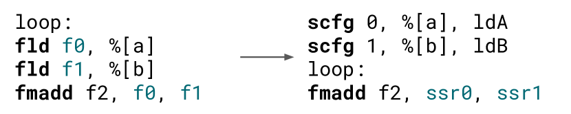
SSRs [2] offer a means to elide explicit load/store instructions in a program. This is achieved by giving a subset of the processor core’s registers stream semantics. When enabled, a read from such an SSR is translated in hardware into a load from memory, and conversely, a register write becomes a store to memory. Since an in-order single-issue core can only execute a single instruction every cycle, the presence of loads and stores in a hot loop of the program diminishes FPU utilization significantly. For example, consider a dot product, which has to issue two loads from memory for every FMA operation, as shown in Figure 5(a). In this scenario, even if the loop is fully unrolled, we achieve at most 33% FPU utilization. In theory, this allows the FPU to be 100% utilized, and even a simple processor can achieve >90% utilization in many relevant kernels without resorting to complex and energy-inefficient wide issue superscalar or very long instruction word (VLIW) architectures [2]. SSRs offer a way to elide memory accesses and address computation in hot loops, which in many cases leaves no integer instructions in the loop body.
Floating-Point Repetition (Xfrep)
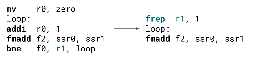
The FREP [1] extension implements a FPU-only hardware loop. Consider a dot product utilizing SSRs for example, as shown in Figure 5(b). Besides the essential FMA operation running on the FPU, the loop only consists of a trip count increment (addi) and a back-branch (bne). This loop can be replaced by a FREP instruction, which loops a range of subsequent FP instructions (one in this case) for a configurable number of times. The RISC-V ISA makes the integration of such an extension very straightforward as most instructions either operate entirely on integer or entirely on FP registers. Only a handful, such as comparisons or moves between integer and FP domains, exchange information from one domain to the other. We leverage this separation and insert a micro-loop sequence buffer of 16 instructions between the Snitch core and the FPU. FREP instructions configure this buffer to emit a range of buffered instructions multiple times into the FPU, which essentially implements the hardware loop. Since this happens entirely in the FPU subsystem outside of the Snitch core, the core’s integer pipeline can run in parallel, enabling a pseudo-dual-issue mode of operation that would not be achievable with a traditional hardware loop. This allows the core to perform non-trivial bookkeeping and address calculation while the FPU is running, without incurring a reduction of the FPU utilization.
Typical SSR/FREP Execution
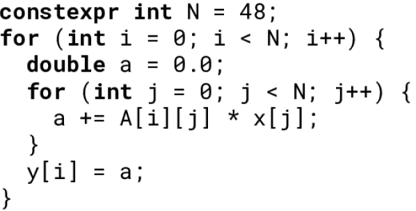
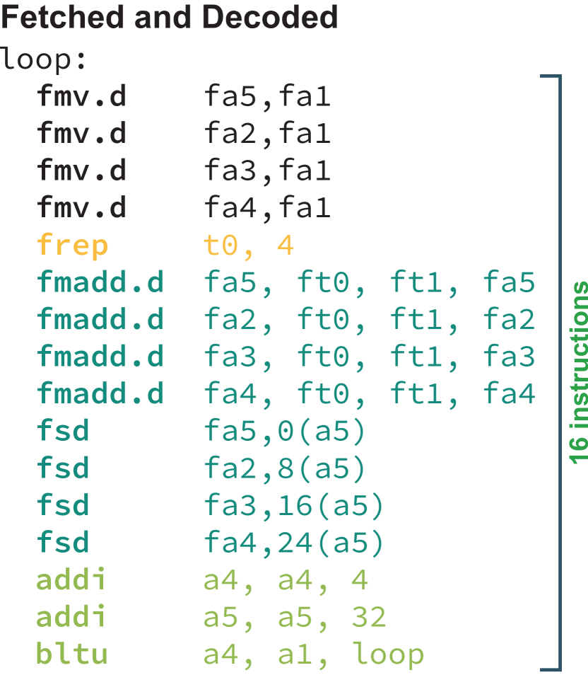
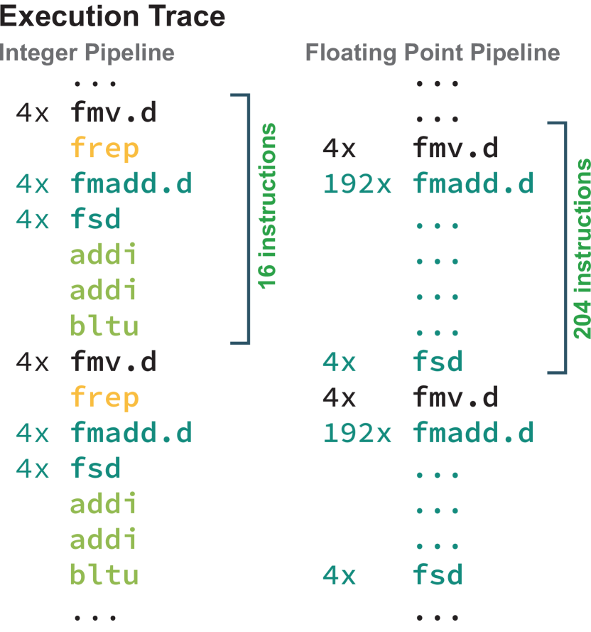
As a concrete example, let us consider the matrix-vector multiplication operation shown in Figure 6(a). A typical implementation leveraging Manticore’s SSR and FREP extensions is shown in Figure 6(b). The address computation and memory accesses of A and x are entirely performed by the SSRs ft0 and ft1. The inner loop is implemented using an FREP instruction and unrolled to compute four results in parallel in order to avoid pipeline stalls due to FPU latency. The outer loop is executed by the integer core. It stores the results (fsd), implements loop bookkeeping (addi, bltu), and initializes a (fmv.d).
As shown in Figure 6(c), the 16 instructions of the assembly implementation are fetched and decoded once by the integer pipeline of the processor core and expand to 204 executed instructions in the FPU through the use of FREP. This leaves 188 cycles for the integer pipeline for other tasks, such as preparing the next loop iteration or coordination of data movement. In case no other work is required, the 16 instructions fetched over 204 cycles of execution amounts to roughly one instruction every 13 cycles, mitigating the von Neumann bottleneck by reducing instruction fetch bandwidth by more than one order of magnitude. Since the FPU can execute the loop iterations back-to-back and of the 204 instructions, 192 perform actual computation, this kernel can achieve up to 94% FPU utilization.
Prototype
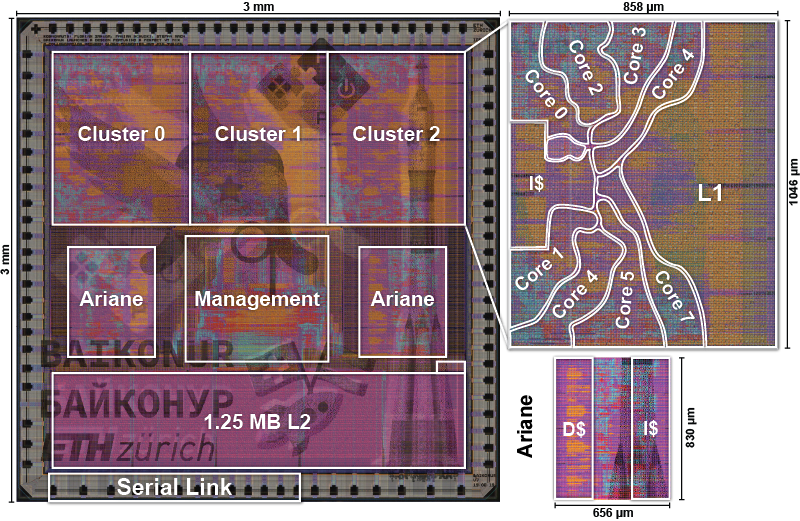
A prototype containing the logic core of the chiplet architecture was manufactured and characterized using the Globalfoundries 22FDX technology. The prototype in Figure 7 contains three Snitch clusters with eight cores (each configured with L1 instruction cache and L1 data memory organized in 32 banks), a dual-core Ariane (with L1 instruction cache and data cache), L2 memory, and a , double data-rate, , digital-only chip-to-chip link.
Silicon Performance
Efficiency
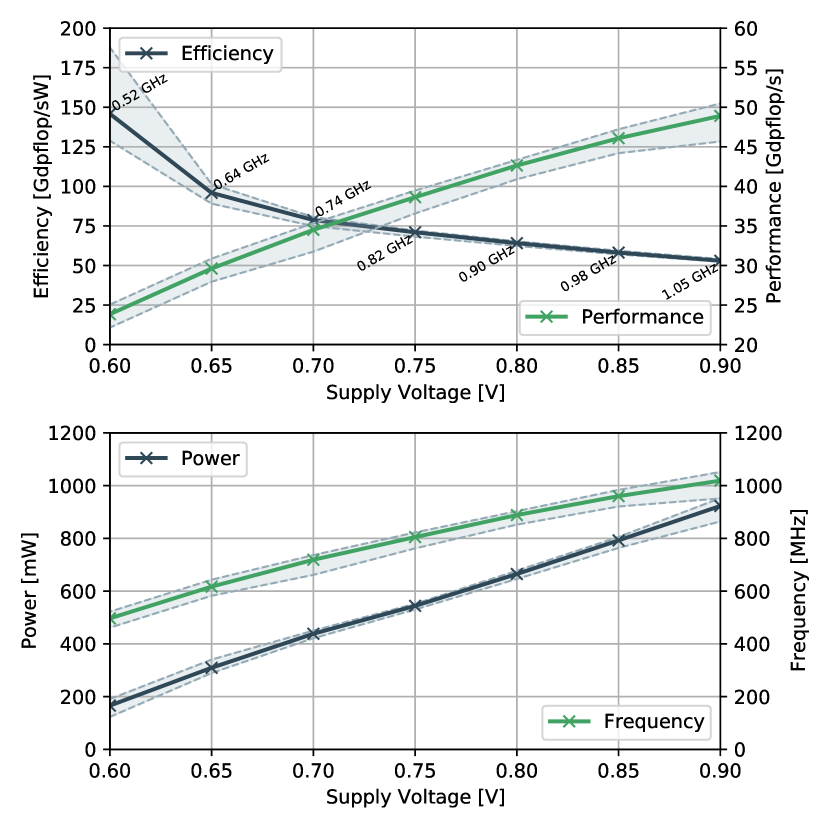
We measured the speed and power consumption of the prototype silicon under representative workloads and operating conditions. Figure 8 shows the DP performance and energy efficiency achieved when executing parallel workloads on the 24 cores of our prototype 22 nm silicon, for different operating voltages. The chips offer a wide range of operating points and choices for performance/efficiency trade-offs, which we leverage through dynamic voltage and frequency scaling (DVFS) based on the current workload’s operational intensity. This allows us to essentially adjust the roofline of the system to match the current workload. In high-performance mode running over at VDD, our architecture achieves a peak performance of across 24 cores and a compute density of up to , which translates to across a full 4096 cores. In max-efficiency mode running at at VDD, our architecture achieves an industry-leading efficiency of , while still delivering a respectable across 24 cores, which translates to across a full 4096 cores.
Roofline
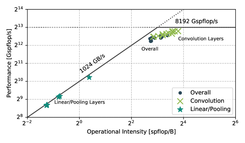
To assess the performance of the manufactured silicon, we analyzed workloads from training steps of a set of Deep Neural Networks (DNNs). Figure 9 shows the roofline plot of our architecture across a full training step. We estimate full-system performance based on cycle-accurate simulation of a smaller instantiation of the hardware, combined with an architectural model of the full system and measured performance characteristics of the prototype silicon. The compute-bound convolution layers in the workload reach >80% of the system’s peak performance, and the proximity to the point of inflection of the roofline indicates a balanced utilization of the hardware capabilities. The memory-bound linear and pooling layers reach >90% of the system’s peak bandwidth. Since DNN workloads tend to be dominated by the convolution layers, the overall performance, which considers all layers, is almost identical to the convolution performance. Overall we observe that the Manticore architecture is very efficient at tracking the performance and bandwidth roofline, with a detachment down to for low-intensity and for high-intensity optimized kernels. The worst-case detachment of from the roofline is encountered in the intermediate region around the point of inflection, where intuitively, the aggregate bandwidth pressure on the L1 TCDM is highest due to the DMA and the compute units both operating at capacity and banking conflicts more frequently stall L1 memory accesses.
Applications
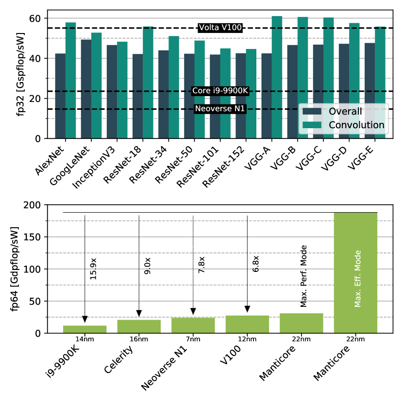
Figure 10 shows the SP energy efficiency achieved in a DNN training step overall, and on the compute-bound convolutions specifically, across a variety of networks, and the industry-leading DP efficiency on linear algebra. On SP DNN training workloads, Manticore’s actual efficiency is competitive with the V100 GPU’s peak efficiency and outperforms the Core i9-9900K CPU by 2 and the Neoverse N1 [10] by 3. On DP workloads, Manticore outperforms a V100 GPU’s peak efficiency by 6, the N1 by 7, the Celerity RISC-V CPU by 9, and the Core i9-9900K CPU by 15. Our architecture achieves this despite these chips having a substantial technology advantage due to their 7 nm, 12 nm, and 14 nm FinFET processes. Regarding the A100 GPU, our initial estimates based on data published by Nvidia [7] suggest that it achieves a 25% improvement on SP and DP over the V100 in terms of speed at similar power consumption. This indicates that Manticore has just 25% lower efficiency on SP than A100, but outperforms it on DP by 5, despite the A100’s significant 7 nm FinFET technology advantage. Manticore delivers significantly higher peak FP performance than comparable RISC-V architectures [11] in 16 nm.
Acknowledgment
This project was supported in part by the European Union’s H2020 program grant agreement numbers 826647 (European Processor Initiative-EPI) and 732631 (Open Transprecision Computing - "OPRECOMP").
References
- [1] F. Zaruba, F. Schuiki, T. Hoefler, and L. Benini, “Snitch: A tiny Pseudo Dual-Issue Processor for Area and Energy Efficient Execution of Floating-Point Intensive Workloads,” IEEE Transactions on Computers, 2020.
- [2] F. Schuiki, F. Zaruba, T. Hoefler, and L. Benini, “Stream Semantic Registers: A Lightweight RISC-V ISA Extension Achieving Full Compute Utilization in Single-Issue Cores,” IEEE Transactions on Computers, 2020.
- [3] “AI and Compute,” [Online] https://openai.com/blog/ai-and-compute/, 2020, Accessed: 2020-05-10.
- [4] N. P. Jouppi, D. H. Yoon, G. Kurian, S. Li, N. Patil, J. Laudon, C. Young, and D. Patterson, “A domain-specific supercomputer for training deep neural networks,” Communications of the ACM, 2020.
- [5] A. Yang, “Deep Learning Training At Scale Spring Crest Deep Learning Accelerator,” in Hot Chips: A Symposium on High Performance Chips, vol. 31. IEEE Computer Society, 2019.
- [6] T. Yoshida, “Fujitsu high performance CPU for the Post-K Computer,” in Hot Chips: A Symposium on High Performance Chips, vol. 30. IEEE Computer Society, 2018.
- [7] NVIDIA, “NVIDIA Ampere GA102 GPU Architecture - The Ultimate Play,” 2020.
- [8] P. Vivet and et.al., “A 220GOPS 96-core Processor with 6 Chiplets 3D-stacked on an Active Interposer Offering 0.6ns/mm Latency, 3TBit/s/mm2 inter-Chiplet Interconnects and 156mW/mm2@82% Peak-Efficiency DC-DC Converters,” Solid-State Circuits (ISSCC), IEEE International Conference, 2020.
- [9] F. Zaruba and L. Benini, “The Cost of Application-class Processing: Energy and Performance Analysis of a Linux-ready 1.7-GHz 64-bit RISC-V core in 22-nm FDSOI Technology,” IEEE Transactions on Very Large Scale Integration (VLSI) Systems, vol. 27, no. 11, 2019.
- [10] R. Christy, S. Riches, S. Kottekkat, P. Gopinath, K. Sawant, A. Kona, and R. Harrison, “A 3GHz Arm Neoverse N1 CPU in 7nm FinFet for infrastructure applications,” Solid-State Circuits (ISSCC), IEEE International Conference, 2020.
- [11] S. Davidson, S. Xie, C. Torng, K. Al-Hawai, A. Rovinski, T. Ajayi, L. Vega, C. Zhao, R. Zhao, S. Dai et al., “The Celerity open-source 511-core RISC-V tiered accelerator fabric: Fast architectures and design methodologies for fast chips,” IEEE Micro, vol. 38, no. 2, 2018.
Florian Zaruba received his BSc degree from TU Wien in 2014 and his MSc from the Swiss Federal Institute of Technology Zurich in 2017. He is currently pursuing a PhD degree with the Digital Circuits and Systems group of Luca Benini. Contact him at zarubaf@iis.ee.ethz.ch.
Fabian Schuiki received his BSc and MSc degree in electrical engineering from ETH Zürich, in 2014 and 2016, respectively. He is currently pursuing a PhD degree with the Digital Circuits and Systems group of Luca Benini. Contact him at fschuiki@iis.ee.ethz.ch.
Luca Benini holds the Chair of Digital Circuits and Systems at ETHZ and is Full Professor at the Universita di Bologna. He is a Fellow of the ACM and a member of the Academia Europaea. Contact him at lbenini@iis.ee.ethz.ch.