Direct quantification of topological protection in symmetry-protected photonic edge states at telecom wavelengths
Abstract
Topological on-chip photonics based on tailored photonic crystals (PhC) that emulate quantum valley Hall effects has recently gained widespread interest due to its promise of robust unidirectional transport of classical and quantum information. We present a direct quantitative evaluation of topological photonic edge eigenstates and their transport properties in the telecom wavelength range using phase-resolved near-field optical microscopy. Experimentally visualizing the detailed sub-wavelength structure of these modes propagating along the interface between two topologically non-trivial mirror-symmetric lattices allows us to map their dispersion relation and differentiate between the contributions of several higher-order Bloch harmonics. Selective probing of forward and backward propagating modes as defined by their phase velocities enables a direct quantification of topological robustness. Studying near-field propagation in controlled defects allows to extract upper limits to topological protection in on-chip photonic systems in comparison to conventional PhC waveguides. We find that protected edge states are two orders of magnitude more robust than the latter. This direct experimental quantification of topological robustness comprises a crucial step towards the application of topologically protected guiding in integrated photonics, allowing for unprecedented error-free photonic quantum network
The emergence of photonic topological insulators (PTIs) has led to promising theoretical and experimental approaches for topology-protected light-matter interaction Klembt et al. (2018) and integration of robust quantum devices Carusotto and Ciuti (2013). Topologically protected photonic edge states offer robust energy transport with unprecedented guiding capabilities, providing a cornerstone for efficient distribution of classical and quantum information in dense networks Hasan (2010); Wang et al. (2008). The notion of such states supporting unhindered transport around defects and sharp corners is especially interesting for on-chip applications. In addition to Chern-type PTIs that break time-reversal symmetry Haldane and Raghu (2008); Raghu and Haldane (2008); Wang et al. (2008); Plotnik et al. (2014), a time-reversal invariant realization of lossless optical transport was introduced theoretically on a dielectric photonic crystal (PhC) platform at telecom frequencies Wu and Hu (2015); Khanikaev et al. (2013). While the existence of these states has been evidenced in the linear Barik et al. (2018); Parappurath et al. (2020) and nonlinear regime Smirnova et al. (2019), and topological robustness has been inferred by high transmission Shalaev et al. (2019); He et al. (2019), quantifying their defining quality of scattering-free propagation has remained elusive. Potential interference effects and out-of-plane scattering losses at local disorder render such a quantification challenging. Here, we report a rigorous robustness evaluation of valley photonic edge eigenstates at telecom wavelengths. Local investigation of the states’ transport properties via phase-resolving near-field microscopy gives direct insight into topological protection, through distinction between forward and backward waves. We find that protected edge states are two orders of magnitude more robust as compared to conventional waveguides. This determination of significantly suppressed back-reflection provides a crucial step towards implementing topological guiding in on-chip photonic networks.
We realize valley-Hall PhCs (VPCs), which rely on the valley degree of freedom linked to the breaking of a specific lattice symmetry Shalaev et al. (2019); Lu et al. (2014, 2018); Kim et al. (2014); Dubrovkin et al. (2020). Similar to the valley-selective polarization caused by spin-orbit coupling in transition metal dichalcogenides Dong et al. (2017), these PhC lattices exhibit a non-vanishing Berry curvature at the and points of the Brillouin zone Tzuhsuan and Shvets (2016). Since each valley is associated with an intrinsic magnetic moment, the valley-Chern invariant signifies a pseudo-spin Xiao et al. (2007), rendering the bulk band structure topologically non-trivial. A domain wall formed by two parity inverted copies of the PhC lattice results in two degenerate and robust edge-state eigenmodes confined to the interface that linearly traverse the photonic band gap (PBG), each with a unique pseudo-spin Zak (1989). As long as the lattice symmetry is preserved and no inter-valley scattering occurs to flip the pseudo-spin, these edge states are predicted to be immune to reflection from local disorder along the domain wall Tzuhsuan and Shvets (2016); Cheng et al. (2016).
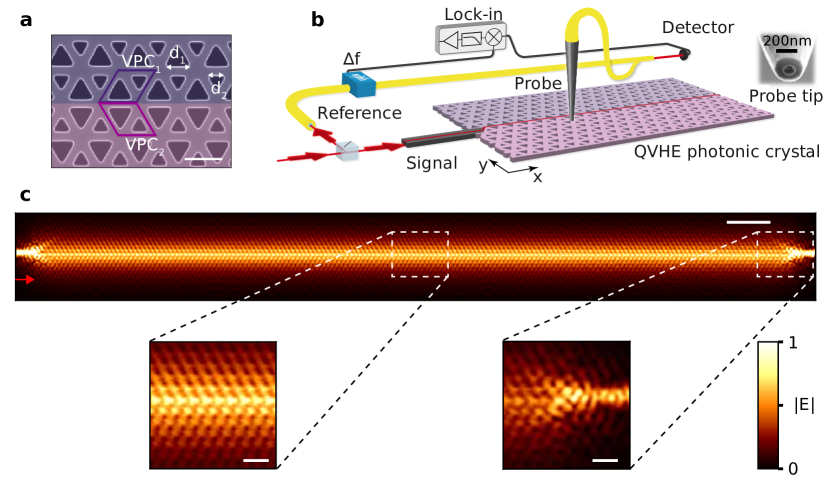
To determine the experimentally achievable robustness against back-scattering, we fabricate a VPC working at telecom wavelengths on a silicon-on-insulator (SOI) platform following the design of Shalaev et al. (2019) (see Fig. 1a). Light is coupled into the PhC structure in the + direction from an access waveguide. This system supports edge modes of opposite group velocity (see Supplementary Fig. S1) propagating along the domain wall between two parity-transformed lattices (VPC1 and VPC2). We visualize the spatial wavefunction of the mode with a phase-sensitive near-field scanning optical microscope (NSOM) (Fig. 1b) Gersen et al. (2005); Rotenberg and Kuipers (2014). Figure 1c shows the measured two-dimensional in-plane field amplitude map at a wavelength of . The detected transverse-electric (TE)-like field pattern confined to the interface of VPC1 and VPC2 extends laterally over roughly five unit cells, revealing an intricate sub-wavelength mode structure (left inset of Fig. 1c). The measured fields show close correspondence to numerical calculations (see Supplementary Fig. S1). At the locations of the access and exit waveguide, the influence of broken lattice symmetry and the adjacent feed waveguide becomes evident in the distorted field pattern (right inset of Fig. 1c).
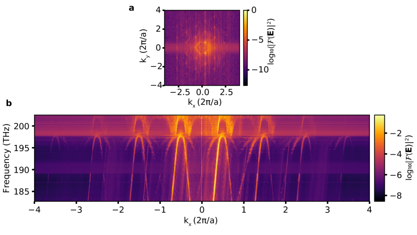
The heterodyne detection configuration of the employed NSOM gives access to the complex in-plane optical fields of the edge mode Balistreri et al. (2000). As a direct consequence of Bloch’s theorem, the two-dimensional spatial Fourier transformation of the measured field amplitude allows individual analysis of Fourier components with positive and negative phase velocities. An illustrative Fourier map at is displayed in Fig. 2a. By repeating the near-field scans and corresponding Fourier analysis for and integrating over , we extract the mode dispersion shown in Fig. 2b. We resolve at least six parallel lines due to the excellent signal to background ratio (S/B) of . The achieved spatial resolution, combined with the high S/B, enables us to resolve higher-order Bloch harmonics over multiple Brillouin zones. The lines with a positive slope correspond to a single forward-propagating mode with group velocity . Closer inspection reveals negatively-sloped lines corresponding to a single backward propagating mode with Engelen et al. (2007); Burresi et al. (2009). This separation of forward- and backward-propagating Bloch modes allows local monitoring of back-scattering along the domain wall.
Using this local phase and amplitude information, we probe a straight edge domain wall shown in Fig. 1c. We obtain the quantities and representing the forward and backward energy, respectively, through integration of their corresponding Fourier intensity. The ratio unambiguously yields the conversion from forward to backward propagation, a result of scattering events occurring at and beyond the VPC end facet. Thus, includes coupling of the forward to backward mode energy away from the topologically protected regime. This initial examination of the straight edge with the observed back-propagation energy dominated by contributions of the end-facet, calls for a more intricate analysis of topological protection.
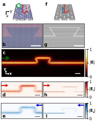
To quantify protection without the aforementioned contributions, we introduce a trapezoidal (-shaped) structure along the domain wall comprising four sharp corners (Fig. 3). This structure is expected to be topologically-protected since bends respect the underlying lattice symmetry. Reflections characterized by energy coupled between the degenerate forward () and backward () propagating modes are indicated by red and blue arrows, respectively, in the schematic Fig. 3a. Figure 3c shows a map of the measured amplitude of the VPC edge mode. Separating the forward and backward modes through Fourier filtering leads to Fig. 3d and e. Figure 3d qualitatively demonstrates that the forward propagating mode exhibits a near-unity transmission through the bend. The constant amplitude of the backward propagating mode (Fig. 3e) also indicates near-unity transmission. This demonstrates that we may attribute the coupling of the forward and the backward mode to the termination of the exit PhC waveguide. Put differently, light is perfectly guided around the -shaped domain wall, with the transmission being independent of the presence of the defect itself.
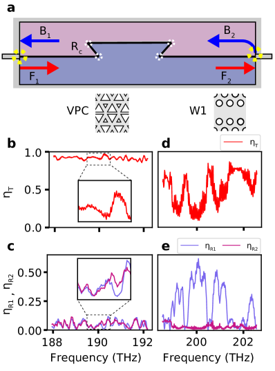
This observation is quantified by translating the locally measured amplitudes into mode energy ratios. We filter the Fourier intensity distribution to obtain the forward and backward propagating mode energy before () and after () the -bend (see Fig. 4a). Locally determined transmission through the defect for the linear part of the dispersion is shown in Fig. 4b. A mean transmission value of is obtained for the chosen frequency range. Additionally, the mode energy ratios calculated for regions before () and after () the defect are shown for a frequency range of in Fig. 4c. We notice that () and () are almost indistinguishable. This strongly suggests that the contribution of the four symmetry-protected corners to the back-propagation energy is insignificant with respect to back-scattering at the end facet.
Although expected, one can appreciate that the remarkably large transmission over the mode’s full frequency range Ma et al. (2015); He et al. (2019); Tzuhsuan and Shvets (2016) is reasonably atypical in comparison with a topologically trivial standard “W1” PhC waveguide (see Methods for fabrication details). We again introduce a trapezoidal structure in said PhC waveguide (Fig. 3f, g). It is worth mentioning that the fabricated W1 waveguide corners are not optimised for unity transmission at any given frequency Krauss et al. (2010). In stark contrast to the forward and backward mode for a VPC (Fig. 3d, e), the W1 modes (Fig. 3h, i) show significant loss across the defect. Moreover, the normalized backward amplitude map in Fig. 3i demonstrates that the dominant reflections already occur at the first corner. The mode energy here is converted to a back-reflected wave and additionally experiences out-of-plane scattering loss. The measured through the -structure in the W1 PhC, shown in Fig. 4d, is on average one-third of the observed for the VPC. The strong reflection from the first corner is confirmed by shown in Fig. 4e, where is four times higher than for certain frequencies in the W1 PhC waveguide.
In addition to the back-reflection from the individual corners, the direct evaluation of the -shaped defect is affected by other aspects: out-of-plane scattering losses, scattering at the end-facet and interference due to multiple reflections along the domain wall. We notice rapid oscillations in before and after the defect (Fig. 4c,e). To disentangle the back-scattering contribution from the aforementioned effects, we consider the complex scalar mode amplitude of the Bloch wave at different points along the domain wall. With the assumption of a perfectly mirror symmetric device, we treat the defect as a single effective interface in a transfer-matrix model (TMM). Using and as input parameters to the model, we quantify the mean reflectance of the full defect. Details of the model and the precise extraction method can be found in the Supplementary Sec. II. Applying the model to the data for the topologically protected edge states shown in Fig. 4b,c we retrieve a mean effective reflectance for the full defect and an out-of-plane scattering loss for the topologically protected edge states. Furthermore, we determine the average single-corner reflectance from the TMM (see Supplementary Sec.II C).
The same approach applied to the data in Fig. 4d,e for the W1 PhC waveguide reveals a reflectance of , two orders of magnitude larger than that observed for the VPC, and an out-of-plane scattering coefficient . These values for the W1 structure are in close agreement with literature Kuang and O’Brien (2004); Chow et al. (2001); Chutinan et al. (2002). A topologically protected PhC lattice thus reduces the experimentally achievable back-reflection from individual sharp corners by two orders of magnitude over the entire frequency range of the edge state.
In summary, a direct experimental quantification of topological protection in VPC-based PTIs at telecom frequencies was achieved by accessing the full complex wavefunction of the edge state via phase-resolved near-field microscopy. This allows for determination of back-reflection from topologically protected defects as well as for quantification of the experimentally unavoidable out-of-plane scattering losses. We unambiguously determined an experimental upper limit to the back-scattering contribution from symmetry-protected defects in PhC-based topological edge states. This evaluation opens a direct pathway towards applied quantum topological photonic networks for secure and robust communications.
References
- Klembt et al. (2018) S. Klembt, T. H. Harder, O. A. Egorov, K. Winkler, R. Ge, M. A. Bandres, M. Emmerling, L. Worschech, T. C. Liew, M. Segev, C. Schneider, and S. Höfling, Nature 562, 552 (2018).
- Carusotto and Ciuti (2013) I. Carusotto and C. Ciuti, Reviews of Modern Physics 85, 299 (2013).
- Hasan (2010) M. Z. Hasan, Review of Modern Physics 82, 3045 (2010).
- Wang et al. (2008) Z. Wang, Y. D. Chong, J. D. Joannopoulos, and M. Soljačić, Physical Review Letters 100, 013905 (2008).
- Haldane and Raghu (2008) F. D. M. Haldane and S. Raghu, Physical Review Letters 100, 013904 (2008).
- Raghu and Haldane (2008) S. Raghu and F. D. Haldane, Physical Review A 78, 033834 (2008).
- Plotnik et al. (2014) Y. Plotnik, M. C. Rechtsman, D. Song, M. Heinrich, J. M. Zeuner, S. Nolte, Y. Lumer, N. Malkova, J. Xu, A. Szameit, Z. Chen, and M. Segev, Nature Materials 13, 57 (2014).
- Wu and Hu (2015) L. H. Wu and X. Hu, Physical Review Letters 114, 223901 (2015).
- Khanikaev et al. (2013) A. B. Khanikaev, S. Hossein Mousavi, W. K. Tse, M. Kargarian, A. H. MacDonald, and G. Shvets, Nature Materials 12, 233 (2013).
- Barik et al. (2018) S. Barik, A. Karasahin, C. Flower, T. Cai, H. Miyake, W. DeGottardi, M. Hafezi, and E. Waks, Science 359, 666 (2018).
- Parappurath et al. (2020) N. Parappurath, F. Alpeggiani, L. Kuipers, and E. Verhagen, Science Advances 6, eaaw4137 (2020).
- Smirnova et al. (2019) D. Smirnova, S. Kruk, D. Leykam, E. Melik-Gaykazyan, D. Y. Choi, and Y. Kivshar, Physical Review Letters 123, 103901 (2019).
- Shalaev et al. (2019) M. I. Shalaev, W. Walasik, A. Tsukernik, Y. Xu, and N. M. Litchinitser, Nature Nanotechnology 14, 31 (2019).
- He et al. (2019) X. T. He, E. T. Liang, J. J. Yuan, H. Y. Qiu, X. D. Chen, F. L. Zhao, and J. W. Dong, Nature Communications 10, 872 (2019).
- Lu et al. (2014) L. Lu, J. D. Joannopoulos, and M. Soljačić, Nature Photonics 8, 821 (2014).
- Lu et al. (2018) M.-H. Lu, Z. D. Wang, H.-F. Wang, B.-Y. Xie, X.-Y. Zhu, and Y.-F. Chen, Optics Express 26, 24531 (2018).
- Kim et al. (2014) Y. Kim, K. Choi, J. Ihm, and H. Jin, Physical Review B 89, 085429 (2014).
- Dubrovkin et al. (2020) A. M. Dubrovkin, U. Chattopadhyay, B. Qiang, O. Buchnev, Q. J. Wang, Y. Chong, and N. I. Zheludev, Applied Physics Letters 116, 191105 (2020).
- Dong et al. (2017) J. W. Dong, X. D. Chen, H. Zhu, Y. Wang, and X. Zhang, Nature Materials 16, 298 (2017).
- Tzuhsuan and Shvets (2016) M. Tzuhsuan and G. Shvets, New Journal of Physics 18, 25012 (2016).
- Xiao et al. (2007) D. Xiao, W. Yao, and Q. Niu, Physical Review Letters 99, 236809 (2007).
- Zak (1989) J. Zak, Physical Review Letters 62, 2747 (1989).
- Cheng et al. (2016) X. Cheng, C. Jouvaud, X. Ni, S. H. Mousavi, A. Z. Genack, and A. B. Khanikaev, Nature Materials 15, 542 (2016).
- Gersen et al. (2005) H. Gersen, T. J. Karle, R. J. P. Engelen, W. Bogaerts, J. P. Korterik, N. F. van Hulst, T. F. Krauss, and L. Kuipers, Phys Rev Lett 94, 123901 (2005).
- Rotenberg and Kuipers (2014) N. Rotenberg and L. Kuipers, Nature Photonics 8, 919 (2014).
- Balistreri et al. (2000) M. L. M. Balistreri, J. P. Korterik, L. Kuipers, and N. F. van Hulst, Physical Review Letters 85, 294 (2000).
- Engelen et al. (2007) R. J. Engelen, Y. Sugimoto, H. Gersen, N. Ikeda, K. Asakawa, and L. Kuipers, Nature Physics 3, 401 (2007).
- Burresi et al. (2009) M. Burresi, R. J. Engelen, A. Opheij, D. Van Oosten, D. Mori, T. Baba, and L. Kuipers, Physical Review Letters 102, 033902 (2009).
- Ma et al. (2015) T. Ma, A. B. Khanikaev, S. H. Mousavi, and G. Shvets, Physical Review Letters 114, 127401 (2015).
- Krauss et al. (2010) T. F. Krauss, L. O’Faolain, S. Schulz, D. M. Beggs, F. Morichetti, A. Canciamilla, M. Torregiani, A. Melloni, S. Mazoyer, P. Lalanne, A. Samarelli, M. Sorel, and R. De La Rue, Advances in Slow and Fast Light III 7612, 76120L (2010).
- Kuang and O’Brien (2004) W. Kuang and J. D. O’Brien, OSA Trends in Optics and Photonics Series 96 A, 1497 (2004).
- Chow et al. (2001) E. Chow, S. Y. Lin, J. R. Wendt, S. G. Johnson, and J. D. Joannopoulos, Optics Letters 26, 286 (2001).
- Chutinan et al. (2002) A. Chutinan, M. Okano, and S. Noda, Applied Physics Letters 80, 1698 (2002).
- Johnson and Joannopoulos (2001) S. Johnson and J. Joannopoulos, Optics Express 8, 173 (2001).
I Methods
Simulations. Numerical simulations were performed using MIT Photonic Bands Johnson and Joannopoulos (2001) with the in-plane field distributions and retrieved dispersion relation shown in the supplementary materials. To match the calculated edge state to the measured dispersion relation, the refractive index of silicon was chosen as . In order to account for the corner roundness arising from fabrication, a fillet of radius was added to the triangular holes of lattice constant . The unit cell consisted of equilateral triangles, with a larger triangle side length and smaller triangle side length . In addition, finite-difference time-domain calculations (FDTD Solutions by Lumerical) were used to verify the intrinsic transmittance spectra through bends in a W1 PhC waveguide.
Device fabrication. The PhC slab was fabricated on a silicon-on-insulator (SOI) platform with a thick silicon layer on a buried oxide layer. The fabrication was performed in two steps: First, a positive electron-beam resist of thickness (AR-P 6200.09) was spin-coated between a monolayer of adhesion reagent HMDS and a conductive layer of E-Spacer 300Z. Then, the PhC design was patterned in the resist using e-beam lithography on a Raith Voyager with beam exposure. The e-beam resist was developed in pentyl acetate/O-Xylene/MIBK:IPA(9:1)/isopropanol, and the SOI chip subsequently underwent reactive-ion etching in HBr and O2. In a second step, the photo-lithography resist AZ1518 was patterned using a Suss MABA6 Mask Aligner to define a selective wet-etching window on the PhC. After development with AZ400K:H2O, the buried-oxide layer was removed in an aqueous 5:1 solution of hydrofluoric acid. The PhC was then subjected to critical point drying before being mounted in the near-field optical microscopy setup. The PhCs are terminated on both sides such that a TE single-mode Si-ridge waveguide is extended as PhC waveguide into the crystal to enable better index-matching for efficient incoupling Shalaev et al. (2019).
The PhC lattice features a honeycomb configuration of two equilateral triangles in a unit cell of lattice constant . One triangle is scaled up () and the other down (), while preserving lattice symmetry. A domain wall is created along the VPC1 and VPC2 by applying a parity operation along the spatial -coordinate. Two different VPC domain walls were fabricated to facilitate transmission and back-scattering comparisons. The straight edge VPC has dimensions designed such that the PBG falls within the tunable laser wavelength range of . For the trapezoidal edge VPC domain wall, the two diagonals extend over unit cells, whereas the horizontal extent of the defect between the second and third corner is unit cells.
The standard ‘W1’ waveguide is formed from a honeycomb lattice of circular holes, with a lattice constant of and hole radius , where one row of circular holes was removed.
Near-field optical microscopy setup. The utilized aperture-based near-field optical microscope consists of a tapered optical fiber coated homogeneously with aluminium. An aperture of ca. is created at its apex via focused ion beam milling. Scanning the probe over the silicon membrane at a relative height of controlled via shear force feedback results in the pickup of the local in-plane field components. Their amplitudes and phases are determined using a heterodyne detection scheme, with the coherent reference light beam shifted by in frequency Rotenberg and Kuipers (2014).
II Acknowledgements
We thank Nikhil Parappurath, Filippo Alpeggiani and Aron Opheij for fruitful discussions about the initial design, fabrication and measurement steps. This work is part of the research programme of the Netherlands Organisation for Scientific Research (NWO). The authors acknowledge support from the European Research Council (ERC) Advanced Investigator Grant no. 340438-CONSTANS and ERC starting grant no. 759644-TOPP.
III Author Contributions
R.B. fabricated the devices. S.A. and T.B. carried out the near-field measurements. S.A, R.B. and T.B. performed data analysis and modelling. E.V. and L.K. conceived and supervised the project. All authors contributed extensively to the interpretation of results and writing of the manuscript.
IV Data availability
All data obtained in the study are available from the corresponding author upon reasonable request.