Observation of Distinct Superconducting Phases in Hyperdoped p-type Germanium
Realization of superconductivity in Group IV semiconductors could have a strong impact in the direction quantum technologies will take in the future. Therefore, it is imperative to understand the nature of the superconducting phases in materials such as Silicon and Germanium. Here, we report systematic synthesis and characterization of superconducting phases in hyperdoped Germanium prepared by Gallium ion implantation beyond its solubility limits. The resulting structural and physical characteristics have been tailored by changing the implantation energy and activation annealing temperature. Surprisingly, in addition to the poly-crystalline phase with weakly-coupled superconducting Ga clusters we find a nano-crystalline phase with quasi-2D characteristics consisting of a thin Ga film constrained near top surfaces. The new phase shows signatures of strong disorder such as anomalous B temperature dependence and crossings in magentoresistance isotherms. Apart from using hyperdoped Ge as a potential test-bed for studying signatures of Quantum phase transitions (e.g. quantum Griffith singularity), our results suggest the possibility of integration of hyperdoped Ge nano-crystalline phase into superconducting circuits due to its 2D nature.
Introduction
The last decade has witnessed significant advances in the materials synthesis for superconducting circuits. Amongst them, superconductors–semiconductor (S-Sm) hybrid materials platforms have attracted a great deal of attention. For instance, many exciting avenues, built upon the success of gate-tunable hybrid epitaxial Al–InAs Josephson junctions technology 1; 2; 3, have been explored including gate-tunable transmon qubits 4, gate-tunable quantum busses 5, and platforms for superconducting spintronics and topological superconducting qubits 6; 7; 8. However, Group IV semiconductors are of particular interest for integration into Sm-S platforms due to their high purity and compatibility with highly scalable complimentary metal-oxide-semiconductor (CMOS) technologies 9; 10. Realization of superconductivity by hyperdoping is believed to facilitate such integration. So far, superconductivity has been successfully documented for diamond 11; 12, Silicon 13; 14; 15 and Germanium 16; 17 by hyperdoping with acceptors (i.e. B and Ga). The high doping levels are expected to surpass the metal–insulator transition limits, leading to a narrower band gap and larger inter-valley coupling 18; 19.
Germanium (Ge) is a compelling candidate for S-Sm platforms because ultra-clean materials with high hole mobilities may be achieved 20. In its pure and alloyed state, Ge is used in a wide variety of room-temperature electronics with high integrability with Si technology. Superconductivity in Ge is demonstrated through Ga+ ion implantation followed by dopant activation via rapid thermal annealing (RTA) or flash lamp annealing (FLA) at temperatures near the Ge melting point () 21; 16; 22; 23. Such high temperatures were intended for recovering the crystallinity of the Ge substrate damaged by implantation. Nevertheless, given its low solubility in Ge (maximum of 1.1% at about 700 ∘C 24), Ga is expected to not only take interstitial sites, but to segregate into clusters within the bulk or accumulate near the top surfaces. While such phase may not be thermodynamically stable, rapid cooling after annealing could help them reside within the implanted regions as metastable phases.
In this work, we show the possibility to tune the superconducting properties of hyperdoped Ge using two major processing parameters: 1) Ga+ implantation energy (EIMP); 2) dopant activation anneal temperature (TDA). We show superconductivity in hyperdoped Ge over a wide parameter space with EIMP and TDA as low as 25 keV and 350 ∘C, respectively. In this extended parameter space, two structurally and physically distinct phases are identified, namely the poly-crystalline (PC) and the nano-crystalline (NC) phases. The PC phase has low critical magnetic fields (Bc) with a 3D network of coupled superconducting Ga puddles 27. Conversely, the NC phase superconductivity, stemming from Ga thin film accumulated near the SiO2/Ge interface, can survive in-plane fields as high as 8 T. Interestingly, samples from both PC and NC phases are found to have anomalous temperature dependence of Bc as T0, pointing to the presence of quenched disorder and vortex glass state 28. Moreover, clear crossing zones are identified for sheet resistance, Rs(B), curves in 2D NC phases, offering the possibility of using this system to study properties of quantum critical point (QCP), and in general quantum phase transitions (QPTs) 29; 30. Signatures of high disorder could be applicable to quantum circuits where high kinetic inductance is needed. This could invoke a range of applications as in superinductors 31, magnetic-field-resistant superconducting resonators 32; 33 and phase slip qubits 34; 35.
Results
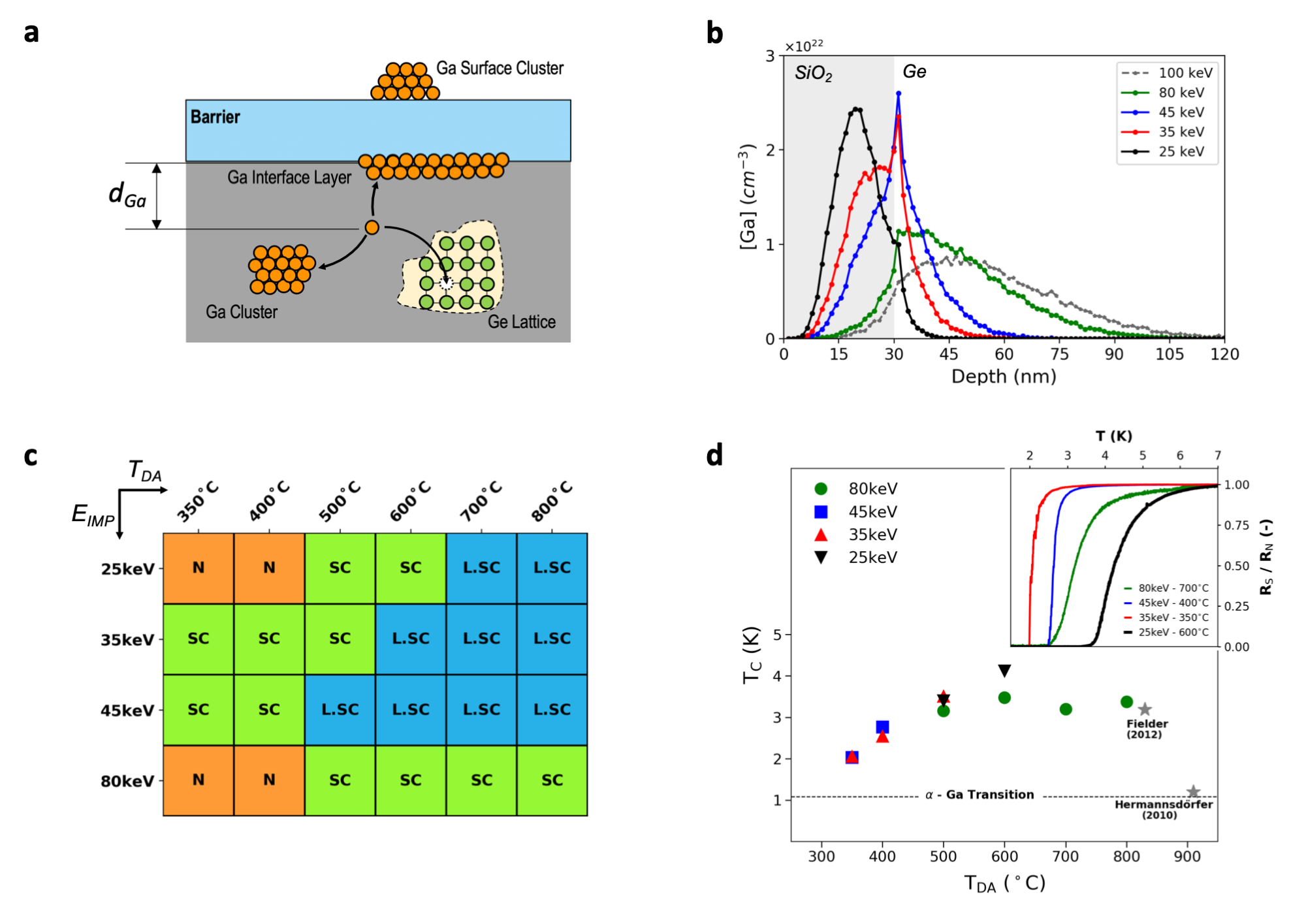
Transport properties vs. processing conditions. Figure 1a displays the pathways Ga ions may take within the Ge substrate during the activation annealing. In this picture, an oxide barrier is depicted on top of the Ge substrate, as it is commonly used to prevent surface damage during the ion implantation process. Due to low solubility, beside being incorporated into the bulk Ge lattice as a dopant, Ga could segregate into clusters within the implanted region, form a thin layer at the Ge/barrier interface or even diffuse through the barrier to form surface droplets. The percentage of Ga atoms participating in each process depends on the average distance of the implanted atoms from the top surface as well as the amount thermal energy provided during the annealing. Figure 1b shows the Ga distribution as a function of EIMP, simulated using the Transport of Ions In Matter (TRIM) Monte Carlo software 36. The lines show Ga concentration (per cm3) vs. depth for EIMP = 25, 35, 45, and 80 keV all experimentally implemented in this study. The grey line represents Ga distribution for EIMP = 100 keV, serving as a reference to the previous reports on superconducting Ge 21; 16; 37.
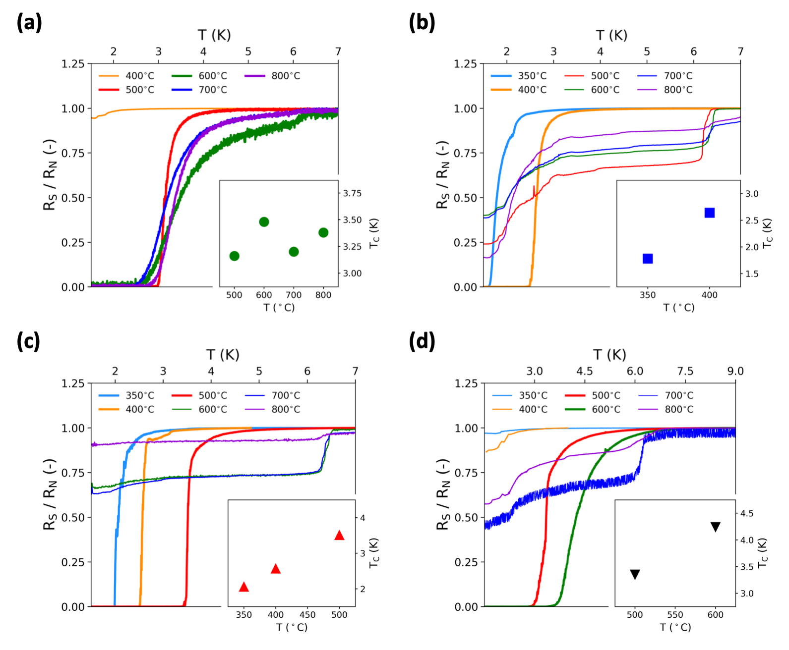
Implanted samples underwent RTA for 1 min in order to partially recover the crystal structure and to incorporate Ga atoms into interstitial sites as acceptors. RTA was carried out in a wide temperature range from 300 ∘C to 800 ∘C. Figure 1c shows a matrix of EIMP vs. TDA for the Ga-implanted Ge samples prepared in this study. The boxes labeled by ”SC” signify samples with clear superconducting transitions to a zero-resistance phase (see inset of 1d). Samples labeled with ”N” showed non-zero resistance all the way down to 1.5 K in the absence of any distinctive superconducting transition above that temperature. Finally, samples labeled by ”L.SC” that stands for localized superconductivity displayed a clear drop in resistance at 5–7 K, yet finite resistance at 1.5 K (see supplementary figure S1). Those systems are believed to have superconducting puddles that are too widely separated by normal phases,relative to the correlation lengths necessary for their coupling 38; 39. It should be noted that observing a zero-resistance state at all implantation energies explored in this study, and temperatures as low as 350 ∘C, is a significant expansion of the processing parameter space proposed in previous reports (i.e. 100keV, 700-910∘C) 21; 17; 16.
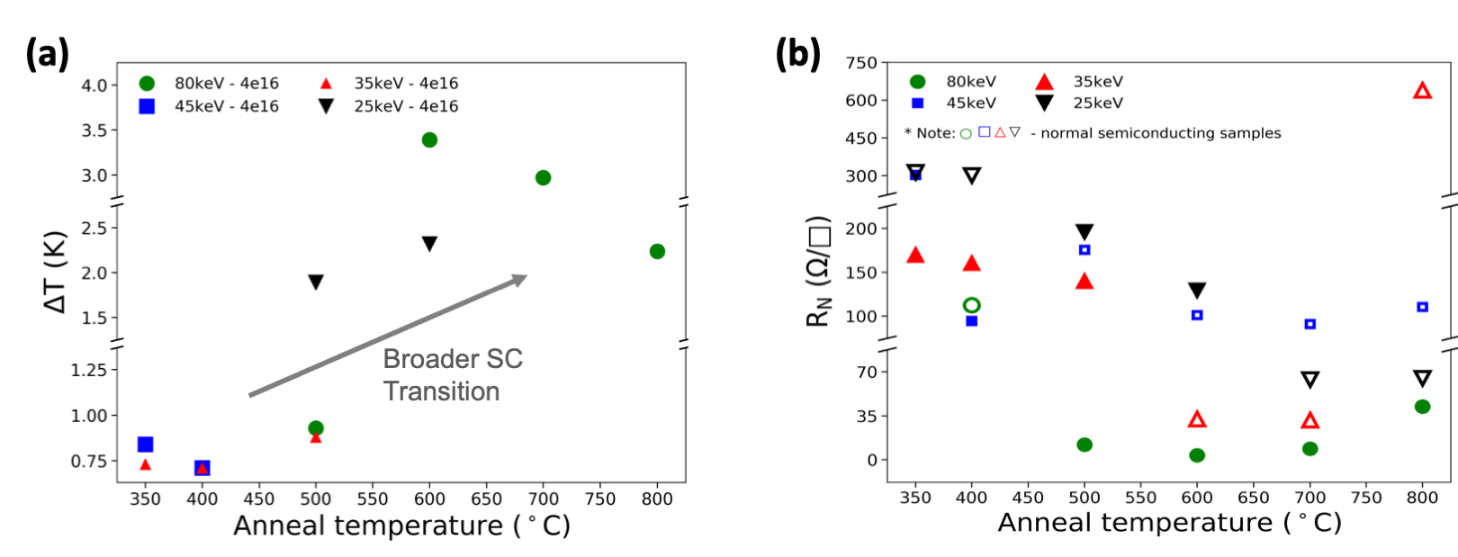
Dependence of superconducting transition temperature () on EIMP and TDA, for the samples with complete transition to zero-resistance phase (i.e. ”SC”), is shown in Figure 1d. The Tc values were extracted from sheet resistance vs. temperature curves at points where resistance is 50% of normal resistance at 10 K. is relatively constant within the margins of error for the sample with EIMP = 80 keV. By reducing EIMP to 45 and 35 keV, where Ga peak is still within the Ge substrate (see Figure 1b), is lowered to minimum value of 2 K while the normal-superconductor transition became sharper (see supplementary figure S2 for an overview transition widths). However, for EIMP = 25 keV, the Tc one again raises to 3.5 and 4.0 K for the two superconducting samples with TDA = 500 ∘C and 600 ∘C. of 4.0 K, is 1 K above the record value reported in the literature for hyper Ga-doped Ge for Rc = 0.5 Rn. Similarly, the transition widths for for samples with EIMP = 25 keV approach the values for EIMP = 80 keV. At such low EIMPs, as the ion beam spreads over a smaller interaction volume and the majority Ga stays inside the barrier, significant mixing between Ge, Ga and SiO2 is expected. Therefore, a higher density of structural defects may be expected in the 25 keV samples, leading to more non-trivial transitional behavior.
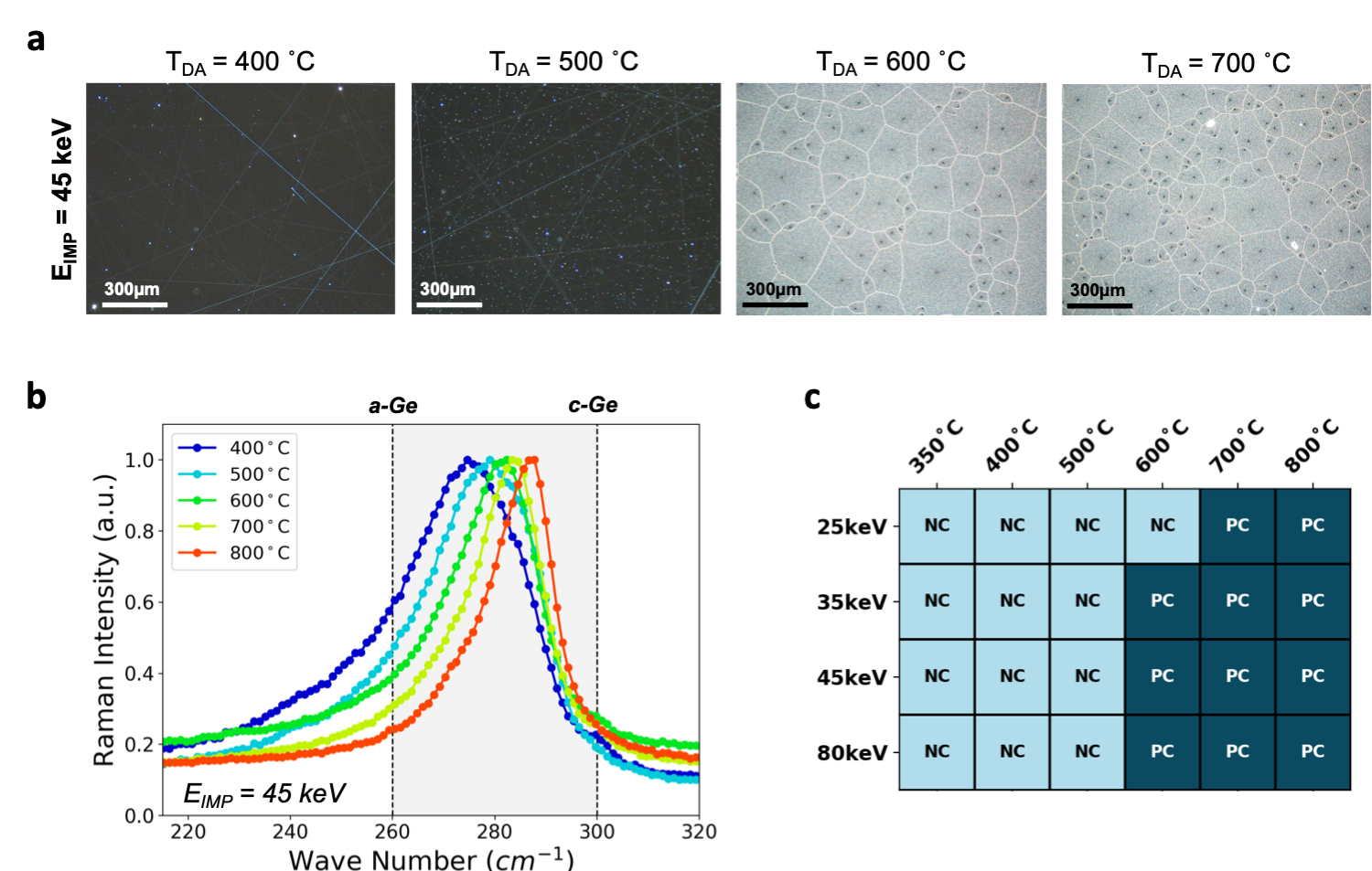
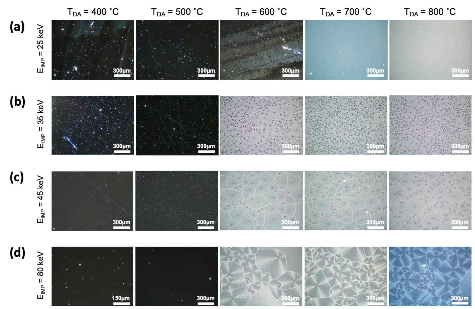
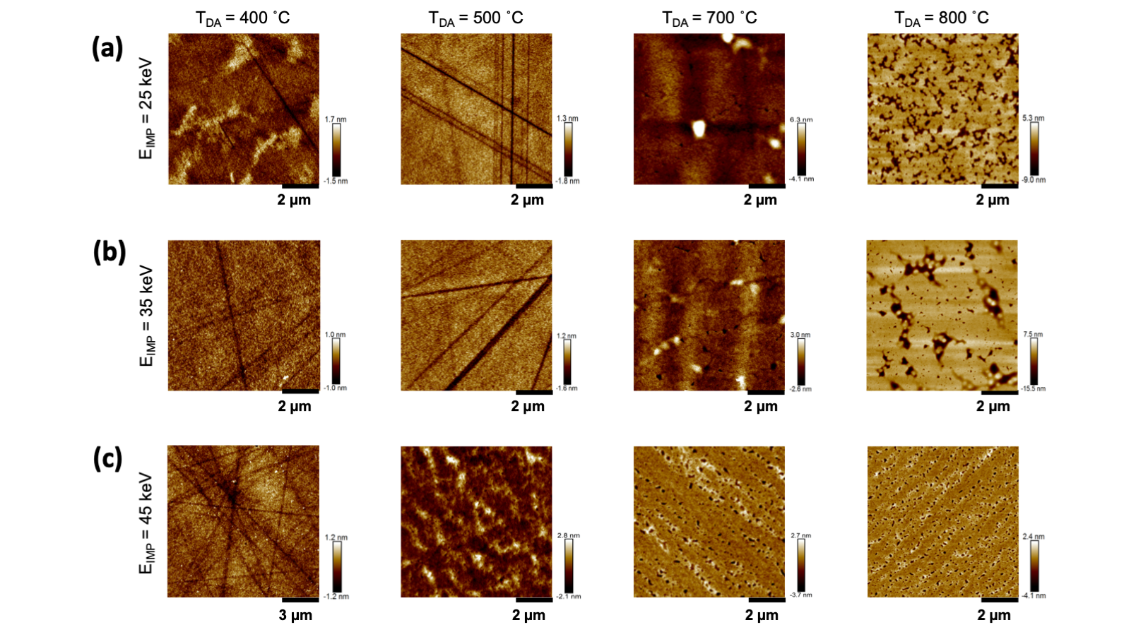
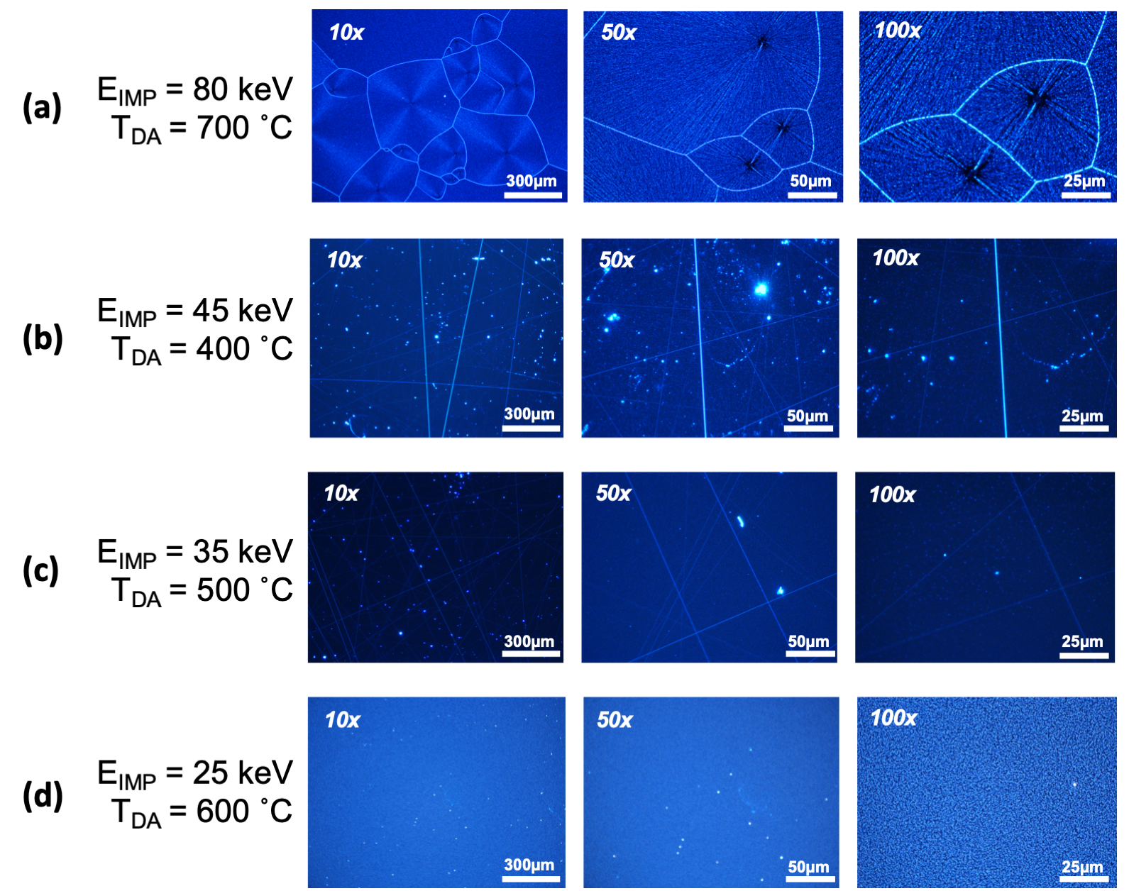
Structural and compositional characterization. Variations in the EIMP and TDA have significant impact on the microstructure of the films. Figure 2a shows the dark field (DF) optical images of the films prepared with EIMP = 45 keV and TDA = 400–700 ∘C. From these DF images it is clear that between 500 ∘C and 600 ∘C, a transition occurs from crossing lines patterns to a poly-crystalline structure with a few hundred wide grains. This behavior has been more or less observed at all implantation energies tested in this study (see figure S3). Nonetheless, the average grain size for the surfaces with EIMP = 25 keV is much smaller than other energies, leading to DF images with no micron-size features. In addition, the crossing lines are only present for E 80 keV. These lines were confirmed to be actual topographical features a few depth as confirmed by atomic force microscopy measurements (see supplementary figures S4 and S5).
The crystallinity of the samples were further investigated by monitoring the Ge Raman peak position as a function of TDA, as illustrated in figure 2b. While implantation process led to near-complete amorphization of the top surface (spectrum not shown here), increasing the annealing temperature coincides with the Ge Raman peak shift from near amorphous Ge (a-Ge) to values closer to crystalline Ge (c-Ge) 40; 41. This trend of increasing crystallinity with TDA was universally seen across all implantation energies (see supplementary figure S5). However, for lower shallower Ga+ implantation (i.e. EIMP = 25 and 35 keV), especially at lower annealing temperature, secondary peak is noticed at 300 cm-1, consistent with signal detected from the c-Ge below the implanted region.
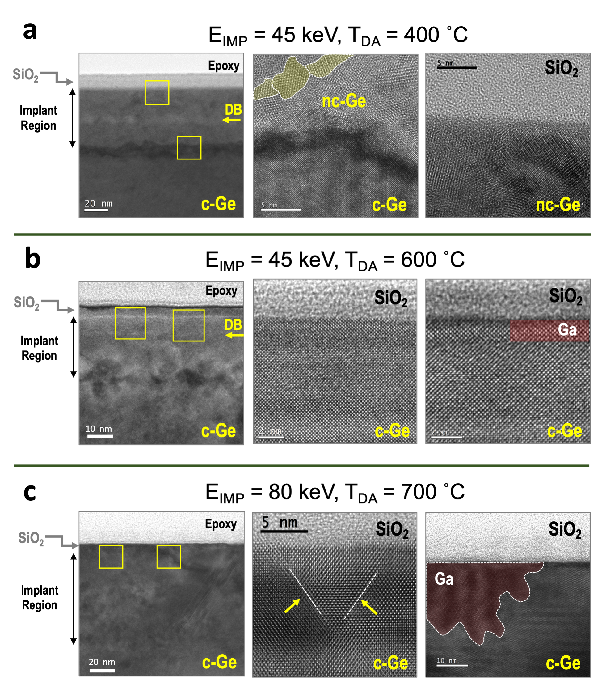
Figure 2c summarizes our findings on the structure of the sample as a function of implantation energy and activation annealing temperature. Based on the DF optical images and Raman peak position, samples were divided into two general groups: i) Nano-crystalline (NC) with dark DF images and Raman shift closer to a-Ge; ii) Poly-crystalline (PC) with clear grain structure visible to optical microscopy and Raman peaks near c-Ge. Comparing this table with figure 1c, we note that for E 80 keV, only nano-crystalline films are superconducting with a zero-resistance state above 1.5 K. PC surfaces at those energies only ”L.SC” with transitions around T = 6 K (near Tc for -Ga 42 and Ga:Si14). Instead, when EIMP = 80 keV, the superconducting behavior spans from NC (TDA = 500 ∘C) to PC (T 600 ∘C). Considering that the NC-PC transition occurs at relatively similar temperatures for all implantation energies, this difference in superconductivity may be attributed to the average depth distribution of Ga within the sample. For shallower Ga peaks, while higher anneal temperature successfully recovers parts of the surface crystallinity, it leads to a larger loss of Ga from the top surface into surface droplets or Ga vapor. For the samples with EIMP=80 keV, the average Ga atoms lie further from the top surface Ga clustering within the implanted region or near the SiO2/Ge may be kinetically more favorable.
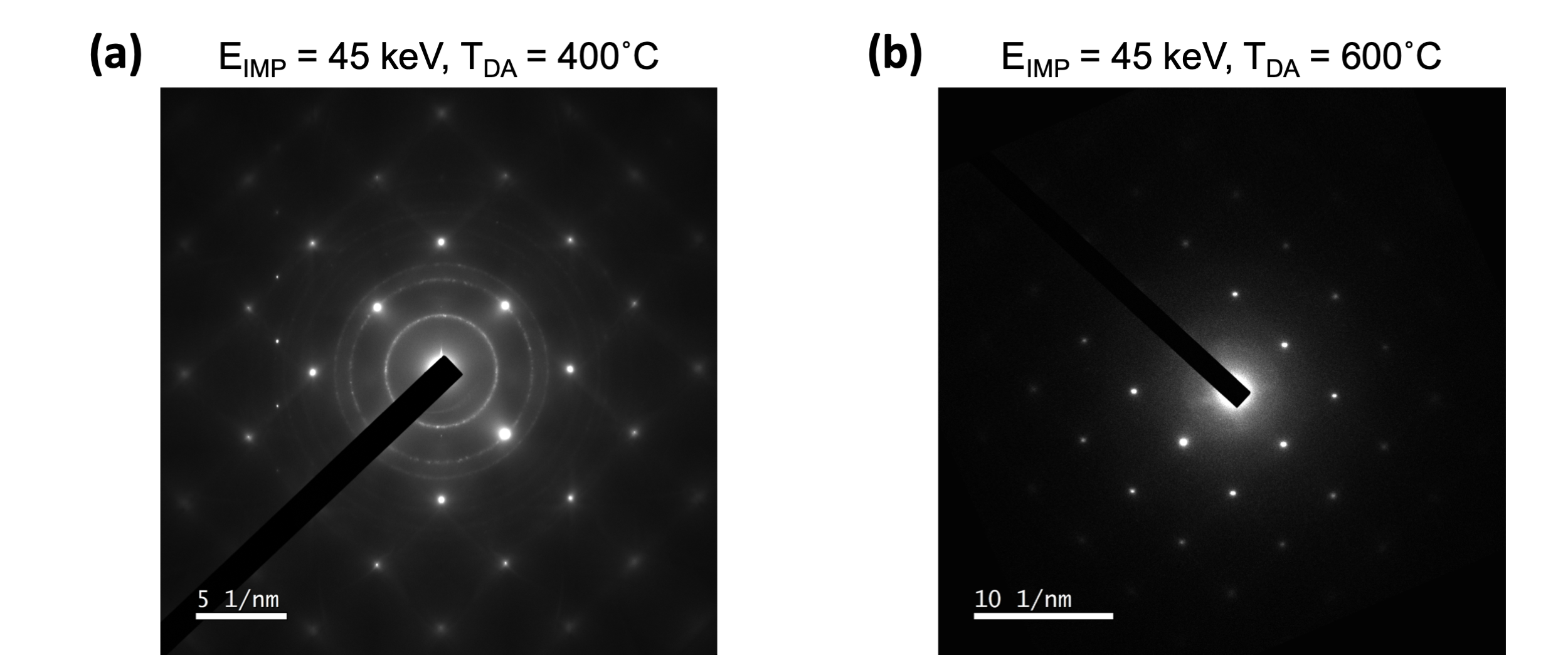
Structures of the implanted samples after dopant activation annealing were examined more closely by Transmission Electron Microscopy (TEM). As shown in Figure 3, a select number of samples with clear NC and PC structures were characterized by TEM. These are representative systems for shallow and deep Ga+ implantation. The samples with EIMP = 45 keV (shown in figure 3a and 3b) have a disturbed band 25 nm below SiO2 barrier due to & recoil during the implantation process. Focusing on the Ge surrounding the disturbed band, annealing at 400 ∘C forms a multi-crystalline film with a few wide grains (NC phase). In contrary, annealing at 600 ∘C helped recover the crystallinity to a significant level, and allowed formation of a few monolayers thick crystalline Ga at the SiO2/Ge interface (highlighted in red, right column in figure 3b). Such crystalline Ga layer appears to be discontinuous as evidenced by its absence in other high-resolution images of theSiO2/Ge interface (middle column in figure 3b). This is consistent with the observation of a 6-K transition (-Ga transition42) to a non-zero resistance state. The difference in the crystallinity of these two systems was confirmed by electron diffraction measurements (see figure S7).
Figure 3c displays the cross-sections of a Ge sample with EIMP = 80 keV and TDA = 700 ∘C. Compared to the samples with EIMP = 45 keV, the depth of the region disturbed by the implanting ions appears to be more than 2x larger. In addition, no visible sign of a disturbed band is present below the SiO2 barrier. Under these conditions, the implanted region appears to consist of highly crystalline Ge in the 15-20 nm lenght scale, although with imperfections such as stacking faults (marked by dotted lines in figure 3c, middle column). Besides, the annealing temperature tended to be high enough to enable formation of large crystalline Ga puddles ( 25 wide) within the implanted region adjacent to the SiO2/Ge interface (right-most column in figure 3c).
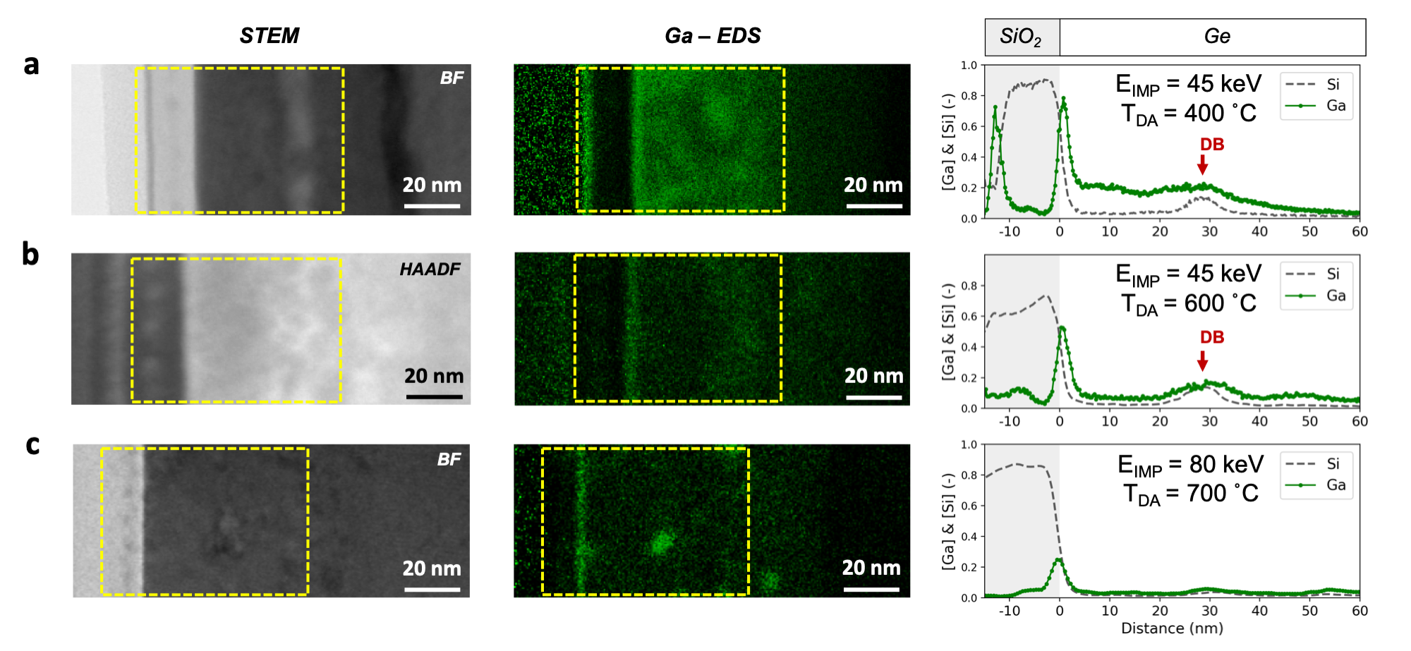
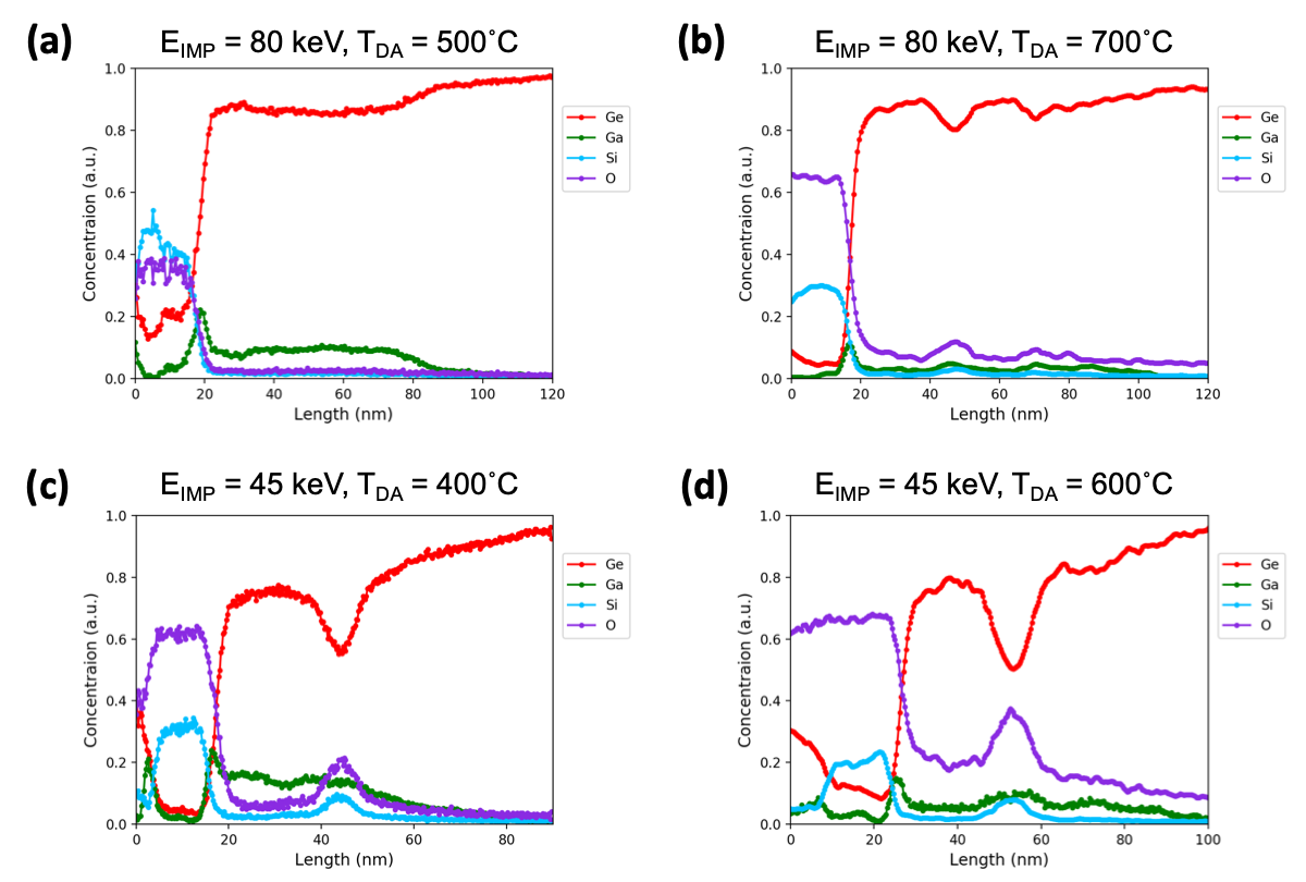
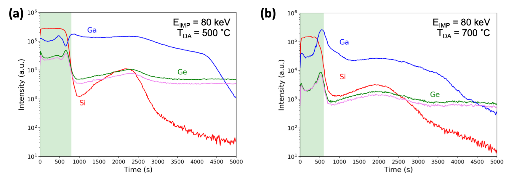
To better determine the Ga distribution in the samples, TEM measurements were complemented by Scanning Transmission Electron Microscopy (STEM) and Energy dispersive Spectroscopy (EDS) compositional mapping. Figure 4 shows the STEM images, Ga elemental maps, and line traces of normalized Si & Ga concentrations (i.e. [Ga] = Ga%/ (Si%+Ge%)) for the three samples discussed above. For samples with EIMP = 45 keV (figure 4a and b), once again disturbed bands were seen at 25-30 below the SiO2 interfaces, with excess amounts Si, O and Ga (see supplementary figure S8 for Ge and O line scans). For the sample with EIMP = 80 keV shown in figure 4c, only small Ga-rich clusters were observed, confirming that disturbed band is only a product of low-energy implantation.
At EIMP = 45 keV & TDA = 400 ∘C, relatively large [Ga] ( 20%) are trapped within the implanted region, particularly in between the SiO2 and the disturbed band (figure 4a). Additionally,sharp Ga peaks were seen both at the SiO2/Ge interface and SiO2 top surfaces. With raising the annealing temperature to 600 ∘C, the Ga atoms seem to diffuse through the structure both towards the Ge substrate and the top barrier (figure 4b). This is evidenced by reduced [Ga] within the implanted region (including interfaces and disturbed band), and enhanced [Ga] below the band. These results are also consistent with the high-resolution TEM images in figure 3b, where there is no abrupt boundary between implanted region and Ge substrate. Elemental mapping for the Ge sample with EIMP = 80 keV & TDA = 700 ∘C (shown in figure 4c) displays small [Ga] ( 5%) within the implanted region, only concentrated in clusters that are dispersed across the cross-section, with spacing in the order of 20 . Moreover, Ga accumulates at the SiO2/Ge interfaces into a thin layer with a peak relative concentration of 25% (more than 2x smaller peaks in samples with EIMP = 45keV). For samples with EIMP = 80keV, the amount of Ga within the bulk of the implanted region and relative height of the interface Ga peak may also be controlled by varying T (see supplementary information figure S8a & b, figure S9).
Another piece of information that may be crucial in explaining the role of Ga distribution in the superconductivity of the PC and NC phases is the amount of Ga incorporated into the Ge lattice as a dopant. Therefore, we measured the hole density (nh) for several samples with various EIMPs. Details of the Hall measurements are provided in supplementary information (figure S11, table LABEL:Table_S1). At EIMP = 45 keV, nh increases from 5.77 x 10¹⁵ to 1.66 x 10¹⁶ , by raising TDA from 400 ∘C to 600 ∘C. However, the increase in TDA also led to the lower [Ga] within the implanted region and loss of superconductivity. The situation is similar for samples with EIMP = 35 keV, where the increase in (nh) results in a normal metallic behavior. These results confirm that Ga does not (at least solely) contribute to superconductivity as a dopant, but as a segregated phase (amorphous or crystalline) present within the bulk or at the SiO2/Ge interfaces.
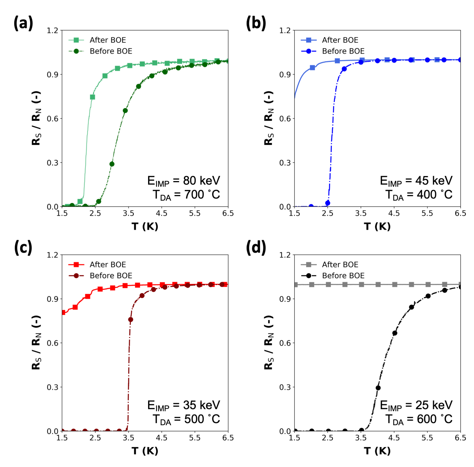
The difference in superconductivity mechanism for PC vs. NC samples was further revealed by 15s of SiO2 etch (using 6:1 buffer oxide etchant(BOE)). Despite no effect on the microstructure (supplementary information figure S11) and minimal reactivity with Ga, the enchant is expected to remove Ga through removal of its host matrix (Ge and SiO2) 43. Rs(T) measurements illustrated that the BOE etch has a pronounced effect on the superconducting phase at all EIMPs. Only the PC sample with EIMP = 80 keV retains its superconductivity after etch, although with lower Tc and Bc (see supplementary information figure S12). This implies that a portion of the superconductivity for this sample resides sub-surface, possibly induced by Josephson coupling between the Ga-rich clusters that are dispersed within the implanted region 38. In contrast, in all NC samples with EIMP 45 keV, the zero-resistance state disappeared after etch. At T 1.5 K, the etch effect becomes more dramatic as EIMP becomes smaller, with a fully metallic behavior for the 25 keV sample. Combining the etch results with the TEM and EDS studies, it may be concluded that the superconductivity with zero resistance for NC samples is only provided by the Ga constricted 3–5nm below the SiO2 barrier.
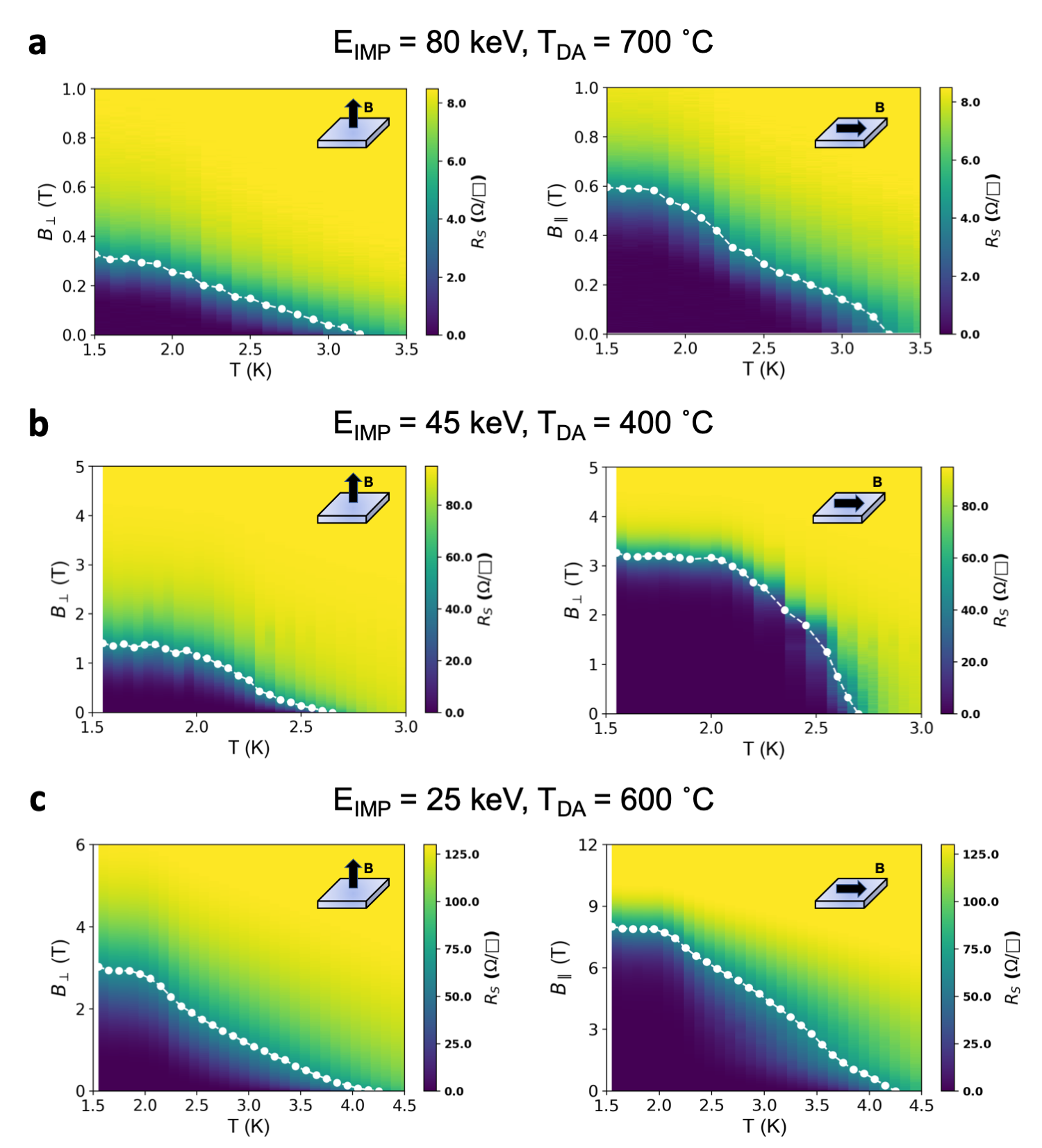
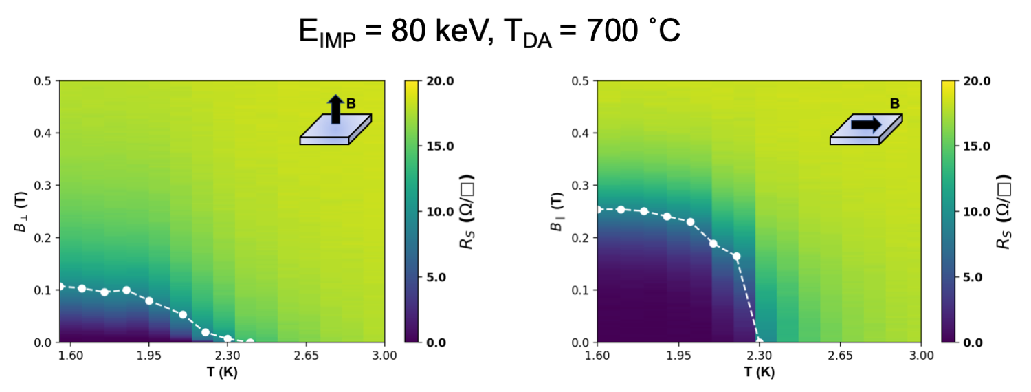
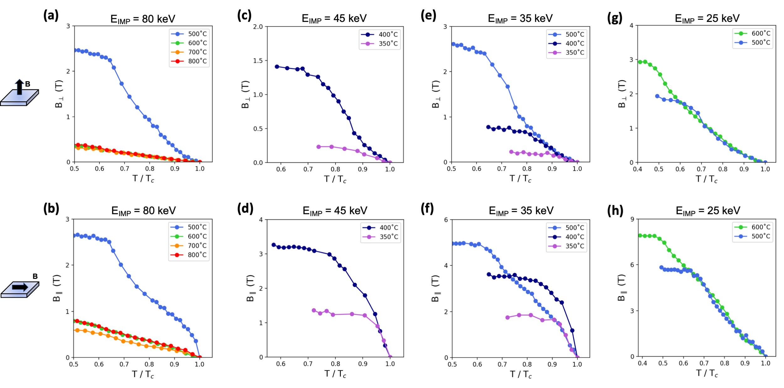
Temperature dependence of Resistive Critical Fields. Next, we turn to study the effect of Ga-doped Ge phase (NC or PC) can have on the superconductor–normal transitions under magnetic fields. For all superconducting samples labeled as ”SC” in figure 1c, temperature dependence of Rs(B) was measured under in-plane (B⟂) and out-of-plane (B∥) magnetic fields as high 12 T. Figure 5 displays Rs(B) vs. temperature heat maps for measured for three samples with EIMP = 80 keV (a), 45 keV (b), and 25 keV (c). The resistive critical field (Bc) at each temperature, is defined as the field at which Rs = 0.5 . The overlay plots in figure 5 indicate temperature dependence of Bc, which is often known as the boundary for the superconducting-metal phase transition 27; 44. A more comprehensive version of Bc phase boundary curves for all ”SC” samples is provided in the supplementary information (figure S14).
| EIMP | TDA | Clogston | Chandrasekhar | |||
|---|---|---|---|---|---|---|
| limit, Ref.45 | limit, Ref.46 | |||||
| (keV) | (C) | (K) | (T) | (T) | (T) | (T) |
| 80 keV | 700 | 3.3 | 0.32 | 0.59 | 5.94 | 8.58 |
| 45 keV | 400 | 2.65 | 1.39 | 3.22 | 4.77 | 6.89 |
| 25 keV | 600 | 4.25 | 2.97 | 7.95 | 7.65 | 11.05 |
Table 1 summarizes the key superconducting parameters extracted from the Bc–T curves in figure 5a–c. While the Bc(T) for many superconductors follows the Bardeen-Cooper-Schrieffer (BCS) parabolic form Bc = B0[1 - (T/Tc)2], the phase boundaries outlined in figure 5 show significant deviations from that behavior. Therefore, instead of reporting zero-temperature critical magnetic field (B0) we limit our discussion to Bc at 1.55 K, near the base temperature of our cryostat. Table 1 also includes the Clogston 45 and Chandrasekhar 46 upper critical field limits, estimated originally for disordered type-II superconductors with filamentary phases. PC phases with exhibit EIMP = 80 keV have Bc values well below these limits in both in-plane and out-of-plane configurations. On the other hand, by going to lower EIMP (e.g. 45 keV & 25 keV), we saw significant increases in the Bc of NC phases, nearing their Clogston limit (see supplementary table LABEL:Table_S2). In the extreme case of EIMP = 25 keV, B∥ even surpassed the limit by 0.3 T. Similar behavior has been reported for thin lead films, where in these studies this is attributed to strong spin-orbit coupling in the 2D metal 47.
The in-plane Bc(T) phase boundary is a macroscopic property that reflects the dimensionality of the superconductive phases involved 48. The phase boundary behavior is particularly effective in evaluating the dimensionality in layered normal-superconductor systems 49; 50. For 3D superconductivity, the in-plane Bc is expected to follow the Ginzburg-Landau (GL) linear relationship equation with Bc 1 - (T/Tc). In turn, for 2D superconductivity, the in-plane Bc(T) should take the form Bc . However, by a closer look at the in-plane Bc(T) in figure 5 and S14, we find that the PC samples exhibit large linear sections that may be connected to a 3D network of coupled Ga superconducting puddles while most NC samples illustrate negative curvatures that could be attributed to a pseudo-2D network that follows Bc , with .
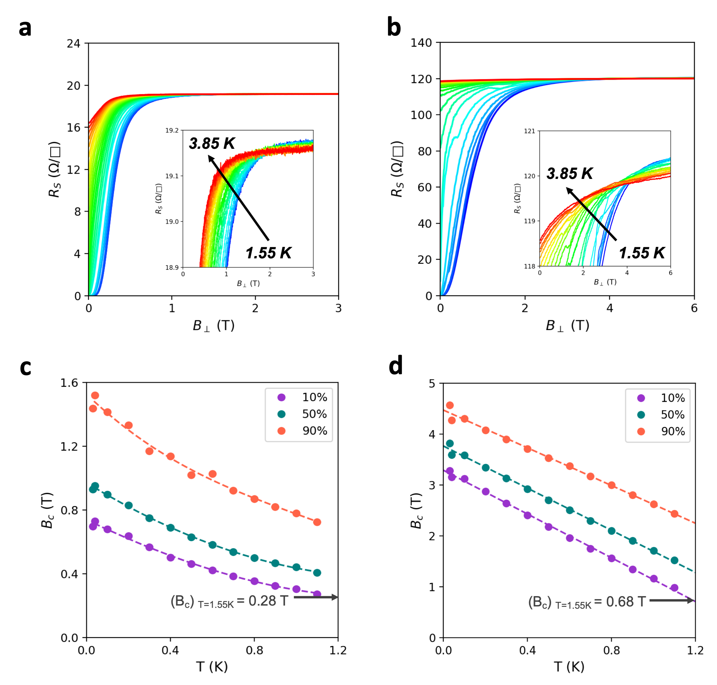
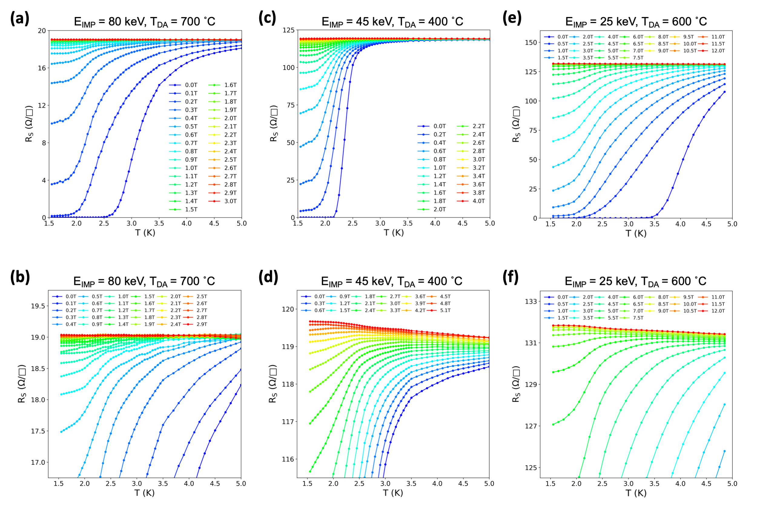
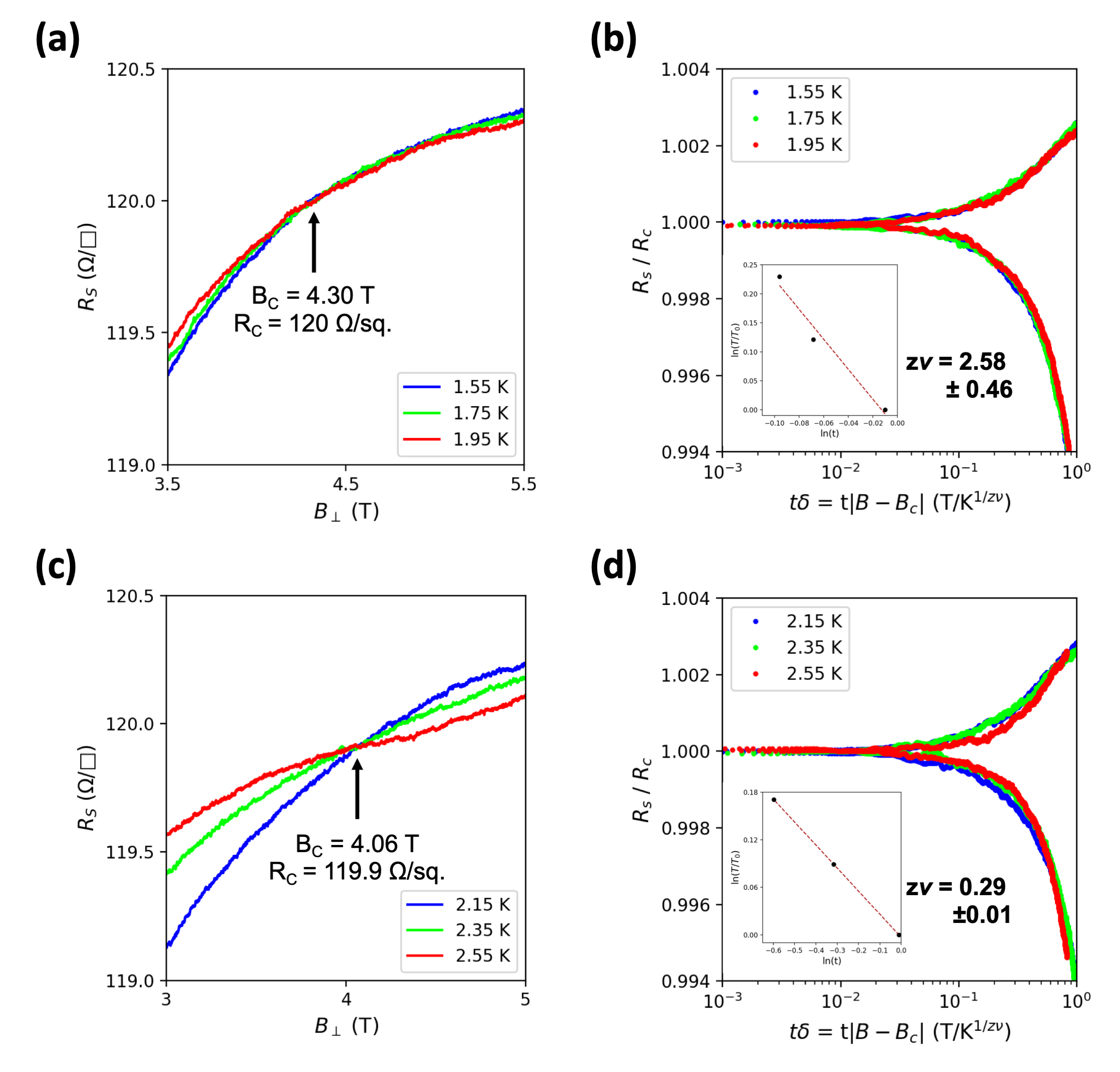
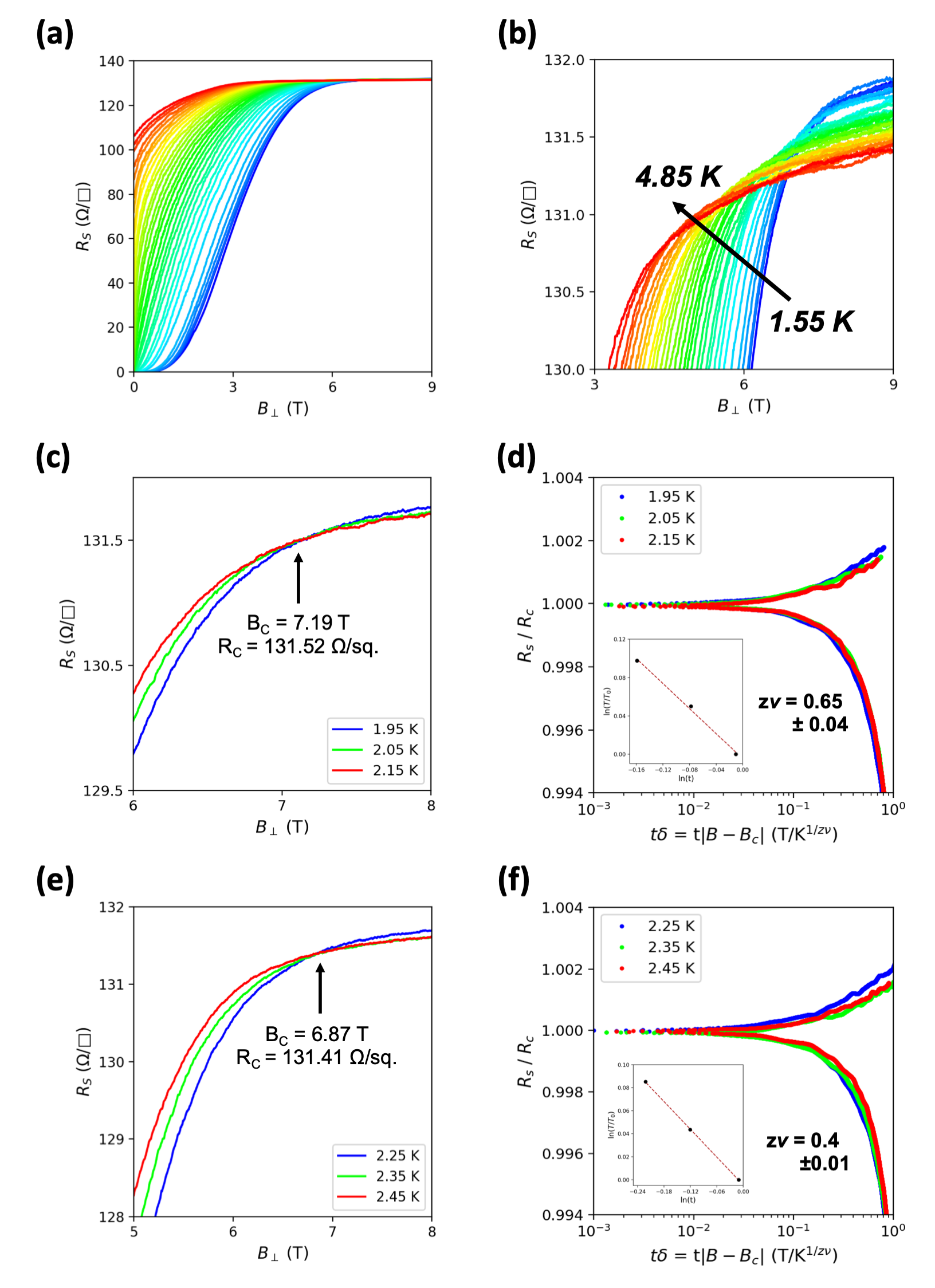
Relatively large Bc with complex temperature dependence are not the only signatures of disordered superconductivity observed in the heavily Ga-doped Ge samples. Figure 6 a & b display the Rs(B) isotherms measured at 1.55–3.85 K for two samples with EIMP = 80keV & TDA = 700 ∘C (a) and EIMP = 45keV & TDA = 400 ∘C (b). In both samples crossing points in Rs(B) were measured at 1.9 T and 4 T, respectively, which are believed to be evidence of quantum phase transition (QPT) in quasi-2D disorder superconductors 29; 51; 52. Rs (T) behavior vs. magnetic field (supplementary figure S15), indicated a more obvious superconductor-metal transition (SMT) from dR/dT0 to dR/dT0 in the sample with EIMP = 45 keV. Because of clear SMT along with better-resolved Rs(B) crossings, we conducted scaling analysis on this sample to explore the possibility of observing Griffiths singularity behavior with divergent product of correlation length exponent () and dynamical critical exponent () 53; 54. Details of scaling analysis are provided in the supplementary materials (see figure S16). For the sample with EIMP = 45 keV, scaling analysis yielded = 2.58 0.46 at T = 1.55–1.95 K range, followed by = 0.29 0.01 at T = 2.15–2.55 K range. Similar analysis on a sample with EIMP = 35 keV led to of 0.65 0.04 at T = 1.55–1.95 K and 0.4 0.01 at T = 2.15–2.55 K (supplemental figure S17). While these values do not establish a trend to a divergent dynamical critical exponent, the general behavior may warrant further investigation into their SMT at near-zero temperatures and high magnetic fields.
Another signature of anomaly was observed in these samples when Bc temperature dependence was measure at near-zero temperatures (i.e. 35 mK–1.1 K). As shown in 6 c & d, both samples with EIMP = 80 keV & TDA = 700 ∘C (c) and EIMP = 45 keV & TDA = 400 ∘C (d), show anomalous rise in as temperature approaches 0 K . This anomaly persists regardless of the definition used for , including at critical sheet resistance = 0.1 , 0.5 and 0.9 . This vs. T upturn is yet another evidence of disorder in these system. The more interesting feature is the difference between the upturn between the two samples; from exponential in figure 6c to linear in figure 6d. The exponential behavior can be explained by a model of superconducting island weakly coupled via Josephson effect, in which the value of the Bc is determined by an interplay between proximity effect and quantum phase fluctuations 55. In turn, the linear Bc(T) anomaly has been recently attributed to vortex glass ground states and their thermal fluctuations present in disordered thin-films 28.
Discussion
In this work, we demonstrated pathways to control the structural and physical characteristics of superconducting phases prepared by hyperdoping of Ge via Ga+ implantation. The parameter space for observing superconductivity in hyperdoped Ge has been clearly expanded to temperatures far below Ge melting point (as low as 350 ∘C) and implantation energies as low as 25 keV. The phase of the superconductor may be tuned by the implantation energy and dopant activation temperatures. Two distinct phases of superconducting materials are recognized: i) 3D poly-crystalline (e.g. at EIMP80 keV, TDA = 700 ∘C ) which is consistent with earlier studies; ii) a new 2D nano-crystalline phase (e.g. at EIMP45 keV, TDA = 400 ∘C ). We find signatures that the nano-crystalline phase superconductivity stems from few thick Ga layer accumulated near the top surface, leading to systems with high quasi-2D disorder as evidenced by various anomalies in critical field behaviors. Both phases showed signatures of strong disorder despite the difference in underlying superconductivity mechanisms. This warrants further investigations into tunability of disorder in these material systems as test-beds for quantum phase transition studies as well as platforms for superconducting circuits with high kinetic inductance.
Methods
Fabrication. Undoped Ge(100) wafers grown by floating zone method with room-temperature resistivity of 40 were used. Prior to implantation, Ge native oxide was etched cyclic immersion in 10% HF solution and DI–H2O. This was followed by the deposition of 30 thick SiO2 top barriers via plasma-enhanced chemical vapor deposition (PECVD). The oxide barrier helps minimize direct damage to the Ge substrates during the ion implantation process. Ga+ ion implantation processes (by Kroko Inc.) were carried out at 25 keV, 35 keV, 45 keV, and 80 keV with a fixed ion fluence of 4e16 cm-2. Throughout the implantation substrates were held at room temperature. After implantation dopants were activated using rapid thermal annealing (RTA) under 5 standard liter per minute (SLPM) of N2 flow and at 350 ∘C to 800 ∘C, for 1 min.
Transport Measurements. Electrical properties of the samples were evaluated by measuring the differential resistance (i.e. ), using lock-in amplifiers, for 5 x 5 square samples in Van der Pauw (VdP) geometry. The AC excitation current for the measurements varied between 1 and 20 A. Measurements down to 1.5 K were performed in a Teslatron PT (Oxford Instruments) cryogen-free refrigerator with maximum magnetic field of 12 T (along z-axis). Measurements below 1.2 K were carried out in a Triton dilution refrigerator (Oxford Instruments) with a 3-axis vector magnet, and maximum z field of 6T. Hall measurements were performed on L-shaped bars. Hall bars were fabricated by UV photolithography followed by reactive ion etching of the mesa using CF4/O2 gas mixtures for 2-5 min. The resulting mesa heights varied between 500 and 1.2 (further details in supplementary information).
Structural and Chemical Characterization. Micro-Raman spectroscopy was performed using a Horiba Xplora -Raman system with a 532 laser and an objective lens at 1000x magnification. Time-of-Flight Secondary ion mass spectrometer (ToF-SIMS) measurements were performed using Bi+ and Ga+ ions for detection and Ar+ ions for milling. Ion detection was done in positive ion mode by monitoring 28Si, 72Ge, 74Ge, 69Ga and 12C. Atomic force microscopy (AFM) was performed in order to determine the surface morphology of the superconducting films in details. A Bruker Dimension Fastscan scanning probe microscopy system was used in tapping mode (ScanAsyst mode). The AFM probes used for the measurements were Bruker FASTSCAN-B, made of silicon nitride with triangular tips of 5–12 radius.
Electron Microscopy. The crystal morphology of the structures were examined with with transmission electron microscopy (TEM) in a JEOL ARM200F equipped, with a spherical aberration corrector for probe mode, operated at 200 keV. The composition of each films was studied with energy dispersive spectroscopy (EDS). The samples were prepared with cross-sectional tripod polishing to 20 thickness, followed by shallow angle Ar+ ion milling with low beam energies ( 3 keV), and LN2 stage cooling in a PIPS II ion mill.
References
- 1 Shabani, J. et al. Two-dimensional epitaxial superconductor-semiconductor heterostructures: A platform for topological superconducting networks. Phys. Rev. B 93, 155402 (2016).
- 2 Krogstrup, P. et al. Epitaxy of semiconductor–superconductor nanowires. Nature Materials 14, 400–406 (2015).
- 3 Mayer, W. et al. Superconducting proximity effect in epitaxial Al-InAs heterostructures. Appl. Phys. Lett. 114, 103104 (2019).
- 4 Casparis, L. et al. Superconducting gatemon qubit based on a proximitized two-dimensional electron gas. Nature Nanotech 13, 915–919 (2018).
- 5 Casparis, L. et al. Voltage-controlled superconducting quantum bus. Phys. Rev. B 99, 085434 (2019).
- 6 Mayer, W. et al. Gate controlled anomalous phase shift in Al/InAs Josephson junctions. Nature Communications 11, 212 (2020).
- 7 Fornieri, A. Evidence of topological superconductivity in planar josephson junctions. Nature 569 (2019).
- 8 Mayer, W. et al. Phase signature of topological transition in josephson junctions. arXiv (2019). eprint 1906.01179.
- 9 Shim, Y.-P. & Tahan, C. Bottom-up superconducting and Josephson junction devices inside a group-IV semiconductor. Nat Commun 5, 4225 (2014).
- 10 Shim, Y.-P. & Tahan, C. Superconducting-Semiconductor Quantum Devices: From Qubits to Particle Detectors. IEEE Journal of Selected Topics in Quantum Electronics 21, 1–9 (2015).
- 11 Ekimov, E. A. et al. Superconductivity in diamond. Nature 428, 4 (2004).
- 12 Okazaki, H. et al. Signature of high T above 25 K in high quality superconducting diamond. Appl. Phys. Lett. 106, 052601 (2015).
- 13 Bustarret, E. et al. Superconductivity in doped cubic silicon. Nature 444, 465–468 (2006).
- 14 Skrotzki, R. et al. On-chip superconductivity via gallium overdoping of silicon. Appl. Phys. Lett. 97, 192505 (2010).
- 15 Thorgrimsson, B., McJunkin, T., MacQuarrie, E. R., Coppersmith, S. N. & Eriksson, M. A. The effect of external electric fields on silicon with superconducting gallium nano-precipitates. Journal of Applied Physics 127, 215102 (2020). URL https://aip.scitation.org/doi/10.1063/5.0002460. Publisher: American Institute of Physics.
- 16 Herrmannsdörfer, T. et al. Superconducting State in a Gallium-Doped Germanium Layer at Low Temperatures. Phys. Rev. Lett. 102, 217003 (2009).
- 17 Fiedler, J. et al. Superconducting Ga-overdoped Ge layers capped with SiO 2 : Structural and transport investigations. Phys. Rev. B 85, 134530 (2012).
- 18 Cohen, M. L. Superconductivity in Many-Valley Semiconductors and in Semimetals. Phys. Rev. 134, A511–A521 (1964).
- 19 Blase, X., Bustarret, E., Chapelier, C., Klein, T. & Marcenat, C. Superconducting group-IV semiconductors. Nature Mater 8, 375–382 (2009).
- 20 Scappucci, G. et al. The germanium quantum information route. arXiv:2004.08133 (2020).
- 21 Fiedler, J. et al. Superconducting films fabricated by high-fluence Ga implantation in Si. Phys. Rev. B 83, 214504 (2011).
- 22 Skrotzki, R. et al. The impact of heavy Ga doping on superconductivity in germanium. Low Temperature Physics 37, 877–883 (2011).
- 23 Prucnal, S. et al. Superconductivity in single-crystalline aluminum- and gallium-hyperdoped germanium. Phys. Rev. Materials 3, 054802 (2019).
- 24 Olesinski, R. W. & Abbaschian, G. J. The Ga−Ge (Gallium-Germanium) system. Bulletin of Alloy Phase Diagrams 6, 258–262 (1985).
- 25 Herrmannsdörfer, T. et al. Superconductivity in thin-film germanium in the temperature regime around 1 K. Supercond. Sci. Technol. 23, 034007 (2010).
- 26 Gregory, W. D., Sheahen, T. P. & Cochran, J. F. Superconducting Transition and Critical Field of Pure Gallium Single Crystals. Phys. Rev. 150, 315–321 (1966).
- 27 Spivak, B., Oreto, P. & Kivelson, S. A. Theory of quantum metal to superconductor transitions in highly conducting systems. Phys. Rev. B 77, 214523 (2008).
- 28 Sacépé, B. et al. Low-temperature anomaly in disordered superconductors near Bc2 as a vortex-glass property. Nature Phys 15, 48–53 (2019).
- 29 Xing, Y. et al. Quantum Griffiths singularity of superconductor-metal transition in Ga thin films. Science 350, 542–545 (2015).
- 30 Saito, Y., Nojima, T. & Iwasa, Y. Quantum phase transitions in highly crystalline two-dimensional superconductors. Nature Communications 9, 778 (2018).
- 31 Hazard, T. et al. Nanowire Superinductance Fluxonium Qubit. Phys. Rev. Lett. 122, 010504 (2019).
- 32 Niepce, D., Burnett, J. & Bylander, J. High Kinetic Inductance $\mathrm{Nb}\mathrm{N}$ Nanowire Superinductors. Phys. Rev. Applied 11, 044014 (2019).
- 33 Samkharadze, N. et al. High-Kinetic-Inductance Superconducting Nanowire Resonators for Circuit QED in a Magnetic Field. Phys. Rev. Applied 5, 044004 (2016).
- 34 Peltonen, J. T. et al. Hybrid rf SQUID qubit based on high kinetic inductance. Scientific Reports 8, 10033 (2018).
- 35 Astafiev, O. V. et al. Coherent quantum phase slip. Nature 484, 355–358 (2012).
- 36 Ziegler, J. F. The Stopping and Ranges of Ions in Matter: Handbook of Stopping Cross-Sections for Energetic Ions in All Elements (Elsevier, 2013).
- 37 Heera, V. et al. Depth-resolved transport measurements and atom-probe tomography of heterogeneous, superconducting Ge:Ga films. Supercond. Sci. Technol. 27, 055025 (2014).
- 38 Deutscher, G., Grave, I. & Alexander, S. Upper Critical Field of a Percolating Superconductor. Phys. Rev. Lett. 48, 1497–1500 (1982).
- 39 John, S. & Lubensky, T. C. Phase transitions in a disordered granular superconductor near percolation. Phys. Rev. B 34, 4815–4825 (1986).
- 40 Johnson, B. C., Deam, L., Lee, K. K., Rubanov, S. & McCallum, J. C. Solid phase epitaxial regrowth of germanium containing nanoporous structures formed by ion implantation. AIP Conference Proceedings 1583, 230–234 (2014).
- 41 Olivares, J. et al. Raman spectroscopy study of amorphous SiGe films deposited by low pressure chemical vapor deposition and polycrystalline SiGe films obtained by solid-phase crystallization. Thin Solid Films 358, 56–61 (2000).
- 42 Campanini, D., Diao, Z. & Rydh, A. Raising the superconducting of gallium: In situ characterization of the transformation of -Ga into -Ga. Phys. Rev. B 97, 184517 (2018).
- 43 Johnson, W. C., Parson, J. B. & Crew, M. C. Nitrogen Compounds of Gallium. III. J. Phys. Chem. 36, 2651–2654 (1932).
- 44 Fisher, M. P. A. Dissipation and quantum fluctuations in granular superconductivity. Phys. Rev. B 36, 1917–1930 (1987).
- 45 Clogston, A. M. Upper Limit for the Critical Field in Hard Superconductors. Phys. Rev. Lett. 9, 266–267 (1962).
- 46 Chandrasekhar, B. S. A note on the maximum critical field of high‐field superconductors. Appl. Phys. Lett. 1, 7–8 (1962).
- 47 Nam, H. et al. Ultrathin two-dimensional superconductivity with strong spin–orbit coupling. Proc Natl Acad Sci U S A 113, 10513–10517 (2016).
- 48 Matijasevic, V. Films and Multilayers: Conventional Superconducting. In Buschow, K. H. J. et al. (eds.) Encyclopedia of Materials: Science and Technology, 3181–3187 (Elsevier, Oxford, 2001).
- 49 Krasnov, V. M., Kovalev, A. E., Oboznov, V. A. & Pedersen, N. F. Magnetic field decoupling and 3D-2D crossover in Nb/Cu multilayers. Phys. Rev. B 54, 15448–15456 (1996).
- 50 Obi, Y., Ikebe, M., Fujishiro, H., Takanaka, K. & Fujimori, H. Synthetic Analyses of Tc and Hc2 of NbTi/Nb Superconductor/Superconductor Superlattice. physica status solidi (b) 223, 799–809 (2001).
- 51 Liu, Y. et al. Anomalous quantum Griffiths singularity in ultrathin crystalline lead films. Nature Communications 10, 3633 (2019).
- 52 Zhang, C. et al. Quantum Griffiths singularities in TiO superconducting thin films with insulating normal states. NPG Asia Materials 11, 1–9 (2019).
- 53 Marković, N., Christiansen, C. & Goldman, A. M. Thickness–Magnetic Field Phase Diagram at the Superconductor-Insulator Transition in 2D. Phys. Rev. Lett. 81, 5217–5220 (1998).
- 54 Fisher, M. P. A., Weichman, P. B., Grinstein, G. & Fisher, D. S. Boson localization and the superfluid-insulator transition. Phys. Rev. B 40, 546–570 (1989).
- 55 Galitski, V. M. & Larkin, A. I. Disorder and Quantum Fluctuations in Superconducting Films in Strong Magnetic Fields. Phys. Rev. Lett. 87, 087001 (2001).
Data Availability.
The data that support the findings of this study are available within the paper and its supplementary Information. Additional data are available from the corresponding author upon request.
Acknowledgements
The authors thank Emanuel Tutuc and Fatemeh Barati for fruitful discussions. NYU team is supported by AFOSR Grant No. FA9550-16-1-0348 and ARO Grant No. W911NF1810115 . K.S. thanks Davood Shahjerdi and Edoardo Cuniberto for their assistance with the Raman spectroscopy measurements. K.S. and T.N. thank Tai-De Li of CUNY ASRC surface science suite is acknowledged for his assistance with ToF-SIMS measurements. J.Y. acknowledges funding from the ARO/LPS QuaCGR fellowship reference W911NF1810067.
Authors contributions.
K.S. and T.D.N. synthesized the superconducting film structures and fabricated micro-devices. K.S., T.N., W.L.S., A.L.F, M.H., J.Y. and W.M. performed the measurements with J.S. providing input. K.S., T.N. and M.C.D. performed data analysis. K.S. and J.S. conceived the experiments. All authors contributed to interpreting the data. The manuscript was written by K.S., W.L.S, M.C.D., J.Y. and J.S. with suggestions from all other authors.
I Supplementary information


Hall Measurements
In order to determine the hole concentration in hyper Ga-doped Ge samples, Hall measurements were performed on L-shaped Hall bars as shown in figure S13a. The 150 m wide Hall bars had two contacts, one at each end, for current injection, as well as four pairs of contacts for Hall voltage measurements in two orthonormal directions. Measurements were carried out by sweeping the fields (B) from -6 T to 6 T, perpendicular to the sample surface, while measuring Hall coefficients (RH) in two directions as show in figure S13b. Typically, RH vs. B were recorded from 3 K to 200 K. However, the linear behavior corresponding to hole carriers was only observed below 30 K. This is due to the fact that the Ge substrates have an equilibrium Sb concentration of 1e14 cm-2, making them lightly n-type. The p-n junction that forms between between the Ga-doped region and the substrate is only fully depleted at temperatures below 30 K. Figure S13c displays the RH(B) behavior for a Ge sample with EIMP = 45keV & TDA = 400 ∘C. The negative slope confirms the presence of holes as majority carriers in the sample. All eight samples that were subjects of the Hall measurements showed a negative slope. From the magnitude of the slope () we determined the hole density () in cm-2 using the following equation:
| (S1) |
where is the elementary charge of holes (1.602e-19 C). Since no significant shift was observed in the RH(B) slope vs. temperature, only one value is reported as for each sample. Table LABEL:Table_S1 summarizes the processing conditions and for all 80 samples. In addition to the measured hole density, Ga density in Ge –estimated by SRIM Monte Carlo simulation– is included in the last column.

Estimated hole density by TRIM simulations.
Sample is not superconducting.
| EIMP | TDA | a | ||
|---|---|---|---|---|
| (keV) | (C) | (K) | () | () |
| 80 keV | 800 | 3.4 | 1.07 x 10¹⁶ | 3.46 x 10¹⁶ |
| 80 keV | 500 | 3.0 | 5.48 x 10¹⁵ | |
| 45 keV | 600 | N/Ab | 1.66 x 10¹⁶ | 1.90 x 10¹⁶ |
| 45 keV | 400 | 2.6 | 5.77 x 10¹⁵ | |
| 35 keV | 600 | N/Ab | 1.42 x 10¹⁶ | 1.04 x 10¹⁶ |
| 35 keV | 400 | 2.6 | 5.70 x 10¹⁵ | |
| 25 keV | 700 | N/Ab | 1.90 x 10¹⁵ | 2.38 x 10¹⁵ |
| 25 keV | 500 | 3.3 | 3.41 x 10¹⁵ | |
| \insertTableNotes |
Averaged over the temperature range of 1.5–1.6K.
Clogston limit is B 1.8 Tc.
Chandrasekhar limit is B 2.6 Tc.
| EIMP | TDA | a | a | Clogstonb | Chandrasekhar c | |
|---|---|---|---|---|---|---|
| (keV) | (C) | (K) | (T) | (T) | (T) | (T) |
| 80 keV | 800 | 3.50 | 0.40 | 0.81 | 6.30 | 9.10 |
| 80 keV | 700 | 3.3 | 0.32 | 0.59 | 5.94 | 8.58 |
| 80 keV | 600 | 3.60 | 0.37 | 0.81 | 6.48 | 9.36 |
| 80 keV | 500 | 3.20 | 2.48 | 2.65 | 5.76 | 8.32 |
| 45 keV | 400 | 2.65 | 1.39 | 3.22 | 4.77 | 6.89 |
| 45 keV | 350 | 2.10 | 0.22 | 1.33 | 3.78 | 5.46 |
| 35 keV | 500 | 3.25 | 2.62 | 4.99 | 5.94 | 8.45 |
| 35 keV | 400 | 2.40 | 0.76 | 3.55 | 4.32 | 6.24 |
| 35 keV | 350 | 2.10 | 0.21 | 1.82 | 3.78 | 5.46 |
| 25 keV | 600 | 4.25 | 2.97 | 7.95 | 7.65 | 11.05 |
| 25 keV | 500 | 3.15 | 1.86 | 5.74 | 5.67 | 8.19 |
| \insertTableNotes |
Finite-size Scaling
Finite-size scaling (FSS) analysis was performed to determine the critical exponent product () for the two samples with prominent magnetoresistance crossing features with EIMP = 45keV & TDA = 400 ∘C (figure S16) and EIMP = 25keV & TDA = 600 ∘C (figure S17). The sheet resistance (Rs) for these systems in the zero-temperature quantum critical regime is expected to follow the scaling law of
| (S2) |
where = B - Bc is the offset relative to the critical magnetic field (Bc), and Rc is the critical sheet resistance. These values are critical parameters for the quantum phase transition (QPT). Therefore, they should not be confused with superconductor-insulator transition critical parameters discussed earlier in the paper. Moreover, is an arbitrary scaling function that satisfies , is the coherence length exponent, and is the dynamical critical exponent 53; 54. We determined the effective exponent products for two crossing regions (i.e. 1.55–1.75K, 2.15–2.55K) in the Rs(B) isotherms. Each temperature region, which included three crossing curves, was assigned a critical point with characteristic Bc and Rc. We then defined rewrote equation S2 as Rs() = Rc, where and is the lowest temperature in the critical region (i.e. 1.55K & 2.15K). The parameter, is then found by numerically collapsing other Rs(B) curves onto the curve of lowest temperature. We finally determine the exponent the vs. in each region to a power law in temperature. This is show in insets for figure S16b & d and figure S17d & f.
References
- 1 Marković, N. and Christiansen, C. and Goldman, A. M., Thickness–Magnetic Field Phase Diagram at the Superconductor-Insulator Transition in 2D. Phys. Rev. Lett. 81, 5217–5220 (1998).
- 2 Fisher, Matthew P. A. and Weichman, Peter B. and Grinstein, G. and Fisher, Daniel S. Boson localization and the superfluid-insulator transition. Phys. Rev. B 40, 546–570 (1989).