Biaxial strain enhanced piezoelectric properties in monolayer g-
Abstract
Graphite-like carbon nitride (g-) is considered as a promising candidate for energy materials. In this work, the biaxial strain (-4%-4%) effects on piezoelectric properties of g- monolayer are studied by density functional theory (DFT). It is found that the increasing strain can reduce the elastic coefficient -, and increases piezoelectric stress coefficient , which lead to the enhanced piezoelectric strain coefficient . Compared to unstrained one, strain of 4% can raise the by about 330%. From -4% to 4%, strain can induce the improved ionic contribution to of g-, and almost unchanged electronic contribution, which is different from monolayer (the enhanced electronic contribution and reduced ionic contribution). To prohibit current leakage, a piezoelectric material should be a semiconductor, and g- monolayer is always a semiconductor in considered strain range. Calculated results show that the gap increases from compressive strain to tensile one. At 4% strain, the first and second valence bands cross, which has important effect on transition dipole moment (TDM). Our works provide a strategy to achieve enhanced piezoelectric effect of g- monolayer, which gives a useful guidence for developing efficient energy conversion devices.
pacs:
71.20.-b, 77.65.-j, 72.15.Jf, 78.67.-n Email:sandongyuwang@163.comI Introduction
Analogous to graphene, monolayer g- has been achieved by top-down methods, which provides several potential applications including superior photocatalytic activitiesc2 ; c2-1 , sensingc3 and memory devicesc4 . For example, g- can generate hydrogen from water under visible light with an appropriate band gap of 2.7 eVc5 . Many g-/semiconductor heterostructures have been constructed to improve the photocatalytic performance of g- to restrain the recombination of photogenerated carriers, like g-/c6 , g-/c7 and g-/CdSc8 . Because of non-centrosymmetric structure, the monolayer g- can exhibit a piezoelectricity, which may produce potential piezocatalysis applications.
In fact, due to potential nanoscale piezoelectric applications, the piezoelectricities of two-dimensional (2D) materials have attracted growing interestq4 . Experimentally, the piezoelectric coefficient (=2.9 C/m) of the monolayer has been measured with the 2H phaseq5 ; q6 , and an intrinsic vertical piezoelectric responseq8 has been proved to exist in the Janus MoSSe monolayer. The theoretical studies on piezoelectric properties of 2D materials, such as transition metal dichalchogenides (TMD), Janus TMD, group IIA and IIB metal oxides, group-V binary semiconductors and group III-V semiconductors, have been widely stuided q7 ; q7-1 ; q7-2 ; q7-3 ; q7-4 ; q9 ; q10 ; q11 ; q12 ; qr . The giant piezoelectricities in monolayer SnSe, SnS, GeSe and GeS have been reported, as high as 75-251 pm/Vq10 . A only in-plane piezoelectricity exits in many 2D materials, for example TMD monolayersq9 , and an additional out-of-plane piezoelectricity has also been predicted in many 2D Janus materialsq7 ; q7-2 ; q7-3 . A pure out-of-plane piezoelectric response has been predicted in penta-grapheneq7-4 , and two strategies are proposed to enhance its piezoelectric properties by strain and constructing Janus monolayer. The strain effects on the piezoelectric response of r1 , AsPq7-1 , SnSeq7-1 and Janus TMD monolayersr3 have been reported, and their piezoelectric properties can be effectively tuned. For example, the of SnSe monolayer at -3.5% strain along the armchair direction is up to 628.8 pm/V from unstrained 175.3 pm/Vq7-1 .
In this work, the biaxial strain-tuned piezoelectric properties of g- monolayer are studied by using density functional perturbation theory (DFPT)pv6 . Only in-plane piezoelectricity exists for g- monolayer. The independent piezoelectric constants is predicted to be 1.42 pm/V. It is found that tensile strain of 4% can improve to 6.12 pm/V, which is due to reduced - and enhanced . Different from , increasing strain can enhance the ionic contribution to . It is found that the gap of g- increases from -4% to 4% strain. Strain can also induce the cross between the first and second valence bands, producing important effects on TDM. Therefore, our works give an experimental proposal to achieve enhanced piezoelectricity in g- monolayer.
The rest of the paper is organized as follows. In the next section, we shall give our computational details and methods about piezoelectric coefficients. In the third section, we perform symmetry analysis for elastic and piezoelectric coefficients. In the fourth sections, we shall present main results of g- monolayer. Finally, we shall give our conclusions in the fifth section.
| 7.134 (7.135m1 )[7.130c5 ] | 184.92 | 48.02 | 68.45 |
| 172.45 | 0.26 | 2.77(2.76m1 )[2.7c5 ] | 1.94 (2.18nc ) |
| 3.02 | -1.08 | 1.42 |
II Computational detail
Within the framework of DFT1 , we carry out our calculations by using the VASP codepv1 ; pv2 ; pv3 with the projected augmented wave (PAW) method. A kinetic cutoff energy of 500 eV is adopted, and we use the popular GGA of Perdew, Burke and Ernzerhof (GGA-PBE)pbe as the exchange-correlation potential to calculate piezoelectric and elastic properties. To avoid interactions between two neighboring images, a vacuum spacing of more than 19 along the z direction is added. The total energy convergence criterion is set to eV, and the Hellmann-Feynman forces on each atom are less than 0.0001 . The elastic stiffness tensor and the piezoelectric stress coefficients are calculated by using strain-stress relationship (SSR) and DFPT methodpv6 . Within SSR and DFPT, the electronic and ionic contribution to the elastic and piezoelectric stress coefficients can be calculated directly from VASP code. The Brillouin zone sampling of g- monolayer is done using a Monkhorst-Pack mesh of 11111 for , and 6111 for . The Heyd-Scuseria-Ernzerhof (HSE06) hybrid functional with default parameters is used to obtain the correct electronic structures of monolayer g-. The TDM are calculated by using VASPKIT codevk . The 2D elastic coefficients and piezoelectric stress coefficients have been renormalized by the the length of unit cell along z direction (): = and =.
III Symmetry Analysis
In noncentrosymmetric crystals, a change of polarization can be induced by strain or stress. The phenomenon can be described by the third-rank piezoelectric stress tensors and strain tensor , which are from the sum of ionic and electronic contributions:
| (1) |
and
| (2) |
In which , and are polarization vector, strain and stress, respectively. For 2D materials, if we only consider in-plane strain componentsq7 ; q9 ; q10 ; q11 ; q12 using Voigt notation, the can be derived by the relation:
| (3) |
The elastic tensor can be calculated by SSR, and the can be attained by DFPT. The space group number of monolayer g- is 187, and the corresponding point group reduces , and into:
| (4) |
| (5) |
| (6) |
Here, the only in-plane is derived by Equation 3:
| (7) |
IV Main calculated results
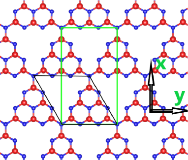
The structure of the monolayer g- is illustrated in Figure 1, which shows a large aperture and a triazine ring as a unit. Firstly, the optimized lattice constants of monolayer g- is ==7.134 using GGA, which agrees well with previous theoretical and experimental valuesm1 ; c5 . The band structure of the g- monolayer using HSE06 is calculated, which shows an indirect band gap semiconductor with the valence band maximum (VBM) at point and the conduction band minimum (CBM) at K point. The position of CBM is different from previous one (at M point)m1 , which may be due to different HSE06 parameters. The calculated HSE06 band gap is 2.77 eV, which is very close to the experimental value (2.7 eV)c5 and the previous calculated result (2.76 eV)m1 . The independent elastic stiffness coefficients of and are calculated, and the monolayer has constants of =184.92 and =48.02 , which meet the Born criteria of mechanical stability. These elastic constants are larger than ones of q9 ; q11 . The 2D Young s moduli and shear modulus can be expressed asela :
| (8) |
| (9) |
| (10) |
The corresponding Poisson’s ratios is given:
| (11) |
The calculated values are =172.45 , =68.45 and =0.26. The related data of g- monolayer are listed in Table 1.
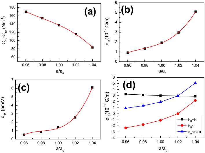
The rectangle supercell is used to calculate piezoelectric stress coefficients of g- monolayer by DFPT, and the x and y directions are shown in Figure 1. The calculated piezoelectric coefficient =1.94 C/m, being close to previous value =2.18 C/mnc . It is found that the electronic contribution is opposite to ionic contribution, and they are 3.02 C/m and -1.08 C/m, respectively. Based on calculated , and , the predicted is 1.42 pm/V, which is smaller than most 2D TMD monolayersq11 . Strain strategy is an effective method to improve piezoelectric effect of 2D materialsq7-1 ; r1 ; r3 . Here, we only consider biaxial strain, which can not produce polarization, not like uniaxial strain. In the simulation, the small biaxial strain (-4% to 4%) effects on piezoelectric properties of monolayer g- are studied, which may be easily achieved in experiment. The elastic constants -, piezoelectric coefficients and as a function of biaxial strain are plotted in Figure 2. It is clearly seen that the - decreases, and increases, when the strain changes from -4% to 4%. This will lead to improved according to Equation 7 with 4% to 4% strain. At 4% strain, the becomes 6.12 pm/V from unstrained 1.42 pm/V, increased by 331%.
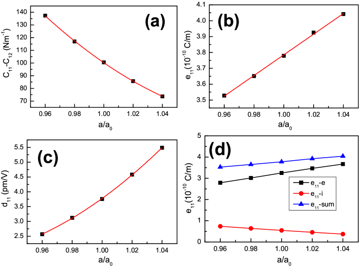
The ionic contribution and electronic contribution to as a function of biaxial strain are also plotted in Figure 2. It is found that there are narrow variations for electronic contribution with -4% to 4% strain, and only varies -0.35 C/m. However, the magnitude change of the ionic contribution is very large, and about 4.52 C/m. Therefore, the ionic contribution has an important role to enhance piezoelectric effect of g- monolayer caused by strain, which is different from a typical 2D piezoelectric material . The monolayer has the same point group with g-, which gives rise to the same reduced piezoelectric coefficients. The elastic constants -, piezoelectric coefficients and , and the ionic contribution and electronic contribution to of monolayer as a function of biaxial strain are plotted in Figure 3. For unstrained , our calculated (131.76 ), (31.20 ), (3.78 C/m) and (3.76 pm/V) agree well with previous theoretical values (130 , 32 , 3.64 C/m, 3.73 pm/V)q11 . For -, and , the change trend is similar to one of g- with strain changing from -4% to 4%. However, the electronic part has positive contribution to improve piezoelectric effect of , while the ionic part gives negative effect. Thus, the electronic part dominate the enhancement of piezoelectric effect of monolayer caused by strain.
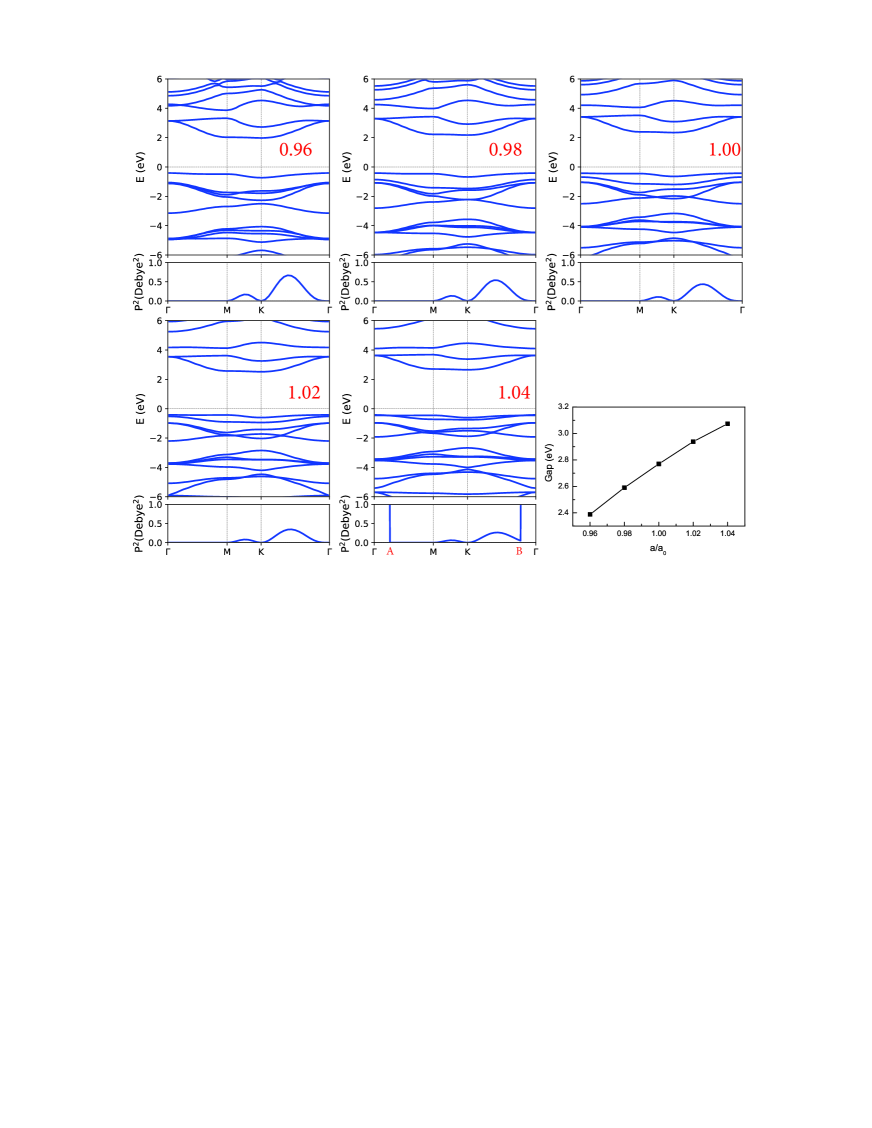
The monolayer g- at applied strain, exhibiting piezoelectricity, not only should break inversion symmetry, but also should have a band gap. To confirm strained g- to be a semiconductor, the energy band structures and gaps using HSE06 as a function of strain are plotted in Figure 4. It is clearly seen that the gap increases from 2.39 eV (-4%) to 3.07 eV (4%), but the positions of VBM and CBM do not change. It is found that the strain can induce the cross between the first and second valence bands at about 4% strain, which produces important effect on TDM. The TDM is the electric dipole moment associated with the transition between the two states, and we calculate the squares of TDM from the highest valence band to the lowest conduction band, which is also shown in Figure 4. The calculated results show that the outline of TDM has little change from -4% to 2%, which are mainly along -K and K-M. However, the magnitude of TDM becomes huge along -A and -B at 4% strain because of band cross between the first and second valence bands. So, strain can also produce important influence on optical absorptions of monolayer g-.
V Conclusion
In summary, the reliable first-principles calculations are performed to investigate the biaxial strain (-4%-4%) effects on piezoelectric properties in monolayer g-. Compared to unstrain one, compressive strain reduces , and increases -. However, tensile strain produces opposite effects on and -. These lead to improved from compressive strain to tensile one. Calculated results show that the ionic contribution to of g- is in favour of the strain-induced enhanced , which is different from monolayer. It is found that the HSE06 gap increases from 2.39 eV (-4%) to 3.07 ev (4%). The tensile strain (4%) can induce the cross between the first and second valence bands, which can induce huge TDM. Our predictive findings can provide a simple way to achieve energy-efficient energy transformation devices.
Acknowledgements.
This work is supported by the Natural Science Foundation of Shaanxi Provincial Department of Education (19JK0809). We are grateful to the Advanced Analysis and Computation Center of China University of Mining and Technology (CUMT) for the award of CPU hours and WIEN2k/VASP software to accomplish this work.References
- (1) P. Niu, L. L. Zhang, G. Liu and H. M. Cheng, Adv. Funct. Mater. 22, 4763 (2012).
- (2) S. B. Yang, Y. J. Gong, J. S. Zhang, L. Zhan, L. L. Ma, Z. Y. Fang, R. Vajtai, X. C. Wang and P. M. Ajayan, Adv. Mater. 25, 2452 (2013).
- (3) T. Y. Ma, Y. H. Tang, S. Dai and S. Z. Qiao, Small 10, 2382 (2014).
- (4) F. Zhao, H. H. Cheng, Y. Hu, L. Song, Z. P. Zhang, L. Jiang and L. T. Qu, Sci. Rep. 4, 5882 (2014).
- (5) X. Wang, K. Maeda, A. Thomas, K. Takanabe, G. Xin, J. M. Carlsson, K. Domen and M. Antonietti, Nat. Mater. 8, 76 (2009).
- (6) Y. Hou, A. B. Laursen, J. Zhang, G. Zhang, Y. Zhu, X. Wang et al., Angew. Chem., Int. Ed. 52, 3621 (2013).
- (7) J. W. Zhou, M. Zhang and Y. F. Zhu, Phys. Chem. Chem. Phys. 17, 3647 (2015).
- (8) J. Fu, B. B Chang,Y. L. Tian, F. N. Xi and X. P. Dong, J. Mater. Chem. A 1, 3083 (2013).
- (9) W. Wu and Z. L. Wang, Nat. Rev. Mater. 1, 16031 (2016).
- (10) W. Wu, L. Wang, Y. Li, F. Zhang, L. Lin, S. Niu, D. Chenet, X. Zhang, Y. Hao, T. F. Heinz, J. Hone and Z. L. Wang, Nature 514, 470 (2014).
- (11) H. Zhu, Y. Wang, J. Xiao, M. Liu, S. Xiong, Z. J. Wong, Z. Ye, Y. Ye, X. Yin and X. Zhang, Nat. Nanotechnol. 10, 151 (2015).
- (12) A. Y. Lu, H. Zhu, J. Xiao, C. P. Chuu, Y. Han, M. H. Chiu, C. C. Cheng, C. W. Yang, K. H. Wei, Y. Yang, Y. Wang, D. Sokaras, D. Nordlund, P. Yang, D. A. Muller, M. Y. Chou, X. Zhang and L. J. Li, Nat. Nanotechnol. 12, 744 (2017).
- (13) L. Dong, J. Lou and V. B. Shenoy, ACS Nano, 11, 8242 (2017).
- (14) S. D. Guo, X. S. Guo, Y. Y. Zhang and K. Luo, J. Alloy. Compd. 822, 153577 (2020).
- (15) S. D. Guo, X. S. Guo, R. Y. Han and Y. Deng, Phys. Chem. Chem. Phys. 21, 24620 (2019).
- (16) S. D. Guo, X. S. Guo, Z. Y. Liu and Y. N. Quan, J. Appl. Phys. 127, 064302 (2020).
- (17) S. D. Guo and S. Q. Wang, J. Phys. Chem. Solids 140, 109375 (2020).
- (18) M. N. Blonsky, H. L. Zhuang, A. K. Singh and R. G. Hennig, ACS Nano, 9, 9885 (2015).
- (19) R. X. Fei, We. B. Li, J. Li and L. Yang, Appl. Phys. Lett. 107, 173104 (2015)
- (20) K. N. Duerloo, M. T. Ong and E. J. Reed, J. Phys. Chem. Lett. 3, 2871 (2012).
- (21) Y. Chen, J. Y. Liu, J. B. Yu, Y. G. Guo and Q. Sun, Phys. Chem. Chem. Phys. 21, 1207 (2019).
- (22) Y. G. Guo, H. Q. Zhu and Q. Wang, ACS Appl. Mater. Interfaces 11, 1033 (2019).
- (23) N. Jena, Dimple, S. D. Behere and A. D. Sarkar, J. Phys. Chem. C 121, 9181 (2017).
- (24) Dimple, N. Jena, A. Rawat, R. Ahammed, M. K. Mohanta and A. D. Sarkar, J. Mater. Chem. A 6, 24885 (2018).
- (25) X. Wu, D. Vanderbilt and D. R. Hamann, Phys. Rev. B 72, 035105 (2005).
- (26) P. Hohenberg and W. Kohn, Phys. Rev. 136, B864 (1964); W. Kohn and L. J. Sham, Phys. Rev. 140, A1133 (1965).
- (27) G. Kresse, J. Non-Cryst. Solids 193, 222 (1995).
- (28) G. Kresse and J. Furthmller, Comput. Mater. Sci. 6, 15 (1996).
- (29) G. Kresse and D. Joubert, Phys. Rev. B 59, 1758 (1999).
- (30) J. P. Perdew, K. Burke and M. Ernzerhof, Phys. Rev. Lett. 77, 3865 (1996).
- (31) V. Wang, N. Xu, J. C. Liu, G. Tang and W. T. Geng, arXiv:1908.08269v4 (2019).
- (32) J. J. Liu, J. Phys. Chem. C 119, 28417 (2015).
- (33) R. C. Andrew, R. E. Mapasha, A. M. Ukpong and N. Chetty, Phys. Rev. B 85, 125428 (2012).
- (34) M. Zelisko, Y. Hanlumyuang, S. B. Yang, Y. M. Liu, C. H. Lei, J. Y. Li, P. M. Ajayan and P. Sharma, Nat. Commun. 5, 4284 (2014).