Terahertz photoresistivity of a high-mobility 3D topological insulator based on a strained HgTe film
Abstract
We report on a detailed study of the terahertz (THz) photoresistivity in a strained HgTe three-dimensional topological insulator (3D TI) for all Fermi level positions: inside the conduction and valence bands, and in the bulk gap. In the presence of a magnetic field we detect a resonance corresponding to the cyclotron resonance (CR) in the top surface Dirac fermions (DF) and examine the nontrivial dependence of the surface state cyclotron mass on the Fermi level position. We also detect additional resonant features at moderate electron densities and demonstrate that they are caused by the mixing of surface DF and bulk electrons. At high electron densities, we observe THz radiation induced -periodic low-field magneto-oscillations coupled to harmonics of the CR and demonstrate that they have a common origin with microwave-induced resistance oscillations (MIRO) previously observed in high mobility GaAs-based heterostructures. This observation attests the superior quality of 2D electron system formed by helical surface states in strained HgTe films.
Three-dimensional TIs based on strained HgTe films have been the subject of an intensive study in the last ten years. This system is a strong topological insulator with electronic properties mediated by conducting surface helical states with close to linear dispersion with spins locked to the electron’s momentum Fu and Kane (2007); Dai et al. (2008) and is characterized by a very high mobility of the surface DF, reaching cm2/Vs in these systems, and low bulk conductivity. The properties of the surface states have been comprehensively studied using magneto-transport, phase-sensitive SQUID and capacitance spectroscopy Brüne et al. (2011); Kozlov et al. (2014); Brüne et al. (2014); Maier et al. (2015); Kozlov et al. (2016); Maier et al. (2017); Thomas et al. (2017); Ziegler et al. (2018); Noel et al. (2018); Ziegler et al. (2020). These experiments resulted in the observation of the quantum Hall effect and probing of quantum capacitance in a 3D topological insulator, demonstrated a non-trivial Berry phase of Shubnikov – de Haas oscillations in transport and capacitance responses, provided an access to a detailed study of the surface states transport properties, and demonstrated highly efficient spin-to-charge current conversion. Presence of the topologically protected conducting surface states in strained HgTe 3D TIs also gives rise to a number of phenomena driven by THz electric fields. Observation of universal Faraday and Kerr effects Shuvaev et al. (2012); Dziom et al. (2017) predicted in Ref. Tse and MacDonald, 2010; THz quantum Hall effect Shuvaev et al. (2013) and photogalvanic currents Dantscher et al. (2015); Candussio et al. (2019) excited in the surface states; study of surface states dynamic applying time domain spectroscopy Hancock et al. (2011) and cyclotron resonance spectroscopy Shuvaev et al. (2013); Dantscher et al. (2015); Candussio et al. (2019); Gospodarič et al. (2019); Gospodaric2020, where values of the effective mass of DF from top and bottom surfaces were determined, are only some examples of the achievements in this field.
While THz radiation induced optical and photocurrent phenomena have been widely investigated there has been no work so far aimed at the study of the photoconductive (photoresistive) response of the surface states. Such measurements in 3D TI, however, would not only yield information on tiny details of carrier scattering mechanisms and CR (for HgTe 2D systems see Ref. Otteneder et al., 2018) but also may result in the observation of such fascinating phenomena as MIRO previously detected in 2D systems with parabolic dispersion Zudov et al. (2001); Dmitriev et al. (2012) and, most recently, in DF in graphene Mönch et al. (2020).
In this paper we report on the investigation of the THz photoresistance of HgTe-based 3D TIs for all Fermi level, , positions: inside the conduction and valence bands, and in the bulk energy gap. Studying the magnetic field dependences of the photoresponse we observed pronounced CR and, at high electron densities, THz radiation induced MIRO-like oscillations coupled to CR. Furthermore, for the intermediate electron densities we detected an additional set of oscillations which behave similarly to magneto-intersubband oscillations (MISO) detected in coupled double quantum wells (QWs) Bykov et al. (2008); Wiedmann et al. (2008).
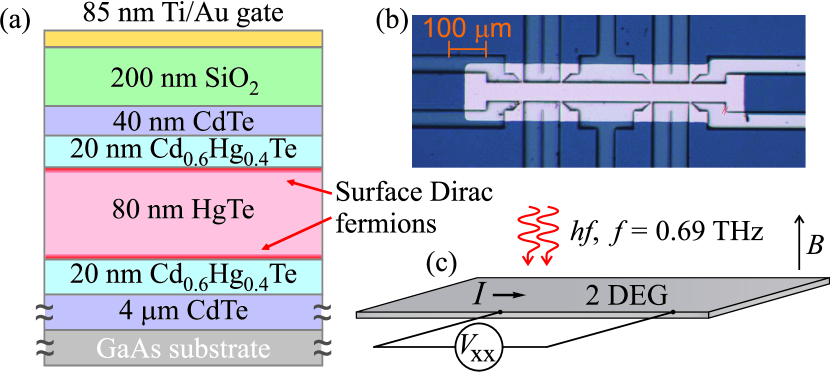
Experimental samples are field effect transistor-like Hall-bar structures with semi-transparent Ti/Au gates fabricated on the basis of strained 80-nm HgTe films that have been grown by molecular beam epitaxy on a GaAs (013) substrate Kozlov et al. (2014) (Fig. 1). The Hall-bar channel width is 50 and distances between potential probes are 100 and 250 . The samples are placed into an optical cryostat. We apply a molecular far-infrared laser as a source of THz radiation with frequency THz (wavelength ) Kvon et al. (2008); Olbrich et al. (2013); Olbrich2016. The incident power mW is modulated at about 160 Hz by an optical chopper. Photoresistance is measured by means of a double modulation technique Kozlov et al. (2011) with a low modulation frequency of 6 Hz and a high one corresponding to the chopper frequency. The temperature range of the experiment is K.
All studied samples have been characterized by magnetotransport measurements using a standard low-frequency lock-in technique in a perpendicular magnetic field B up to 7 T and current I in the range of nA. Typical gate voltage dependences of dissipative, , and Hall, , resistivities are shown in Fig. 2 (b) and (c). The values of gate voltage corresponding to the conduction band bottom () and the valence band top (), see marked arrows in Fig. 2, were determined following the methods developed in Refs. Kozlov et al., 2014 and Ziegler et al., 2018. Specifically, the electron-hole scattering, activated by temperature, results in a sharp rise of the zero-field resistivity when enters the valence band, see Fig. 2 (b). The low-field magnetoresistance, see Fig. 2 (d), rapidly increases when enters either the conduction or valence band, reflecting the simultaneous presence of two different types of carriers.
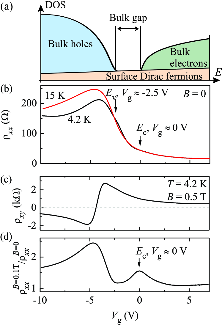
Fig. 3 (a) demonstrates the main result of our work – magnetic field dependences of the photoresistivity normalized to the maximum of its absolute value . The dependences are measured at for three ranges of corresponding to the Fermi level position in: i) the valence band (V), ii) in the gap (V), and iii) in the conduction band (). All curves are measured at 20 K. This temperature is high enough to suppress the contribution of the Shubnikov – de Haas oscillations. One can clearly see that dependences have resonant shapes with the maximum position lying in the magnetic field range T depending on the applied gate voltage, i.e., Fermi level position. Using the value of one can determine the cyclotron effective mass , where is the elementary charge. In Fig. 3 (b) we show the gate voltage dependence of . One can see that this dependence has a nonmonotonic behavior with a minimum value of near the valence band top; is the free electron mass. The cyclotron mass approaches its maximum value at the highest gate voltages, corresponding to a DF density of about cm-2. In fact, such nonmonotonic behavior of the cyclotron mass and its values are in line to what was measured Shuvaev et al. (2012); Dantscher et al. (2015); Gospodarič et al. (2019), and calculated Dantscher et al. (2015); Gospodarič et al. (2019) for surface DF in HgTe.
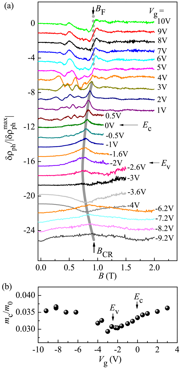
Measurements of the temperature dependence of the dark resistance at different gate voltages demonstrate that the change of sign of the CR photoresistivity around V in Fig. 3 is accompanied by the sign change in the correspondent temperature variations of the dark resistivity (see supplementary material). These observations provide a strong support to the conventional heating mechanism of the observed CR photoresistivity. The photoresistivity in this case can be expressed as
| (1) |
where is a positive coefficient relating the incident power to the increase of the temperature of DF, and is the absorption coefficient.
Now we analyze the shape of the CR photoresistivity. We begin from a gate voltage range corresponding to the Fermi level positions in the valence band (see Fig. 4 (a)). In this range the photoresistivity is quite satisfactory fitted by a Lorentzian curve. It is interesting to compare the Lorentzian width with the theoretical CR width for separated Landau levels using an expression for the latter in the case of a short range potential Ando, Fowler, and Stern (1982); Dmitriev et al. (2012)
| (2) |
where is the cyclotron frequency and is the relaxation time. In the valence band the DF mobility is about cm2/Vs which corresponds to meV. This value is two to three times larger compared to experimental resonance width values. A possible origin of the indicated discrepancy is the inelastic scattering of surface DF by bulk holes which is very significant in the temperature range we used in our experiments Kozlov et al. (2014).
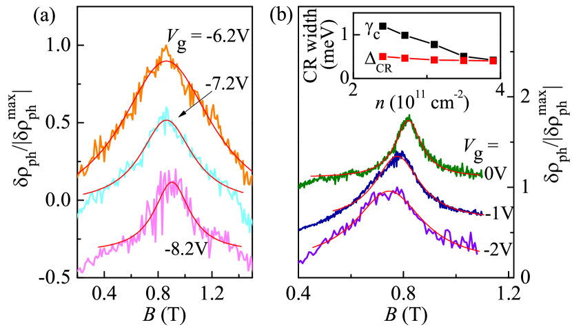
Next we consider the CR photoresistivity shape when the Fermi level enters into the gap (Fig. 4 (b)). The fitting of the photoresistivity by a Lorentzian function also demonstrates quite good agreement. It gives a resonance width of about 0.3 T when the Fermi level lies near the top of the valence band, and it decreases when the Fermi level moves to the bottom of the conduction band. More careful analysis of the behavior shows an interesting feature (inset to Fig. 4 (b)): as the Fermi level moves through the gap from the valence band top to the conduction band bottom a significant CR peak narrowing occurs, while has no change.
As the Fermi level leaves the gap and enters the conduction band (see a dependence in Fig. 3 (a) at V) photoresistivity oscillations at magnetic fields below emerge. Note that these oscillations are absent when the Fermi level intersects only the surface states. Since the top surface DF have higher density and mobility in the studied systems Kozlov et al. (2014, 2016), the oscillations are presumably generated by the mixing of a top surface DF band and the bulk conduction band, which, more accurately, contains a set of the size-quantized subbands Brüne et al. (2011); Dantscher et al. (2015). So the observed oscillations are similar to magnetointersubband oscillations (MISO) in coupled double QWs studied in Ref. Bykov et al., 2008; Wiedmann et al., 2008. But in our case we have two significantly different sets of interacted bands: the spin-polarized surface DF band and the size-quantized subbands of the 80 nm HgTe film. Moreover, in our experiment we have an important advantage: due to the field effect transistor structure we are able to change the position of the Fermi level and correspondingly the subband densities. The absence of MISO at negative voltages is attributed to the much lower mobility and dense spectrum of the bulk holes Dantscher et al. (2015).
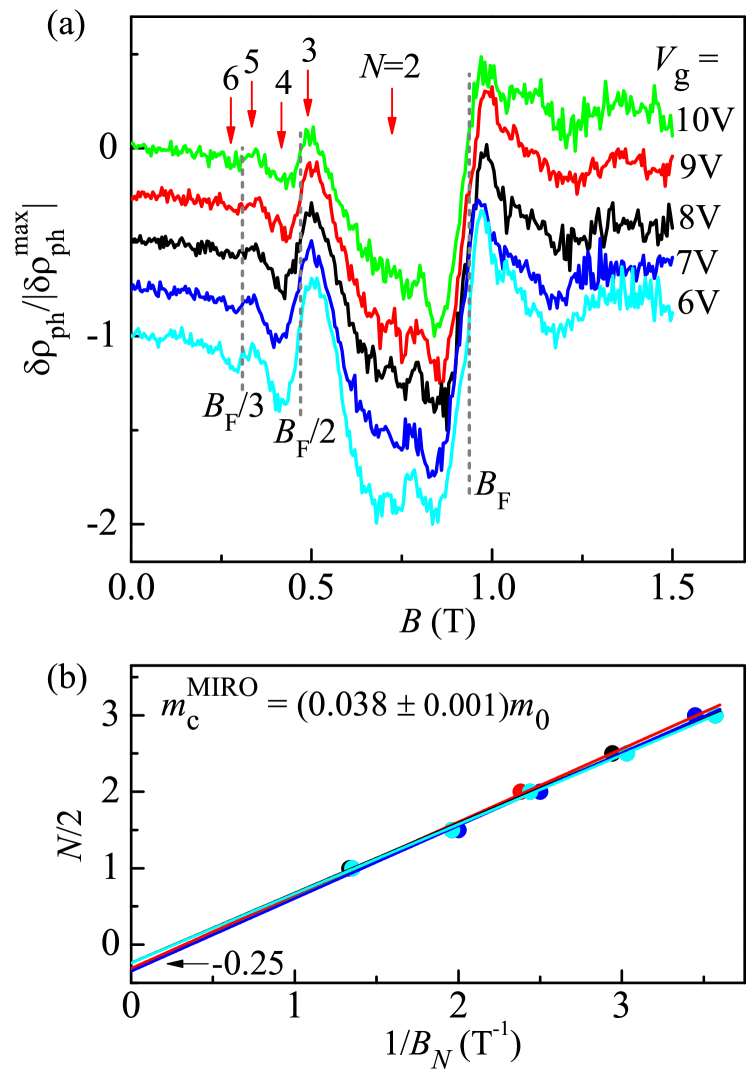
As the Fermi level moves further inside the conduction band, these oscillations are superimposed with THz induced MIRO-like oscillations that have nearly the same structure for several gate voltages ranging from 6 to 10 V, see Fig. 5 (a). The emergence of MIRO in the photoresistivity at high electron densities is consistent with results of previous studies in different materials Dmitriev et al. (2012); Tabrea2020; Mönch et al. (2020). Arrows in Fig. 5 (a) show the positions of subsequent extrema of MIRO, numbered as . It is well known that for MIRO Dmitriev et al. (2012)
| (3) |
where . Thereby, the slope of the v.s. dependence, see Fig. 5 (b), is equal to that allows us to determine the corresponding effective mass . This value is close to the cyclotron mass values at high positive , where it is possible to mark out CR ( and 3 V). We note that approximation lines start near as it is established for MIRO Dmitriev et al. (2012). A detailed study of the observed transformation of the photoresistance from one CR peak to MIRO-like oscillations through a rich picture of interband interaction induced oscillations will be reported later.
To conclude, we have observed and studied the THz photoresistivity of 80-nm-thick strained HgTe 3D TI. The photoresistivity was studied at all Fermi level positions: inside the conduction and valence bands and in the bulk gap. For the Fermi level lying in the valence band or the gap, we observed a single resonance of the photoresistivity, which is caused by the cyclotron resonance of DF in the top surface. For higher positions of the Fermi level, i.e, for lying in the conduction band, the CR-photoresistivity becomes superimposed fist with magnetointersubband oscillations, and, at further increase of , with MIRO oscillations. The observation of MIRO provides an important evidence of high quality of 2D electron system formed by helical surface states in strained HgTe films.
Supplementary material
See the Supplementary Material bellow. Content: magnetic field dependencies of the resistivity measured at different gate voltages and temperatures.
Acknowledgements.
We are grateful to Dima Kozlov for discussions. Novosibirsk team acknowledges the financial support by the Russian Science Foundation (Grant No. 16-12-10041-P). Regensburg team gratefully acknowledges the support of the Deutsche Forschungsgemeinschaft (DFG) - Project-ID 314695032 - SFB 1277, and the Volkswagen Stiftung Program (97738). S.D.G. also thanks the IRAP program of the Foundation for Polish Science (grant MAB/2018/9, CENTERA) for the support.Data availability
The data that support the findings of this study are available from the corresponding authors upon reasonable request.
References
- Fu and Kane (2007) L. Fu and C. L. Kane, Phys. Rev. B 76, 045302 (2007).
- Dai et al. (2008) X. Dai, T. L. Hughes, X. L. Qi, Z. Fang, and S. C. Zhang, Phys. Rev. B 77, 125319 (2008).
- Brüne et al. (2011) C. Brüne, C. X. Liu, E. G. Novik, E. M. Hankiewicz, H. Buhmann, Y. L. Chen, X. L. Qi, Z. X. Shen, S. C. Zhang, and L. W. Molenkamp, Phys. Rev. Lett. 106, 126803 (2011).
- Kozlov et al. (2014) D. A. Kozlov, Z. D. Kvon, E. B. Olshanetsky, N. N. Mikhailov, S. A. Dvoretsky, and D. Weiss, Phys. Rev. Lett. 112, 196801 (2014).
- Brüne et al. (2014) C. Brüne, C. Thienel, M. Stuiber, J. Bottcher, H. Buhmann, E. G. Novik, C.-X. Liu, E. M. Hankiewicz, and L. W. Molenkamp, Phys. Rev. X 4, 041045 (2014).
- Maier et al. (2015) L. Maier, E. Bocquillon, M. Grimm, J. B. Oostinga, C. Ames, C. Gould, C. Brüne, H. Buhmann, and L. W. Molenkamp, Phys. Scr. T164, 014002 (2015).
- Kozlov et al. (2016) D. A. Kozlov, D. Bauer, J. Ziegler, R. Fischer, M. L. Savchenko, Z. D. Kvon, N. N. Mikhailov, S. A. Dvoretsky, and D. Weiss, Phys. Rev. Lett. 116, 166802 (2016).
- Maier et al. (2017) H. Maier, J. Ziegler, R. Fischer, D. Kozlov, Z. D. Kvon, N. Mikhailov, S. A. Dvoretsky, and D. Weiss, Nat. Commun. 8, 2023 (2017).
- Thomas et al. (2017) C. Thomas, O. Crauste, B. Haas, P.-H. Jouneau, C. Bäuerle, L. P. Lévy, E. Orignac, D. Carpentier, P. Ballet, and T. Meunier, Phys. Rev. B 96, 245420 (2017).
- Ziegler et al. (2018) J. Ziegler, R. Kozlovsky, C. Gorini, M.-H. Liu, S. Weishäupl, H. Maier, R. Fischer, D. A. Kozlov, Z. D. Kvon, N. Mikhailov, S. A. Dvoretsky, K. Richter, and D. Weiss, Phys. Rev. B 97, 035157 (2018).
- Noel et al. (2018) P. Noel, C. Thomas, Y. Fu, L. Vila, B. Haas, P.-H. Jouneau, S. Gambarelli, T. Meunier, P. Ballet, and J. P. Attané, Phys. Rev. Lett. 120, 167201 (2018).
- Ziegler et al. (2020) J. Ziegler, D. A. Kozlov, N. N. Mikhailov, S. Dvoretsky, and D. Weiss, Phys. Rev. Res. 2, 033003 (2020).
- Shuvaev et al. (2012) A. M. Shuvaev, G. V. Astakhov, C. Brüne, H. Buhmann, L. W. Molenkamp, and A. Pimenov, Semicond. Sci. Technol. 27, 124004 (2012).
- Dziom et al. (2017) V. Dziom, A. Shuvaev, A. Pimenov, G. V. Astakhov, C. Ames, K. Bendias, J. Böttcher, G. Tkachov, E. M. Hankiewicz, C. Brüne, H. Buhmann, and L. W. Molenkamp, Nat. Commun. 8, 15197 (2017).
- Tse and MacDonald (2010) W.-K. Tse and A. H. MacDonald, Phys. Rev. Lett. 105, 057401 (2010).
- Shuvaev et al. (2013) A. M. Shuvaev, G. V. Astakhov, G. Tkachov, C. Brüne, H. Buhmann, L. W. Molenkamp, and A. Pimenov, Phys. Rev. B 87, 121104(R) (2013).
- Dantscher et al. (2015) K.-M. Dantscher, D. A. Kozlov, P. Olbrich, C. Zoth, P. Faltermeier, M. Lindner, G. V. Budkin, S. A. Tarasenko, V. V. Bel’kov, Z. D. Kvon, N. N. Mikhailov, S. A. Dvoretsky, D. Weiss, B. Jenichen, and S. D. Ganichev, Phys. Rev. B 92, 165314 (2015).
- Candussio et al. (2019) S. Candussio, G. V. Budkin, M. Otteneder, D. A. Kozlov, I. A. Dmitriev, V. V. Bel’kov, Z. D. Kvon, N. N. Mikhailov, S. A. Dvoretsky, and S. D. Ganichev, Phys. Rev. Mater. 3, 054205 (2019).
- Hancock et al. (2011) J. N. Hancock, J. L. M. van Mechelen, A. B. Kuzmenko, D. van der Marel, C. Brüne, E. G. Novik, G. V. Astakhov, H. Buhmann, and L. W. Molenkamp, Phys. Rev. Lett. 107, 136803 (2011).
- Gospodarič et al. (2019) J. Gospodarič, V. Dziom, A. Shuvaev, A. A. Dobretsova, N. N. Mikhailov, Z. D. Kvon, and A. Pimenov, Phys. Rev. B 99, 115130 (2019).
- Otteneder et al. (2018) M. Otteneder, I. A. Dmitriev, S. Candussio, M. L. Savchenko, D. A. Kozlov, V. V. Bel’kov, Z. D. Kvon, N. N. Mikhailov, S. A. Dvoretsky, and S. D. Ganichev, Phys. Rev. B 98, 245304 (2018).
- Zudov et al. (2001) M. A. Zudov, R. R. Du, J. A. Simmons, and J. L. Reno, Phys. Rev. B 64, 201311 (2001).
- Dmitriev et al. (2012) I. A. Dmitriev, A. D. Mirlin, D. G. Polyakov, and M. A. Zudov, Rev. Mod. Phys. 84, 1709 (2012).
- Mönch et al. (2020) E. Mönch, D. A. Bandurin, I. A. Dmitriev, I. Y. Phinney, I. Yahniuk, T. Taniguchi, K. Watanabe, P. Jarillo-Herrero, and S. D. Ganichev, Nano Lett. 20, 5943 (2020).
- Bykov et al. (2008) A. A. Bykov, D. R. Islamov, A. V. Goran, and A. I. Toropov, JETP Lett. 87, 477 (2008).
- Wiedmann et al. (2008) S. Wiedmann, G. M. Gusev, O. E. Raichev, T. E. Lamas, A. K. Bakarov, and J. C. Portal, Phys. Rev. B 78, 121301 (2008).
- Kvon et al. (2008) Z.-D. Kvon, S. N. Danilov, N. N. Mikhailov, S. A. Dvoretsky, W. Prettl, and S. D. Ganichev, Phys. E 40, 1885 (2008).
- Olbrich et al. (2013) P. Olbrich, C. Zoth, P. Vierling, K.-M. Dantscher, G. V. Budkin, S. A. Tarasenko, V. V. Bel’kov, D. A. Kozlov, Z. D. Kvon, N. N. Mikhailov, S. A. Dvoretsky, and S. D. Ganichev, Phys. Rev. B 87, 235439 (2013).
- Kozlov et al. (2011) D. A. Kozlov, Z. D. Kvon, N. N. Mikhailov, S. A. Dvoretskii, and J. C. Portal, JETP Lett. 93, 170 (2011).
- Ando, Fowler, and Stern (1982) T. Ando, A. B. Fowler, and F. Stern, Rev. Mod. Phys. 54, 437 (1982).