Direct observation and evolution of electronic coupling between organic semiconductors
Abstract
The electronic wavefunctions of an atom or molecule are affected by its interactions with its environment. These interactions dictate electronic and optical processes at interfaces, and is especially relevant in the case of thin film optoelectronic devices such as organic solar cells. In these devices, charge transport and interfaces between multiple layers occur along the thickness or vertical direction, and thus such electronic interactions between different molecules – same or different – are crucial in determining the device properties. Here, we introduce a new in-situ spectroscopic ellipsometry data analysis method called DART with the ability to directly probe electronic coupling due to intermolecular interactions along the thickness direction using vacuum-deposited organic semiconductor thin films as a model system. The analysis, which does not require any model fitting, reveals direct observations of electronic coupling between frontier orbitals under optical excitations leading to delocalization of the corresponding electronic wavefunctions with thickness or, equivalently, number of molecules away from the interface in C60 and MeO-TPD deposited on an insulating substrate (SiO2). Applying the same methodology for C60 deposited on phthalocyanine thin films, the analyses shows strong, anomalous features – in comparison to C60 deposited on SiO2 – of the electronic wavefunctions corresponding to specific excitation energies in C60 and phthalocyanines. Translation of such interactions in terms of dielectric constants reveals plasmonic type resonance absorptions resulting from oscillations of the excited state wavefunctions between the two materials across the interface. Finally, reproducibility, angstrom-level sensitivity and simplicity of the method are highlighted showcasing its applicability for studying electronic coupling between any vapor-deposited material systems where real-time measurements during thin film growth are possible.
I INTRODUCTION
The electronic wavefunctions of an atom in a solid depend on the positions of the electrons and the nuclei. Changes in the energy levels occur due to the overlap of the ground state electronic wavefunctions primarily of the frontier orbitals between neighboring atoms or molecules, and determines the optoelectronic properties of a solid, e.g. leading to the emergence of bands in semiconductors Ashcroft and Mermin (1976); Simon (2013). Understanding how the energy levels in an atom evolve from isolation to a many-atom solid is one of the most important fundamentals of solid state physics required for explaining the properties of solids such as metals, semiconductors and insulators.
In the case of organic semiconductors, comprised typically of large molecules, understanding the effects of intermolecular interactions on the electronic wavefunctions is crucial for understanding the physics at interfaces since the interfacial phenomena, e.g. transfer of a charge between a donor and an acceptor in solar cells, are affected by the local environment Azzouzi et al. (2018); Eisner et al. (2019); Athanasopoulos et al. (2019); Kahle et al. (2018); Menke et al. (2018); Gélinas et al. (2014) to which the frontier orbitals react. This is relevant not just for organic semiconductors but any electronic material such as conductive oxides, chalcogenides and metals forming the layers of optoelectronic thin film devices where interfacial processes play a critical role in the device properties, and especially more in the case of vertical devices (where charge transport occurs along the thickness direction in contrast to thin film field-effect transistors).
In-situ optical spectroscopic techniques such as in-situ differential reflectance spectroscopy (DRS) Forker et al. (2012); Gruenewald et al. (2016) and reflection anisotropy spectroscopy (RAS) Aspnes and Studna (1985); Martin and Weightman (2004); Bussetti et al. (2009) have been around for many years and offer a non-destructive way of probing such intermolecular interactions. In-situ DRS has been used to study electronic coupling and its evolution with thickness, for example, between flat-lying tin(II)-phthalocyanine (SnPc) molecules Gruenewald et al. (2016) and between quaterrylene molecules Forker et al. (2012) deposited under vacuum. These works demonstrate the strength of in-situ optical spectroscopic techniques, but also one of the current limitations of DRS and RAS. While it is possible to infer electronic coupling in the perpendicular direction, for example, between quaterrylene molecules and the underlying gold layer (as a metal substrate) Forker et al. (2012), due to the near-normal incidence of the probe light in DRS (and in RAS), the data obtained is primarily that of the in-plane component of the dielectric constants Forker et al. (2012) since the orientation of the electric field of the probe light is nearly all in the plane of the film. Being able to directly access the out-of-plane interactions of molecules would complement DRS/RAS and open up new avenues in probing and characterizing electronic coupling in interacting systems essential for further expanding the understanding of the physics of thin film optoelectronic devices. For example, in many organic electronic devices, key processes happen at planar interfaces parallel to the substrate, e.g. this is where the generation of free charge carriers happens in planar heterojunction organic solar cells.
One experimental technique which can probe this out-of-plane direction is in-situ spectroscopic ellipsometry (iSE), also sometimes referred to as "real-time" SE. This is possible firstly because of the high angle of incidence employed during measurements (typically 65∘). Secondly because of the use of polarized light, where the amplitude and phase change of the electric field upon interaction with the thin film are measured Fujiwara (2007); Azzam and Bashara (1977). The combination of these parameters carry more information than just the intensity measured in typical optical spectroscopic techniques, and which is also the most significant drawback of X-ray techniques where phase information is lost. Thus, SE is a thin film characterization technique typically used to characterize the primary optical excitations in terms of optical properties: dielectric constants or refractive indices which represent the quality of the thin films Fujiwara (2007); Azzam and Bashara (1977). In the case of organic solar cells, the technique is typically used to characterize the active layers for understanding structure-property relationships Hinrichs et al. (2012); Yokoyama (2011); Klein et al. (2015); Schünemann et al. (2013), and for optical simulations to model absorption profiles within a device Burkhard et al. (2010).
iSE is an advanced application of SE which makes it possible to study the growth and evolution of the optical properties of multi-layered thin films, e.g. semiconductors deposited by thermal evaporation under vacuum or other vapor-deposition methods Yokoyama and Adachi (2010); Ye et al. (2020); Heitz and Drévillon (1998). (i)SE, in general, has an angstrom-level sensitivity towards changes in thicknesses. The standard SE analysis procedure, or SSE in short, for obtaining optical properties from the iSE data relies on fitting a dielectric function model (using, for example, Gaussian and Lorentzian functions) to the data, and the typical analysis is initiated with the assumption that the film has the same properties along its thickness Fujiwara (2007); Azzam and Bashara (1977). However, robust and confident in-depth analysis such as variation of dielectric constants along the thickness direction is not possible because of lack of additional data (only one angle of incidence in iSE against different angles of incidence as is possible in ex-situ SE including at normal incidence). Thus, the information obtained from SSE analysis is determined not only by the dielectric functions used during the fitting but also the type of model used to analyse single or multi-layered thin films. Moreover, from model fitting, even if any anomalies are seen in the dielectric constants especially along the growth direction due to interactions with other materials at the interfaces, the question of whether these anomalies are real or artifacts from fitting is posed. To ascertain the analysis, additional optical information such as about the in-plane dielectric constants obtained from in-situ DRS Forker et al. (2012); Gruenewald et al. (2016) is essential.
In this work, we present an experimental methodology using iSE coupled with a new data analysis method for studying the evolution of the electronic wavefunctions pertaining to the optical excitations along the thickness or vertical direction as a function of thickness or, equivalently, number of molecules in vacuum-deposited thin films. By an empirical comparison to the optical properties (n + j k), we show that the new iSE data analysis method extracts information representative of the same for every layer (thickness resolution down to 1 possible) deposited. The analysis does not involve any model fitting and is only based on tracking the differential change in the iSE data. Any changes in the electronic wavefunctions corresponding to the frontier orbitals under excitations due to overlap with that of the neighboring molecules - both same and different species – in the growth (thickness) direction is reflected in the information obtained from the analysis. We demonstrate the ability of the method by its application to the study of vacuum-deposited organic semiconductor thin films using fullerene (C60), boron subphthalocyanine chloride (SubPc), boron sub-2,3-naphthalocyanine chloride (SubNc) and N,N,N’,N’-Tetrakis-(4-methoxyphenyl)benzidine (MeO-TPD) on different underlying layers.
We also evaluate and discuss the implications of these observations by complementing the analysis with a systematic approach for obtaining dielectric constants along the thickness direction using SSE data analysis, i.e. model fitting. Moreover, we demonstrate the angstrom-level sensitivity, simplicity and reproducibility of the method. To the best of our knowledge, this is the first time such significant modulations in the optical response due to electronic coupling have been observed and the method reported. Finally, we conclude with the general applicability of this method for studying other systems where electronic coupling through intermolecular interactions are crucial.
II EXPERIMENTAL SECTION
The organic semiconductors SubPc (> 99%, Lumtec), SubNc (> 99%, Lumtec), C60 ( 99.999%, CreaPhys), molybdenum oxide (MoOx) (> 99.998%, Lumtec) and MeO-TPD (> 99%, Lumtec) were used as purchased. Substrates silicon wafer (with 23 nm SiO2 on top, purchased from J.A.Woollam, for calibrating the ellipsometer) and ultrasmooth quartz substrate (WZWOPTICAG) were cleaned with soap and deionized water, and then sonicated in acetone and isopropanol (in this order) at 50 ∘C for 20 minutes before drying with an air gun. Then the substrates were UV-ozone treated for 10 minutes and loaded into the vacuum chamber (CreaPhys) via a nitrogen glovebox. A Woollam RC2 spectroscopic ellipsometer was mounted at 65∘ angle of incidence onto the vacuum chamber. The thin films were deposited on the loaded substrates by thermal evaporation of the organic semiconductors (at rates 0.1-0.5 /s). The in-situ measurements (210-1690 nm or 0.7-5.9 eV) were carried out with an acquisition time which ranged from 4-10 s or measurement of data for every 1-2 increase in thickness.
Standard spectroscopic ellipsometry analysis (SSE) for deriving the refractive indices of each layer through model fitting to the data (and described in Section S2 in the supplementary information) was carried out in CompleteEASE software from J.A.Woollam company. Ex-situ SE data of some of the thin films after deposition was obtained, where required, at 55∘, 65∘ and 75∘ angles of incidence. The and time series values measured through CompleteEASE were exported into text format and analysed in python using the equation described in the Results and Discussion section.
III RESULTS AND DISCUSSION
III.1 DART
In standard SE measurements of thin films, the data measured are the electric field amplitude ratio and phase difference as a function of wavelength () or energy () of the probe light defined as the ellipsometric ratio Fujiwara (2007); Azzam and Bashara (1977)
| (1) |
During iSE, is measured as a function of time t or, equivalently, thickness d in the case of monitoring the growth of vacuum-deposited thin films, which in our case are organic semiconductors. A first derivative of Equation 1 with respect to time (or d) yields the following equation
| (2) |
When the time interval between measurements is constant, which is typically the case in in-situ measurements, Equation 2 simplifies to
| (3) |
where
| (4a) | |||
| (4b) | |||
The measured iSE data, and , can be numerically differentiated for and yielding at time t or thickness d.
iSE is a highly sensitive technique, sensitive to changes in the thickness direction of a surface Fujiwara (2007); Azzam and Bashara (1977) (also referred to as out-of-plane or z direction). In-plane/xy direction - probed in UV-visible absorption measurements - is defined as the plane of the film (see Figure S1). During iSE, the probe light passes through all the layers for every time point for which is measured. Since the thin film deposition or the direction of growth during iSE is along the z direction of the film, then is the rate of change of the optical response of the thin film, which is primarily a function of the change in the optical properties of the thin film in the z direction, namely out-of-plane refractive indices Nz (nz+j kz) or, equivalently, dielectric constants ( + j ). A basic derivation of in terms of Nxy (in-plane refractive indices of the film), Nz and d is given section S1 in the supplementary information. However, for a small, differential change in thickness , can also be interpreted as the optical response of the incoming layer that will be deposited on the substrate with the thin film at thickness d as exemplified in Figures 1 and 2. The following results are based on this method named as “Differential Analysis in Real Time” (DART).
III.2 C60 and MeO-TPD on SiO2
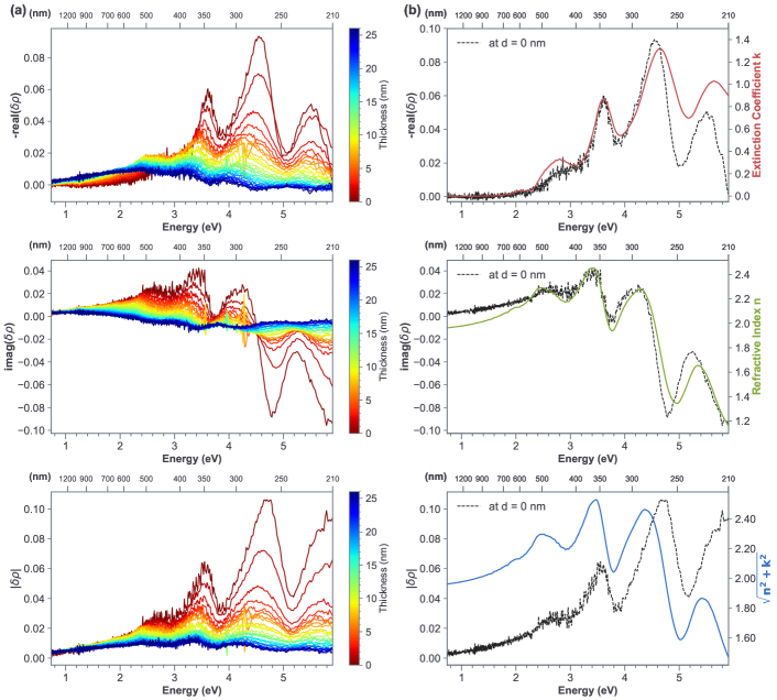
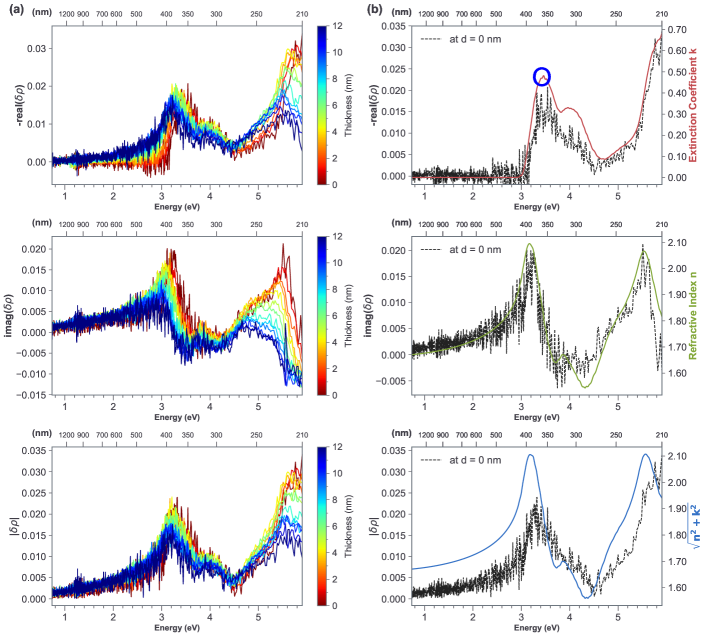
Figure 1(a) shows the real and imaginary parts as well as modulus of of C60 deposited on an optically smooth quartz substrate (SiO2); optically smooth implies that for the range of probe wavelengths (210-1690 nm), the roughness is on a sub-angstrom level. Thickness d of the film is obtained from SSE analysis (see Section S2). has been calculated for every 1 nm interval, i.e. = 1 nm, for all the data presented in this work. Firstly, to understand the meaning of real and imaginary values of , we compare ’s value calculated for the first layer deposited on a blank substrate, i.e. at d = 0 nm, to the k and n values of the C60 film (at 13 nm thickness) in Figure 1(b) obtained from SSE analysis using Gaussian functions (commonly referred to as oscillators). Such a function/oscillator can be used to fit to the absorption peaks which represent the sum of the main electronic transition and vibrionic progressions. Examining the profile of the first nanometer deposited, it can be seen that the -real() and imaginary() appear to represent k and n values respectively. The same observation can be seen for MeO-TPD (deposited on optically smooth quartz) in Figure 2. Thus, represents the optical properties of a layer , and its corresponding real (negative) and imaginary parts will be hereinafter referred to as and respectively.
SE probes the optical excitations of a system in terms of extinction coefficient k. Examining in Figure 1(a) for the first 1 nm layer, which can be approximated as a monolayer of C60 molecules that is deposited on a blank substrate (d = 0 nm), we observe that the strongest responses are centered at 3.6 eV, 4.6 eV and 5.5 eV, which correspond to the allowed, primary transitions T1u A1g with the strongest absorption in C60 Leach et al. (1992); Sassara et al. (2001); Lucas et al. (1992); Pavlovich and Shpilevsky (2010); Fukuda and Ehara (2012); also reflected in the extinction coefficient plot in Figure 1(b). This first nanometer data can be assumed as the average optical response of one C60 molecule deposited onto the SiO2 substrate. As more C60 deposits, we observe that the optical response is not the same for every additional nanometer being deposited. The magnitude gradually decreases and the peaks red-shift. This can be attributed to the intermolecular interactions between C60 molecules in the form of electronic coupling arising from overlap (along the thickness direction) of the frontier orbitals corresponding to the respective primary transitions in C60.
A consequence of this coupling is the delocalization of the corresponding electronic wavefunctions under excitation (or excited state wavefunctions) in C60 – a well-known phenomenon in C60 Bakulin et al. (2012); Burlingame et al. (2018); Bernardo et al. (2014); Kobayashi et al. (2020) – and analogous to band formation in inorganic semiconductors or J-type interaction Jelley (1936); Scheibe (1937) causing a gradual red-shift (along with polarization effects Köhler and Bassler (2015); Pope and Swenberg (1999)) of the primary transitions with deposition. If there were no electronic coupling between the molecules, and consequently no delocalization, the response should be the same for every deposition resulting in the same for every . A constant implies = 0 (from Eq. S1.8) which is what is approximately observed for MeO-TPD for energies corresponding to the * transitions at 3.4 eV in Figure 2(a). The similar optical response at the * transition energy for all thicknesses in MeO-TPD implies that the corresponding excited state wavefunction, unlike in C60, is highly localized indicating weak electronic coupling with neighbouring molecules at this energy. This is reflected in the extremely low mobilities of MeO-TPD Tietze et al. (2012); Meerheim et al. (2011). However, the overlap of wavefunctions of the frontier orbitals in MeO-TPD occurs at higher energies as seen from the changes in with deposition. These energies are higher than the ionization potential of MeO-TPD ( 5.1 eV Olthof et al. (2012)), and possibly correspond to transitions from energy levels below HOMO to LUMO and above.
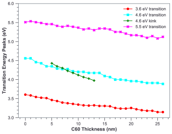
The dynamics of the three electronic transitions of C60 (Figure 1(a)) seem to be different. Initially, the 4.6 eV transition has the highest strength. With addition of C60 (the film grows smoothly, see Section S2) the strength gradually decreases and goes below the 3.6 eV transition as shown in Figure S2, i.e. the rate of decrease of of the 4.6 eV transition (also 5.5 eV) is higher compared to the 3.6 eV transition at least for the initial few nanometers; rate of change of can itself be estimated from the second derivative of Equation 2 but not shown here because of the noisy output of the calculation. Additionally, a kink in the 4.6 eV transition appears at d = 5 nm and persists until 13 nm or approximately a layer of 13 C60 molecules thick/high; the origin of this is not clear. It is possible that some sort of hybridization of the frontier orbitals corresponding to the 4.6 eV transition has occurred leading to its manifestation as a kink. Finally, analysis of the rates of red-shift of the transition peaks is shown in Figure 3. The 4.6 eV transition not only appears to decay faster (along with a kink) but also red-shifts faster (26 meV/nm) compared to the 3.6 eV (18 meV/nm) and the 5.5 eV (15 meV/nm) transitions. The broad, and weak, feature around 2.4 eV (below 3.0 eV), also red-shifting with addition of C60, is visible from the deposition of the first nanometer itself, and corresponds to a forbidden transition which occurs due to mixing of the vibronic states with the forbidden states Leach et al. (1992); Sassara et al. (2001); Lucas et al. (1992); Pavlovich and Shpilevsky (2010); Fukuda and Ehara (2012). Such red-shifts of the transitions with thickness occurring due to coupling is a common feature in organic semiconductors as shown for other systems such as SnPc Gruenewald et al. (2016) and -quaterthiophene Bussetti et al. (2009). Finally, In the energy range corresponding to the transparent region of C60 (from 750 nm or 1.7 eV), any such coupling should be absent, and is reflected in the similar and flat profile of .
Such variation of with thickness shows that the optoelectronic properties of C60 or any such interacting systems is not uniform along the z direction. Moreover, because the wavefunctions of C60 delocalize, the optical response of a layer deposited at time t cannot be solely assigned to that layer Bakulin et al. (2012); Burlingame et al. (2018); Bernardo et al. (2014); Kobayashi et al. (2020). The C60 molecules at the top and bottom of the film will be experiencing different environments, and thus coupling, compared to the molecule in the middle. Hence, the overall could be the sum of all the changes in the underlying bulk layer (of thickness d) along with the layer deposited at time t. This emphasizes that much care is needed when determining the optical constants along the thickness direction from SSE analysis thus highlighting its shortcomings; the values obtained are representative mainly of the properties along the xy or in-plane direction. Thus, the DART method can be used to track the optical properties of vacuum-deposited thin films in real time without the need for real-time model fitting of the iSE data which becomes highly complicated for multli-layered absorbing and anisotropic materials. However, the drawback is that the information obtained will be representative primarily of that of the optical properties in the out-of-plane direction. And to obtain the dielectric constants in interacting systems especially in the out-of-plane direction, as the results show iSE will be insufficient and will need to used in conjunction with other methods such as in-situ DRS Forker et al. (2012) to decouple in-plane and out-of-plane optical properties.
III.3 SubPc
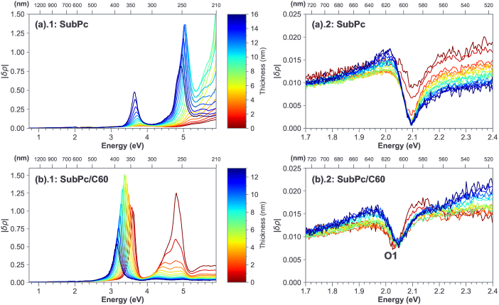
DART analysis of a SubPc film deposited on a silicon wafer is shown in Figure 4(a) (only is shown from here on as it represents n and k together). From the evolution of the data with thickness, we see that a strong electronic coupling between subsequent SubPc layers occurs at energies above 3 eV, i.e. between frontier orbitals lying much higher than for the 2.1 eV * transition Morse and Bender (2012); Rhoda et al. (2016). Figure 4(a).2 is a magnified view of the data in Figure 4(a).1 showing the evolution of the optical response of the * transition (the trough in ) at 2.1 eV in SubPc. From the DART analyses of MeO-TPD and C60, a constant with thickness implies negligible or weak delocalization. Thus, the electronic coupling between frontier orbitals corresponding to the * transition in SubPc appears to occur only until the 3rd or the 4th nanometer after which at 2.1 eV remains constant indicating that the extent of delocalization of this excited state wavefunction is small, i.e. up to a maximum of 4 nm compared to at least 26 nm in C60 (Figure 1). Corresponding SSE analysis of the completed SubPc thin film (16 nm) for the average in-plane and out-of-plane optical constants is shown in Figure S3 (e) and (f). As seen from this figure, an anisotropic model best describes the growth of SubPc (the mean squared error of the fit decreases from 5.4 for an isotropic to 2.1 for an anisotropic model), and a weak transition (O1) at 2 eV can also be seen.
III.4 C60 on phthalocyanines
Intermolecular interactions in the form of electronic coupling between C60 and phthalocyanines were next explored starting with SubPc as the bottom layer. C60 was evaporated onto the completed SubPc film (16 nm) of Figure 4(a) and iSE measurements were carried out during the deposition. The DART analysis is shown in Figure 4(b). Comparing to the growth of C60 on an insulating SiO2 substrate (Figure 1), the data shows strong, anomalous responses centered at 3.6 eV and 4.8 eV (with a shoulder at 4.6 eV). Moreover, with increasing deposition of C60, the response differs from that of C60 on SiO2. The strength of the 3.6 eV transition increases with deposition of C60 until 6 nm, and remains strong, red-shifting and non-zero until the final thickness of 13 nm while that of the 4.8 eV decreases as in the case of C60 on SiO2. Since represents the optical response of the layer that is deposited on the substrate with thin film at thickness d, this implies that at C60 thickness d = 0 nm on top of SubPc, the first incoming C60 molecule interacts (or electronically couples) strongly with SubPc at the 3.6 eV energy corresponding to the primary allowed electronic transition in C60. And as more C60 deposits, a strong overlap and delocalization of the excited state wavefunctions between the incoming C60 and C60 deposited on SubPc is occurring for the frontier orbital corresponding to the 3.6 eV transition. The red-shift of 3.6 eV is more prominent compared to C60 on SiO2. DART analysis of the same data but calculated for a film thickness change of = 1 is shown in Figure S4 highlighting the angstrom-level sensitivity of the method.
Additionally, during deposition of C60 on SubPc, a response can also be seen as a feature near 2.04-2.05 eV shown in the magnified view in Figure 4(b).2, which is not present in the C60 growth on SiO2 in Figure 1 (and Figure S2). Thus, it appears that the origin of this feature is in the underlying SubPc layer. Comparison with the 2.1 eV transition in Figure 4(a).2 shows that this feature is red-shifted from 2.1 eV by about 60 meV, and appears to correspond to the O1 transition in Figure S3(f). The presence of this feature was also investigated by carrying out the DART analysis, calculated for = 1 min, of the iSE data measured during the downtime between the end of SubPc deposition and start of the C60 deposition. The values of the analysis are shown in Figure S5, and are essentially zero indicating that there was no other deposition on the SubPc film during this downtime. The weak, noisy features concentrated around 3.6 eV and 5 eV similar to the energies corresponding to the strong features of SubPc in Figure 4(a).1 suggests a possible mild rearrangement of SubPc molecules (probably on the surface). This observation also suggests that the DART analysis can be used to directly characterize the stability of a film.
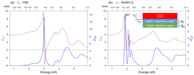
To gain an in-depth understanding of the significance of these anomalous optical responses, systematic analysis of the iSE data was carried out for obtaining the dielectric constants of C60 and the buried SubPc layers using the SSE method. For this, the buried SubPc layer was divided into an interface SubPc layer (ILSubPc) and a bottom SubPc layer (BLSubPc) as shown in the inset in Figure 5(b) (and Figure S6). Subsequently, the iSE data at 12 nm C60 thickness was fit for the out-of-plane dielectric constants ( = nz + jkz of refractive index Nz) of the 12 nm C60 and the ILSubPc layer at thickness = 1 nm shown in Figure 5 (a) and (b) respectively; was fixed at 15 nm with its set to the values before C60 deposition (Figure S3 (e) and (f)). of the layers are fixed since the in-plane environment can be reasonably approximated as unvarying with thickness, i.e. = 0 (see Section S2 for more details on the strategy). In contrast to the values of C60 on SiO2 (Figure 1) and SubPc on SiO2 (Figure S3), the of both C60 and ILSubPc here show significant increase at similar energies found in the DART analysis, i.e. around 3 eV and 2 eV respectively. More importantly, the corresponding real part becomes negative at these values. This holds significant implications. In metal thin films such as Au, Ag and Al, and in conductive oxides such as indium tin oxide, the wavelengths where free electrons absorb are characterized by negative values of with high values due to absorption Fujiwara (2007); Adachi (2012); Lynch and Hunter (1997). The corresponding frequency of light where equals to zero before taking on negative values is called plasma frequency. Hence, observation of such negative values of and a concominant rise in in both C60 and SubPc indicates that strong electronic coupling is occurring between the frontier orbitals corresponding to these specific energies - 3 eV in C60 and 2 eV in SubPc - and is leading to resonance electronic transitions in the form of plasmons (or unbound quasiparticles) oscillating between the molecules, and thus the delocalization of the excited state wavefunctions across the interface. A point to note is that the frontier orbitals corresponding to these excitations are at different energy levels relative to the vacuum level Olthof et al. (2012); Cho et al. (2010); Cnops et al. (2015). The ILSubPc thickness at resonance will be referred to as from here on.
The parameters of the Gaussian oscillators (GO, given by amplitude: Amp, centre energy: En, broadening: Br) representing the two resonance transitions that were fit to the iSE data had good fit statistics, i.e. C60 GO – Amp: 8.3960.693, Br: 0.0760.006, En: 2.9970.003; ILSubPc GO – Amp: 7.5881.361, Br: 0.1120.032, En: 1.8860.024, with a low mean squared error (MSE 4.0) showing high confidence in the derived values. The value of (1 nm) obtained from SSE analysis, i.e. the depth in the SubPc film until which the resonating wavefunctions delocalize, is lower than the 4 nm delocalization distance in SubPc obtained from the DART analysis in Figure 4(a).2. This is probably because of limitations of the SSE method requiring model fitting of a buried layer, and also lack of additional optical information to decouple the optical properties of the top C60 and the buried SubPc layers further highlighting the significance of the DART analysis method. However, can be taken as a lower estimate. Variation of of ILSubPc layer for different values (1-16 nm) is shown in Figure S7, and similarly, variation of of the top C60 layer for its different thicknesses (9-13 nm) is shown in Figure S8, Table S1 for fit statistics of the parameters and Section S2 for more details.
In SubPc, this resonance absorption corresponds not to an increase in the * transition but an increase in its adjacent O1 transition, which was originally observed in the of the bulk film before C60 deposition (see Figure S3(f)). The O1 transition of SubPc at which the strong, plasmonic type coupling occurs with C60 corresponds to excitations into excitonic states. Its energy is below the * transition in SubPc and in accordance with the energies of the SubPc excitons observed from fluorescence emission measurements Morse and Bender (2012); Gommans et al. (2009); Lin et al. (2014). The observed 60 meV Stokes shift in our case, which is about 17 nm shift at 2.1 eV, is in agreement with the 8-30 nm (depending on the environment) observed in boron-subpthalocyanines Ye et al. (2020); Morse and Bender (2012); Kipp et al. (1998); Morse et al. (2010, 2011); Helander et al. (2010). Since the excitons arise from the * transitions – also reflected in the decrease in of the * transitions at 2.1 eV and a concomitant increase in the O1 transition at resonance thickness in Figure S7 – the electronic coupling, and its evolution, of C60 with the electronic wavefunction corresponding to the exciton suggests reorganization of SubPc molecules at the interface with C60. These observations are further corroborated by the DART results of C60 deposited on MoOx/SubPc (SubPcMoOx) and MoOx/hexapropyltruxene (PrT)/SubPc (SubPcPrT) shown in Figures S9 and S10 (SSE analysis for are shown in Figures S7 and S8). The Figures S9(b) and S10(b) show the O1 transition at 2.04 eV and electronic coupling of C60 with SubPc similar to Figure 4 further highlighting the robustness and strength of the DART analysis method. A major difference in the optical response of SubPc deposited on MoOx and PrT with that on SiO2 can also be noticed at energies above 3 eV. We conjecture that this could be due to a possible electronic coupling between SubPc and the underlying electronic materials: MoOx and PrT respectively.
In our previous work Ye et al. (2020) we showed the use of PrT as an interface layer between MoOx and SubPc helping reduce exciton quenching leading to increase in the short-circuit current density (). Such interlayers are regularly used to improve the performance of organic solar cells Yin et al. (2016); Bergemann et al. (2015). SSE analysis in that work also showed the O1 transition in of both SubPcMoOx and SubPcPrT with that of the latter having the highest strength directly corroborating the increased number of excitons in SubPc due to PrT. This increase is also reflected in the increase in value at 3.6 eV upon deposition of C60 on SubPcPrT (Figures S9(b).1 and S10(b).1). With higher number of excitons available in SubPcPrT, higher number of resonance oscillations of the corresponding excited state wavefunctions are occurring with C60 leading to an increased value. This correlation of increased number of excitons leading to an increase in the resonance value is, to an extent, analogous to the observed increase in the absorption at the * interchain transition from regiorandom P3HT to regioregular P3HT Brown et al. (2003); Spano and Silva (2014). The red-shifts of the peak energies of C60 as a function of C60 thickness are shown in Figure S11. The rates of shift are about the same while the peak values for C60/SubPcPrT, C60/SubPcMoOx, C60/SubPcSiO2 (of Figure 4) differ by about 0.1 eV. However, compared to that of C60 on SiO2 (18 meV/nm), the rate of shift is about a factor of 2 higher: 40 meV/nm.
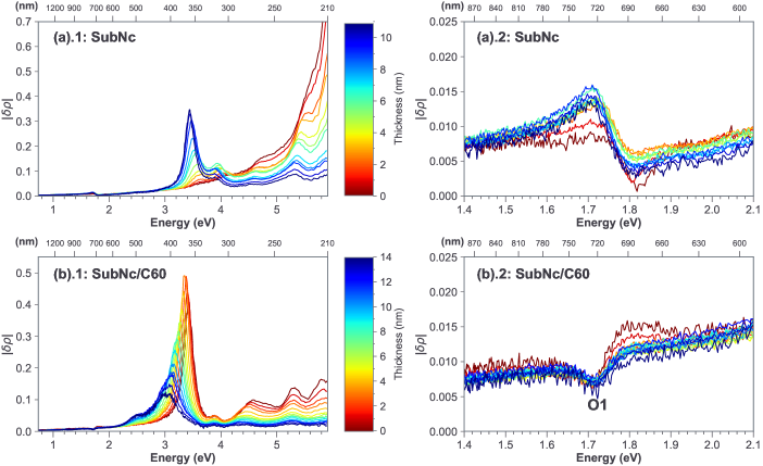
Finally, to ascertain that this type of electronic coupling phenomenon was not specific to SubPc and C60, experiments and data analyses were carried out for SubNc/C60 bilayer. Results similar to SubPc/C60 were observed, and shown in Figures 6 (DART), S7 (SSE: of ILSubNc layer vs ), S8 (SSE: vs C60 thickness), S11 (peak shifts) and Table S1 (fit statistics of the O1 transition). Figure 6(a) shows, as for SubPc, firstly, strong electronic coupling, and delocalization, occurring between frontier orbitals of SubNc (deposited on silicon wafer with 4 nm MoOx) at energies above 3 eV. For the wavefunction corresponding to the * transition, the delocalization distance is about 2-3 nm after which remains approximately constant. Figure 6(b) shows the same type of coupling as for SubPc/C60 between the wavefunction corresponding to SubNc exciton (O1) and that of the 3.6 eV primary transition in C60, along with delocalization, further corroborating the results.
The plasmonic type absorption () at very specific energies occurring upon deposition of C60 on the phthalocyanines implies resonance oscillations of the excited state wavefunctions between the two materials across the interface. The question of specificity in energies of the frontier orbitals at which electronic coupling is occurring can be partly investigated by examining the transitions in pure C60. The lower energy HOMOLUMO transitions are forbidden in C60 since the states are of the same parity. The primary electronic transitions are (or HOMOLUMO+1) and approximately centered around 3.6 eV, 4.6 eV and 5.5 eV Leach et al. (1992); Lucas et al. (1992); Pavlovich and Shpilevsky (2010); Fukuda and Ehara (2012); Orlandi and Negri (2002); Montero-Alejo et al. (2012); Bauernschmitt et al. (1998), and are also the wavefunctions which spatially delocalize between C60 molecules as seen in Figures 1, 4, 6, S9 and S10. From our observations, it appears that the physics dictating the transitions within C60, i.e. Fermi’s golden rule Köhler and Bassler (2015); Pope and Swenberg (1999); Dirac and Bohr (1927), also seems to dictate the transitions from other molecules – arising from resonance oscillations – into C60. More specifically, the question of why electronic coupling is occurring at 3.6 eV and not the other primary transitions is difficult to answer at this point. We can only conjecture which is that the frontier orbitals corresponding to the 3.6 eV primary transition is closest in energy, relative to the vacuum level, to that of the * transition in the phthalocyanines. This coupling might have consequences for exciton dissociation from phthalocyanine to C60 and vice versa. In light of these intriguing observations, understanding their implications in the perspective of quantum mechanics and solar cell device physics is of pivotal importance, and will be explored in our next work with further donors and acceptors including non-fullerene acceptors, and at different substrate temperatures to explore the effects of molecular orientation on electronic coupling. The method will also be applied to test for Fermi-level pinning arising due to electronic coupling between organic semiconductors and metal electrodes.
IV CONCLUSIONS
We have shown a novel method for analysing in-situ spectroscopic ellipsometry data yielding direct information representative of the optical properties (dielectric constants) primarily along the growth direction of vacuum-deposited thin films in real time without the need for model fitting. Application of this analysis method to the study of pristine organic semiconductor thin films, C60 and MeO-TPD on SiO2, showed electronic coupling and delocalization of the excited state wavefunctions corresponding to the frontier orbitals. Extending the same to the growth of C60 on phthalocyanines (SubPc and SubNc), strong, anomalous optical features were observed in C60 at energies corresponding to its primary allowed transition at 3.6 eV, which increased and then decreased in strength while red-shifting with C60 deposition. Accompanying features were observed in the underlying phthalocyanine layers at energies corresponding to their excitons. Dielectric constants along the growth or thickness direction of the bilayer films derived from systematic analysis using standard ellipsometry data analysis method (model fitting) revealed such features to be plasmonic type oscillations of the excited state wavefunctions corresponding to phthalocyanine excitons and the 3.6 eV primary transition of C60, the strength of which changed with the number of excitons. Spatial delocalization (along the thickness direction) of the wavefunctions in C60 and phthalocyanines was also observed.
These results using the new analysis method have revealed singular insights into the physics of fullerene C60 and phthalocyanines in the thickness direction, and thus understanding the implications on organic optoelectronics device physics such as organic solar cells will be crucial. In the case of deposition techniques where in-situ growth measurements are not possible such as solution-processing methods, the DART method can still be used to study post-treatment effects, e.g. DART analysis could give insights into effects of structural changes on the optical properties, for example, from thermal treatment, and consequently structure-property relationships and stability can be examined. And finally, strength of the presented analysis method as displayed in its simplicity, angstrom-level sensitivity, robustness and reproducibility, could be highly useful in conjunction with other in-situ optical spectroscopy methods Forker et al. (2012); Martin and Weightman (2004) in examining thin film systems comprising of semiconductors, quantum materials or any other materials where interfacial electronic coupling is highly crucial in determining the device properties.
SUPPLEMENTARY MATERIAL
See the supplementary material for a basic derivation of ; standard spectroscopic ellipsometry (SSE) analysis description and issues; derived dielectric constants; fit statistics of the O1 transition parameters; DART results of C60 on SiO2, time gap between SubPc and C60, C60 on SiO2/SubPc calculated for = 1 , C60 on MoOx/SubPc and PrT/SubPc; and peak energy values of C60 vs C60 thickness deposited on the different SubPc films and SubNc film.
ACKNOWLEDGEMENTS
SVK would like to thank the AFMD group, headed by MKR at Oxford, especially Anna Jungbluth, Andreas E. Lauritzen, Dr. Alberto Privitera, Irfan Habib, Dr. Pascal Kaienburg, Dr. Thomas Derrien for the valuable discussions and feedback on the manuscript. SVK and MKR would also like to thank Prof. Peter Skabara, School of Chemistry, University of Glasgow for hexapropyltruxene. SVK expresses gratitude to EPSRC (WAFT, Grant No. EP/M015173/1; IAA, Grant No. EP/R511742/1) and UKRI (START, Grant No. ST/R002754/1) for funding. The research materials (iSE data) supporting this publication can be publicly accessed on the Oxford University Research Archive via the following digital object identifier: https://doi.org/10.5287/bodleian:KzjB5BnPb. The research materials are available under a CC BY license.
AUTHOR CONTRIBUTIONS
SVK developed the DART method, and conceptualized and executed the study. Discussion of the results and planning the experiments were carried out by SVK and MKR. The first draft was written by SVK. All authors participated in the preparation and review.
ORCID iD
SVK: 0000-0001-5526-0780
MKR: 0000-0002-5399-5510
COMPETING INTERESTS
Oxford University Innovation has filed a UK patent application related to the DART method of this manuscript. Application No.: 2002576.3, Status: Pending.
References
- Ashcroft and Mermin (1976) Neil W Ashcroft and N David Mermin, Solid state physics (Brooks/Cole, Thomson Learning, South Melbourne ; London, 1976).
- Simon (2013) Steven H. Simon, The Oxford solid state basics (Oxford University Press, Oxford, 2013).
- Azzouzi et al. (2018) Mohammed Azzouzi, Jun Yan, Thomas Kirchartz, Kaikai Liu, Jinliang Wang, Hongbin Wu, and Jenny Nelson, “Nonradiative Energy Losses in Bulk-Heterojunction Organic Photovoltaics,” Physical Review X 8, 31055 (2018).
- Eisner et al. (2019) Flurin D Eisner, Mohammed Azzouzi, Zhuping Fei, Xueyan Hou, Thomas D Anthopoulos, T John S Dennis, Martin Heeney, and Jenny Nelson, “Hybridization of Local Exciton and Charge-Transfer States Reduces Nonradiative Voltage Losses in Organic Solar Cells,” Journal of the American Chemical Society 141, 6362–6374 (2019).
- Athanasopoulos et al. (2019) Stavros Athanasopoulos, Heinz Bässler, and Anna Köhler, “Disorder vs Delocalization: Which Is More Advantageous for High-Efficiency Organic Solar Cells?” The Journal of Physical Chemistry Letters 10, 7107–7112 (2019).
- Kahle et al. (2018) Frank-Julian Kahle, Christina Saller, Selina Olthof, Cheng Li, Jenny Lebert, Sebastian Weiß, Eva M Herzig, Sven Hüttner, Klaus Meerholz, Peter Strohriegl, and Anna Köhler, “Does Electron Delocalization Influence Charge Separation at Donor–Acceptor Interfaces in Organic Photovoltaic Cells?” The Journal of Physical Chemistry C 122, 21792–21802 (2018).
- Menke et al. (2018) S Matthew Menke, Niva A Ran, Guillermo C Bazan, and Richard H Friend, “Understanding Energy Loss in Organic Solar Cells: Toward a New Efficiency Regime,” Joule 2, 25–35 (2018).
- Gélinas et al. (2014) Simon Gélinas, Akshay Rao, Abhishek Kumar, Samuel L Smith, Alex W Chin, Jenny Clark, Tom S Van Der Poll, Guillermo C Bazan, and Richard H Friend, “Ultrafast Long-Range Charge Separation in Organic Semiconductor Photovoltaic Diodes,” 343, 512–517 (2014).
- Forker et al. (2012) Roman Forker, Marco Gruenewald, and Torsten Fritz, “Optical differential reflectance spectroscopy on thin molecular films,” Annual Reports Section "C" (Physical Chemistry) 108, 34–68 (2012).
- Gruenewald et al. (2016) Marco Gruenewald, Julia Peuker, Matthias Meissner, Falko Sojka, Roman Forker, and Torsten Fritz, “Impact of a molecular wetting layer on the structural and optical properties of tin(II)-phthalocyanine multilayers on Ag(111),” Physical Review B 93, 115418 (2016).
- Aspnes and Studna (1985) D. E. Aspnes and A. A. Studna, “Anisotropies in the above—band-gap optical spectra of cubic semiconductors,” Phys. Rev. Lett. 54, 1956–1959 (1985).
- Martin and Weightman (2004) D.S. Martin and P. Weightman, “Reflection anisotropy spectroscopy of molecular assembly at metal surfaces,” Thin Solid Films 455-456, 752 – 758 (2004), the 3rd International Conference on Spectroscopic Ellipsometry.
- Bussetti et al. (2009) G. Bussetti, S. Cirilli, A. Violante, V. Chiostri, C. Goletti, P. Chiaradia, A. Sassella, M. Campione, L. Raimondo, D. Braga, and A. Borghesi, “Reflectance anisotropy spectroscopy: A probe to explore organic epitaxial growth,” Journal of Vacuum Science & Technology A 27, 1029–1034 (2009).
- Fujiwara (2007) Hiroyuki Fujiwara, Spectroscopic ellipsometry : principles and applications (John Wiley, Chichester, 2007).
- Azzam and Bashara (1977) R.M.A Azzam and N.M Bashara, Ellipsometry and polarized light (Amsterdam; Oxford : North-Holland, Amsterdam, NY, 1977).
- Hinrichs et al. (2012) Karsten Hinrichs, Marieta Levichkova, David Wynands, Karsten Walzer, Klaus J. Eichhorn, Peter Bäuerle, Karl Leo, and Moritz Riede, “Morphology and molecular orientation of ethyl-substituted dicyanovinyl-sexithiophene films for photovoltaic applications,” Thin Solid Films 525, 97 – 105 (2012).
- Yokoyama (2011) Daisuke Yokoyama, “Molecular orientation in small-molecule organic light-emitting diodes,” Journal of Materials Chemistry 21, 19187–19202 (2011).
- Klein et al. (2015) Michael F. G. Klein, Gustavo Q. Glasner de Medeiros, Panagiota Kapetana, Uli Lemmer, and Alexander Colsmann, “Modeling approach to derive the anisotropic complex refractive index of polymer:fullerene blends for organic solar cells utilizing spectroscopic ellipsometry,” Journal of Photonics for Energy 5, 1–16 (2015).
- Schünemann et al. (2013) Christoph Schünemann, David Wynands, Klaus-Jochen Eichhorn, Manfred Stamm, Karl Leo, and Moritz Riede, “Evaluation and control of the orientation of small molecules for strongly absorbing organic thin films,” The Journal of Physical Chemistry C 117, 11600–11609 (2013).
- Burkhard et al. (2010) George F. Burkhard, Eric T. Hoke, and Michael D. McGehee, “Accounting for interference, scattering, and electrode absorption to make accurate internal quantum efficiency measurements in organic and other thin solar cells,” Advanced Materials 22, 3293–3297 (2010).
- Yokoyama and Adachi (2010) Daisuke Yokoyama and Chihaya Adachi, “In situ real-time spectroscopic ellipsometry measurement for the investigation of molecular orientation in organic amorphous multilayer structures,” Journal of Applied Physics 107, 123512 (2010).
- Ye et al. (2020) Hanyang Ye, Sameer Vajjala Kesava, Josué F. Martínez Hardigree, Roisin E. Brown, Giulio Mazzotta, Ross Warren, Peter J. Skabara, and Moritz Riede, “Efficiency enhancement of small molecule organic solar cells using hexapropyltruxene as an interface layer,” Journal of Materials Chemistry C 8, 4909–4918 (2020).
- Heitz and Drévillon (1998) T Heitz and B Drévillon, “In situ infrared ellipsometry study of the growth of hydrogenated amorphous carbon thin films,” Thin Solid Films 313-314, 704–707 (1998).
- Leach et al. (1992) Sydney Leach, Michel Vervloet, Alain Desprès, Emilienne Bréheret, Jonathan P. Hare, T. John Dennis, Harold W. Kroto, Roger Taylor, and David R.M. Walton, “Electronic spectra and transitions of the fullerene c60,” Chemical Physics 160, 451 – 466 (1992).
- Sassara et al. (2001) Andrea Sassara, Gerald Zerza, Majed Chergui, and Sydney Leach, “Absorption wavelengths and bandwidths for interstellar searches of c 60 in the 2400–4100 a region,” The Astrophysical Journal Supplement Series 135, 263–273 (2001).
- Lucas et al. (1992) A Lucas, G Gensterblum, JJ Pireaux, PA Thiry, R Caudano, JP Vigneron, P Lambin, and W Krätschmer, “Elementary excitations of c60 from the far infrared to the far vacuum ultraviolet studied by high-resolution electron-energy-loss spectroscopy,” Physical Review B 45, 13694—13702 (1992).
- Pavlovich and Shpilevsky (2010) V S Pavlovich and E M Shpilevsky, “Absorption and fluorescence spectra of c60 fullerene concentrated solutions in hexane and polystyrene at 77–300 k,” Journal of Applied Spectroscopy 77, 335–342 (2010).
- Fukuda and Ehara (2012) Ryoichi Fukuda and Masahiro Ehara, “Electronic excitations of c60 fullerene calculated using the ab initio cluster expansion method,” The Journal of Chemical Physics 137, 134304 (2012).
- Bakulin et al. (2012) Artem A. Bakulin, Akshay Rao, Vlad G. Pavelyev, Paul H. M. van Loosdrecht, Maxim S. Pshenichnikov, Dorota Niedzialek, Jérôme Cornil, David Beljonne, and Richard H. Friend, “The role of driving energy and delocalized states for charge separation in organic semiconductors,” Science 335, 1340–1344 (2012).
- Burlingame et al. (2018) Quinn Burlingame, Caleb Coburn, Xiaozhou Che, Anurag Panda, Yue Qu, and Stephen R. Forrest, “Centimetre-scale electron diffusion in photoactive organic heterostructures,” Nature 554, 77–80 (2018).
- Bernardo et al. (2014) B Bernardo, D Cheyns, B Verreet, R D Schaller, B P Rand, and N C Giebink, “Delocalization and dielectric screening of charge transfer states in organic photovoltaic cells,” Nature Communications 5, 3245 (2014).
- Kobayashi et al. (2020) Hajime Kobayashi, Shinnosuke Hattori, Raku Shirasawa, and Shigetaka Tomiya, “Wannier-like delocalized exciton generation in c60 fullerene clusters: A density functional theory study,” The Journal of Physical Chemistry C 124, 2379–2387 (2020).
- Jelley (1936) Edwin E. Jelley, “Spectral Absorption and Fluorescence of Dyes in the Molecular State,” Nature 138, 1009–1010 (1936).
- Scheibe (1937) G Scheibe, “Über die veränderlichkeit der absorptionsspektren in lösungen und die nebenvalenzen als ihre ursache,” Angewandte Chemie 50, 212–219 (1937).
- Köhler and Bassler (2015) Anna Köhler and Heinz Bassler, Electronic Processes in Organic Semiconductors (Wiley-VCH, Weinheim, 2015).
- Pope and Swenberg (1999) Martin Pope and C. E. Swenberg, Electronic Processes of Organic Crystals and Polymers (Clarendon Press, Oxford, 1999).
- Tietze et al. (2012) Max L Tietze, Lorenzo Burtone, Moritz Riede, Björn Lüssem, and Karl Leo, “Fermi level shift and doping efficiency in p-doped small molecule organic semiconductors: A photoelectron spectroscopy and theoretical study,” Physical Review B 86, 35320 (2012).
- Meerheim et al. (2011) Rico Meerheim, Selina Olthof, Martin Hermenau, Sebastian Scholz, Annette Petrich, Nir Tessler, Olga Solomeshch, Björn Lüssem, Moritz Riede, and Karl Leo, “Investigation of c60f36 as low-volatility p-dopant in organic optoelectronic devices,” Journal of Applied Physics 109, 103102 (2011).
- Olthof et al. (2012) Selina Olthof, Ronny Timmreck, Moritz Riede, and Karl Leo, “Photoelectron spectroscopy investigations of recombination contacts for tandem organic solar cells,” Applied Physics Letters 100, 113302 (2012).
- Morse and Bender (2012) Graham E. Morse and Timothy P. Bender, “Boron subphthalocyanines as organic electronic materials,” ACS Applied Materials & Interfaces 4, 5055–5068 (2012).
- Rhoda et al. (2016) Hannah M. Rhoda, Mathew P. Kayser, Yefeng Wang, Alexander Y. Nazarenko, Rodion V. Belosludov, Paul Kiprof, David A. Blank, and Victor N. Nemykin, “Tuning up an electronic structure of the subphthalocyanine derivatives toward electron-transfer process in noncovalent complexes with c60 and c70 fullerenes: Experimental and theoretical studies,” Inorganic Chemistry 55, 9549–9563 (2016).
- Adachi (2012) Sadao Adachi, The Handbook on Optical Constants of Metals (World Scientifc, 2012).
- Lynch and Hunter (1997) David W Lynch and W R Hunter, “Comments on the Optical Constants of Metals and an Introduction to the Data for Several Metals,” in Handbook of Optical Constants of Solids, edited by Edward D Palik (Academic Press, Burlington, 1997) pp. 275–367.
- Cho et al. (2010) S W Cho, L F J Piper, A DeMasi, A R H Preston, K E Smith, K V Chauhan, P Sullivan, R A Hatton, and T S Jones, “Electronic Structure of C60/Phthalocyanine/ITO Interfaces Studied using Soft X-ray Spectroscopies,” The Journal of Physical Chemistry C 114, 1928–1933 (2010).
- Cnops et al. (2015) Kjell Cnops, German Zango, Jan Genoe, Paul Heremans, M Victoria Martinez-Diaz, Tomas Torres, and David Cheyns, “Energy Level Tuning of Non-Fullerene Acceptors in Organic Solar Cells,” Journal of the American Chemical Society 137, 8991–8997 (2015).
- Gommans et al. (2009) H. Gommans, S. Schols, A. Kadashchuk, P. Heremans, and S. C. J. Meskers, “Exciton diffusion length and lifetime in subphthalocyanine films,” The Journal of Physical Chemistry C 113, 2974–2979 (2009).
- Lin et al. (2014) Chi-Feng Lin, Valerie M Nichols, Yung-Chih Cheng, Christopher J Bardeen, Mau-Kuo Wei, Shun-Wei Liu, Chih-Chien Lee, Wei-Cheng Su, Tien-Lung Chiu, Hsieh-Cheng Han, Li-Chyong Chen, Chin-Ti Chen, and Jiun-Haw Lee, “Chloroboron subphthalocyanine/C60 planar heterojunction organic solar cell with N,N-dicarbazolyl-3,5-benzene blocking layer,” Solar Energy Materials and Solar Cells 122, 264–270 (2014).
- Kipp et al. (1998) Rachael A Kipp, Jerald A Simon, Matthew Beggs, Harry E Ensley, and Russell H Schmehl, “Photophysical and Photochemical Investigation of a Dodecafluorosubphthalocyanine Derivative,” The Journal of Physical Chemistry A 102, 5659–5664 (1998).
- Morse et al. (2010) Graham E Morse, Michael G Helander, Jozef F Maka, Zheng-Hong Lu, and Timothy P Bender, “Fluorinated Phenoxy Boron Subphthalocyanines in Organic Light-Emitting Diodes,” ACS Applied Materials & Interfaces 2, 1934–1944 (2010).
- Morse et al. (2011) Graham E Morse, Jeffery S Castrucci, Michael G Helander, Zheng-Hong Lu, and Timothy P Bender, “Phthalimido-boronsubphthalocyanines: New Derivatives of Boronsubphthalocyanine with Bipolar Electrochemistry and Functionality in OLEDs.” ACS Applied Materials & Interfaces 3, 3538–3544 (2011).
- Helander et al. (2010) Michael G Helander, Graham E Morse, Jacky Qiu, Jeffrey S Castrucci, Timothy P Bender, and Zheng-Hong Lu, “Pentafluorophenoxy Boron Subphthalocyanine As a Fluorescent Dopant Emitter in Organic Light Emitting Diodes,” ACS Applied Materials & Interfaces 2, 3147–3152 (2010).
- Yin et al. (2016) Zhigang Yin, Jiajun Wei, and Qingdong Zheng, “Interfacial Materials for Organic Solar Cells: Recent Advances and Perspectives,” Advanced Science 3, 1500362 (2016).
- Bergemann et al. (2015) Kevin J Bergemann, Jojo A Amonoo, Byeongseop Song, Peter F Green, and Stephen R Forrest, “Surprisingly High Conductivity and Efficient Exciton Blocking in Fullerene/Wide-Energy-Gap Small Molecule Mixtures,” Nano Letters 15, 3994–3999 (2015).
- Brown et al. (2003) Peter J Brown, D Steve Thomas, Anna Köhler, Joanne S Wilson, Ji-Seon Kim, Catherine M Ramsdale, Henning Sirringhaus, and Richard H Friend, “Effect of interchain interactions on the absorption and emission of poly(3-hexylthiophene),” Physical Review B 67, 64203 (2003).
- Spano and Silva (2014) Frank C Spano and Carlos Silva, “H- and J-Aggregate Behavior in Polymeric Semiconductors,” Annual Review of Physical Chemistry 65, 477–500 (2014).
- Orlandi and Negri (2002) Giorgio Orlandi and Fabrizia Negri, “Electronic states and transitions in C60 and C70 fullerenes,” Photochemical & Photobiological Sciences 1, 289–308 (2002).
- Montero-Alejo et al. (2012) A L Montero-Alejo, E Menendez-Proupin, M E Fuentes, A Delgado, F.-P. Montforts, L A Montero-Cabrera, and J M Garcia de la Vega, “Electronic excitations of C60 aggregates,” Physical Chemistry Chemical Physics 14, 13058–13066 (2012).
- Bauernschmitt et al. (1998) Rüdiger Bauernschmitt, Reinhart Ahlrichs, Frank H Hennrich, and Manfred M Kappes, “Experiment versus Time Dependent Density Functional Theory Prediction of Fullerene Electronic Absorption,” Journal of the American Chemical Society 120, 5052–5059 (1998).
- Dirac and Bohr (1927) Paul Adrien Maurice Dirac and Niels Henrik David Bohr, “The quantum theory of the emission and absorption of radiation,” Proceedings of the Royal Society of London. Series A, Containing Papers of a Mathematical and Physical Character 114, 243–265 (1927).