Spatially Resolved Persistent Photoconductivity in MoS2–WS2 Lateral Heterostructures
Abstract
The optical and electronic properties of 2D semiconductors are intrinsically linked via the strong interactions between optically excited bound species and free carriers. Here we use near-field scanning microwave microscopy (SMM) to image spatial variations in photoconductivity in MoS2–WS2 lateral multijunction heterostructures using photon energy-resolved narrowband illumination. We find that the onset of photoconductivity in individual domains corresponds to the optical absorption onset, confirming that the tightly bound excitons in transition metal dichalcogenides can nonetheless dissociate into free carriers. These photogenerated carriers are most likely n-type and are seen to persist for up to days, and informed by finite element modeling we reveal that they can increase the carrier density by up to 200 times. This persistent photoconductivity appears to be dominated by contributions from the multilayer MoS2 domains, and we attribute the flake-wide response in part to charge transfer across the heterointerface. Spatial correlation of our SMM imaging with photoluminescence (PL) mapping confirms the strong link between PL peak emission photon energy, PL intensity, and the local accumulated charge. This work reveals the spatially and temporally complex optoelectronic response of these systems and cautions that properties measured during or after illumination may not reflect the true dark state of these materials but rather a metastable charged state.
NIST Boulder] Applied Physics Division, National Institute of Standards and Technology, Boulder, CO NREL] Materials and Chemical Science and Technology Directorate, National Renewable Energy Laboratory, Golden, CO USF] Department of Physics, University of South Florida, Tampa, FL \alsoaffiliation[IIT] Materials Science Centre, Indian Institute of Technology Kharagpur, India Penn State] The Pennsylvania State University, State College, PA \alsoaffiliation[NIST Boulder] Applied Physics Division, National Institute of Standards and Technology, Boulder, CO NREL] Materials and Chemical Science and Technology Directorate, National Renewable Energy Laboratory, Golden, CO NREL] Materials and Chemical Science and Technology Directorate, National Renewable Energy Laboratory, Golden, CO NIST Boulder] Applied Physics Division, National Institute of Standards and Technology, Boulder, CO USF] Department of Physics, University of South Florida, Tampa, FL NIST Boulder] Applied Physics Division, National Institute of Standards and Technology, Boulder, CO NREL] Materials and Chemical Science and Technology Directorate, National Renewable Energy Laboratory, Golden, CO
While the properties of two-dimensional semiconductors typically mirror those of their bulk counterparts, their properties are augmented by effects arising from their reduced dimensionality 1, 2, the lattice symmetry 3, and enhanced interactions with the environment. For instance, the strong many-body interactions resulting from the quantum confinement give rise to excitons and other bound species 4, 5 whose binding energies significantly exceed the thermal energy at room temperature and are thus stable under ambient conditions. The interaction energies of these bound excited species 6, 4, their optical transition dipole moments, and the competition between radiative and nonradiative decay are strongly affected by the presence of free charge carriers 7 and neutral bound species, as well as environmental influences such as surface adsorbates 8, 9 or chemical treatments 10, 11. The influence of free carriers on the optical properties are particularly strong since they underpin the competition between neutral excitons (X0) and carrier-bound excitons (trions, X- and X+) 5, 4 and can drastically affect the photoluminescence quantum efficiency 7. The optical and electronic properties of these materials are thus inextricably linked, and disentangling the two has remained challenging 12 in large part due to spatial inhomogeneities that occur on nanometer scales and large variations in sample properties due to processing and growth.
A comprehensive understanding of the optoelectronic properties therefore requires spatially resolved characterization of both the electronic and optical properties to address their interplay and the influence of spatial inhomogeneities. Optical microscopy can readily obtain diffraction-limited spatial resolution of several 100s of nanometers and near-field implementations can achieve resolution as high as 10s of nanometers 13, 14, 15. Unfortunately, in addition to indirectly modifying electrical characteristics through local heating, optical absorption leads to excited states that can produce long-term photodoping in MoS2 16, 17 that can persist for days 18. Directly measuring the electronic properties of 2D materials by device transport is routine 19, 20, though this only yields device-average properties. Spatially resolved electronic information is typically obtained using atomic force microscope (AFM)-based characterization such as Kelvin probe force microscopy (KPFM). KPFM can quantify the local work function 20, 21 and can be used to estimate carrier densities in functional devices 22, but it does not directly measure the free carrier density and requires electrically contacted samples.
In this work, we perform a correlated study of the local electronic, optoelectronic, and optical properties of transition metal dichalcogenide (TMD) lateral heterostructures consisting of MoS2–WS2 multijunctions. The nanoelectronic characterization is performed using near-field scanning microwave microscopy (SMM, also called scanning microwave impedance microscopy, sMIM). SMM interacts directly with the local intrinsic as well as photoexcited 23, 24, 25 free carriers in a sample and can characterize electrically isolated structures placed on insulating substrates with spatial resolution limited only by the tip apex radius. This work is enabled by a spectrally narrow ( 10 nm bandwidth) continuously tunable optical excitation source that we combine with SMM to study the photon energy-dependent spatial distribution of photogenerated carriers as well as their long-term behavior. We find good correspondence between the photon energy at which photoconductivity emerges in the individual domains, and the expected absorption onset, which confirms that excitons can readily dissociate into free carriers despite their large binding energies. The optoelectronic response is dominated by photoinduced n-type charging that is most pronounced in the multilayer MoS2 regions and can lead to a localized increase in carrier density by up to a factor of 200. This persistent photoconductivity also leads to uniform n-type conductivity throughout all domains of the flake which we attribute in part to charge transfer across the heterointerface. Using spatially correlated photoluminescence (PL) microscopy mapping, we further show a clear correspondence between the persistent photoconductivity and the interplay of X0- and X--emission that arises from the presence of free carriers.
Results
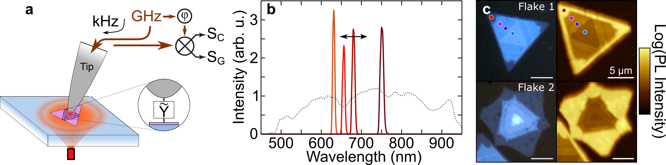
Shown in Figure 1a is a schematic of the experimental setup. The SMM is based on a heavily modified AFM (Keysight / Agilent*) operating in contact mode 26. SMM is directly sensitive to changes in sample conductivity via its effect on the complex-valued tip-sample admittance , with the conductance , capacitance , and frequency . Phase-resolved detection of the microwave signal is used to separate the real and imaginary terms, and , respectively. Differential measurements 26 are performed by applying an AC tip bias with peak-to-peak amplitude = 1 V at a frequency = 50 kHz. Lock-in demodulation on at then yields the differential signals and .
For SMM photoconductivity mapping, we use spectral amplitude shaping to generate a continuously tunable optical excitation source with 10 nm spectral bandwidth from a broadband supercontinuum laser (Fianium Ltd*). Shown in Figure 1b are representative narrowband excitation spectra at 630, 655, 680 and 750 nm (1.97, 1.89, 1.82, and 1.65 eV, respectively), as well as the full source supercontinuum spectrum (dashed line, not to scale). Unless otherwise noted, all images are acquired under illumination at the photon energy indicated.
The samples were also characterized using a micro-photoluminescence (PL) setup operating under ambient conditions using an excitation wavelength of 532 nm (2.38 eV). Shown in Figure 1c are contrast-enhanced optical images of the two flakes studied in this work (left, see supporting information for original images and contrast-optimized ones) as well as the corresponding spatially resolved log-scale photoluminescence (PL) maps (right) showing the maximum emission intensity at each spatial pixel. These flakes will be referred to as flake 1 and flake 2 throughout the remaining text. The control of single layer (SL) 27 and bilayer (BL) 28 growth using our one-pot method is established, and a comparison with extensively characterized as-grown flakes (see supporting information) confirms that the outer regions with weak optical contrast but strong PL emission are SL, while the interior multilayer (ML) regions with stronger optical contrast and weak PL emission are BL with the exception of thicker regions at the center of flake 2.
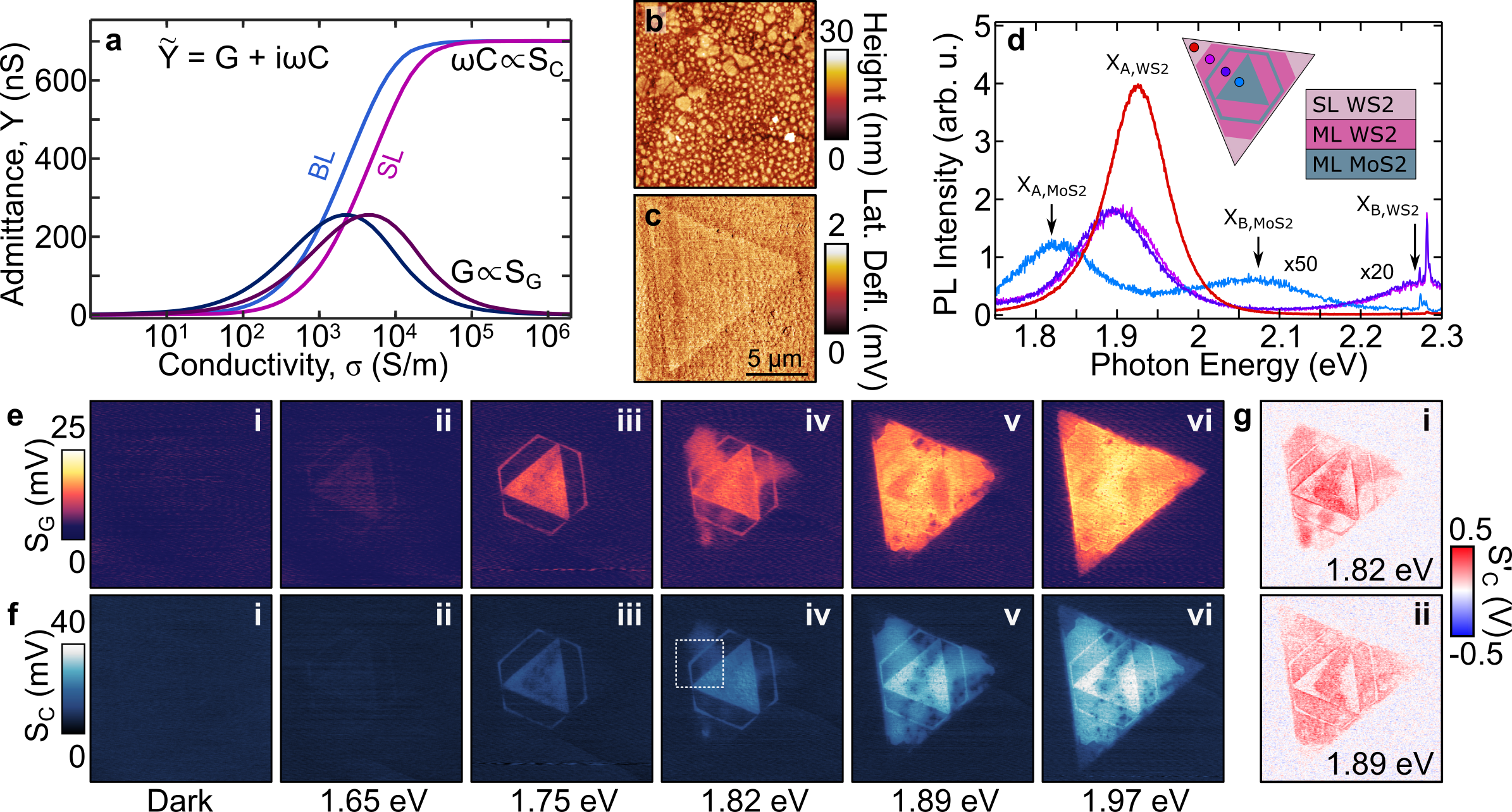
SMM is directly sensitive to the local carrier density via the sample conductivity = with the elementary charge and the corresponding mobility and carrier density, and , respectively ( = , ). Shown in Figure 2a is the finite-element simulated complex-valued tip-sample admittance = at our chosen frequency of 17.2 GHz as a function of conductivity for SL and BL flakes as indicated. For few-layer 2D materials, the admittance depends on the sheet resistance, a function of the layer thickness. As the film thickness changes, the admittance curve is thus moved to higher (thinner) or lower (thicker) conductivity values. Importantly, the capacitive signal (SC) increases monotonically with sample conductivity, providing a qualitative measure of its spatial distribution.
Shown in Figure 2b is the contact-mode AFM topography of flake 1. Although the AFM used can readily resolve SL flakes 29, the flake is obscured by substrate roughness. The location of the flake is clearly seen in the lateral deflection signal shown in Figure 2c, which arises from differences in friction as the tip is pulled across the sample. The different domains of the heterostructure are schematically shown in the inset of Figure 2d. As confirmed by the lack of streaking artifacts in the AFM topography and lateral deflection, we ensure that the samples are free of polymer residue by repeated scanning.
Shown in Figure 2d are PL spectra of the flakes acquired from the corresponding positions marked in Figure 1c and the inset, which schematically shows the different regions of flake 1. MoS2 and WS2 have SL optical bandgaps of 1.8 and 2.0 eV 1, 30 with the absorption blue-shifted relative to the PL by a few 10s of meV 31. The strongest emission seen in Figure 1c originates from the direct bandgap A-exciton (XA) emission of the SL domain of WS2 30 present on the outside of most flakes on this sample. In contrast, the significantly diminished PL intensity in the interior of the flakes originates from ML domains of WS2 and MoS2 whose PL spectra show both XA and B-exciton (XB) emission 31, 30. Although the spectral resolution is optimized to measure the broad PL emission, the stokes-shifted Raman emission 32 is also seen at the position of the WS2 XB emission in Figure 2d. We note that although the ML domains all show weak PL emission, the ML WS2 shows consistently stronger emission compared to the ML MoS2.
In Figure 2e and f we show the evolution of the SG and topographically corrected 33 (see supporting information) SC microwave near-field images in chronological order from left to right as the illumination is turned on and the photon energy increased. Under dark conditions the conductivity in all domains of the flake is below the instrument sensitivity limit with no discernible contrast. As discussed in detail below, charging and residual free carriers are seen for up to 72 hours in these flakes after illumination; therefore the data shown in Figure 2ei and fi was obtained after 4 days of illumination-free conditions to ensure that no photo-residual effects were measured.
While no discernible conductivity is seen in the uncharged dark state, after illumination of the flake with 1.65 eV excitation, weak photoconductivity emerges in the MoS2 domains. As the photon energy is increased to 1.75 eV and approaches the XA transition 31, the photoconductivity in the MoS2 domain increases. Upon excitation at the approximate XA transition energy at 1.82 eV, the photoconductivity in the MoS2 domain further increases and a discernible conductivity is also seen over portions of the ML WS2 domain. At 1.89 eV the conductivity over the whole flake is seen to increase and a weak contrast emerges at the SL WS2 vertices of the flake. Lastly, at a photon energy approximately corresponding to the WS2 XA transition at 1.97 eV, all domains of the flake show discernible photoconductivity, including the SL WS2 at the vertices and outer edges, though the higher contrast in the SC channel suggests that the MoS2 domains remain the most conductive. Of particular note are spatially localized regions of reduced photoconductivity visible throughout the flake. A careful comparison with the substrate topography suggests that these are not related to topographically-induced strain, though many appear to originate from dark regions in the optical images of Figure 1c (see supporting information for contrast-optimized images).
As differential measurements are directly sensitive to the local carrier type via the phase of the lock-in response 26, they directly identify local variations in the carrier type and provide complementary information to the conductivity images. Shown in Figure 2g are S images acquired at photon energies of 1.82 eV and 1.89 eV. The sign of the lock-in signal remains positive throughout the flake, indicating that the conductivity is dominated by the same charge carrier type in both materials. Understanding the observed photoconductive response of these flakes thus requires a detailed examination of the persistent photoconductivity as well as the effects of the interface.
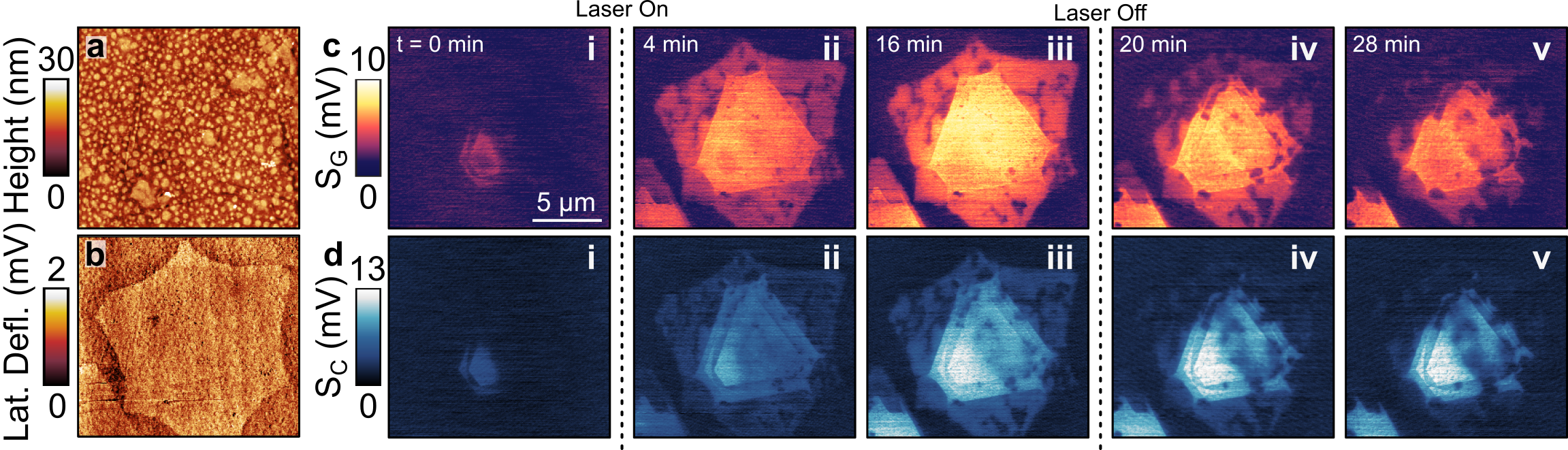
We now turn to the dynamics of photogenerated charge carriers in these materials. As noted above, long-term charging is observed in these flakes, with residual photoconductivity that is seen to persist for days. Shown in Figure 3a and b are the AFM topography and lateral deflection signal of flake 2. Shown in Figure 3c and d are select SG and SC images from the same flake (see supporting information for full data set). Prior to illumination (t = 0), the flake is in a near-dark state. The flake had been kept in dark conditions for 14 hours yet some residual photoconductivity is observed. In order for these flakes to revert to a nonconducting dark state such as that seen in Figure 2ei, they typically have to be kept in dark conditions for 72 hours. After the illumination with a photon energy of 1.97 eV is turned on, another scan is acquired that finished after 4 minutes. All domains of the flake show a well-defined spatially inhomogeneous photoconductive response, with the strongest response seen in the ML domains and a weaker response in the SL WS2 domain at the outside.
Under continued illumination, the photoconductivity also continues to increase as is evident from Figure 3ciii, acquired 16 minutes after the illumination is turned on. As the flake charges the relative variations in photoconductivity are unchanged. We then turn off the light immediately following the preceding image and see that a significant concentration of inhomogeneously distributed residual photoexcited carriers remains and decays slowly over time.
Several noteworthy features stand out in the spatially inhomogeneous photoconductivity distribution. First, the interior ML MoS2 domain that showed residual optically generated carriers even after several days in the dark shows the highest carrier density during charging as well as discharging, though this is highly spatially inhomogeneous across this domain. This reflects the general observation across all flakes measured here (see supporting information for flake 1) that long-term (i.e., 12 hrs) charging occurs exclusively in the MoS2 domain and the associated spatial inhomogeneity is highly reproducible. Secondly, strong variations in photoconductivity are seen in the SL WS2, with regions that do not show appreciable photoconductivity even after prolonged illumination. Notably, the photoconductive decay appears to proceed outward from these regions after illumination is turned off.
These regions of reduced photoconductivity are a consistent feature of all flakes studied in this work (see supporting information for an additional flake). The AFM topography and lateral deflection signal do not indicate any physical damage to the flakes themselves (i.e., tears or holes). In some instances, these features appear to result from surface defects or adsorbates, which can result in strong local electronic effects as we previously observed 29. However, although many of these features appear to arise from dark regions in the optical images (Figure 1c) no apparent physical cause for these features is seen, suggesting that they may arise from local intrinsic defects introduced during growth or local transfer-induced strain.
We separately examined individual multilayer lateral heterojunction devices composed of only MoS2 and WS2 (see supporting information), where persistent photoconductivity was observed only in the MoS2 species. Importantly, no appreciable photoconductivity was observed for WS2 even under resonant excitation, suggesting that photoinduced charging is necessary to obtain conductivity above the SMM sensitivity limit. We also verified that hot-electron transfer from the tip 34 or other scanning-related effects were not responsible for the observed sample charging (see supporting information). The flake was illuminated with the tip retracted and the tip was engaged and used to scan only after the illumination was turned off, which nonetheless yielded an identical spatial distribution in residual charge and comparable discharging times.
We now pivot to the question of the influence of the interface on the observed photoconductivity distribution. Experimentally, photoinduced charge transfer across the MoS2–WS2 interface is often seen to generate a photovoltaic response 35 – including SL and BL devices fabricated from flakes grown by the same process as here 27, 28 – indicative of a type-II band alignment 36, 37. However, the band alignment may not be the same for lateral and vertical TMD heterostructures in general 38, and for MoS2–WS2 in particular 39. Furthermore, in part because the bandgaps differ by only 200 meV with only a small band offset 35, the band alignment depends sensitively on strain and layer thickness 40, and may be further complicated by the presence of interfacial traps 41 and alloying. The nature of the interface can also be complicated by the possible presence of an interfacial exciton that can lead to increased recombination rates 35.
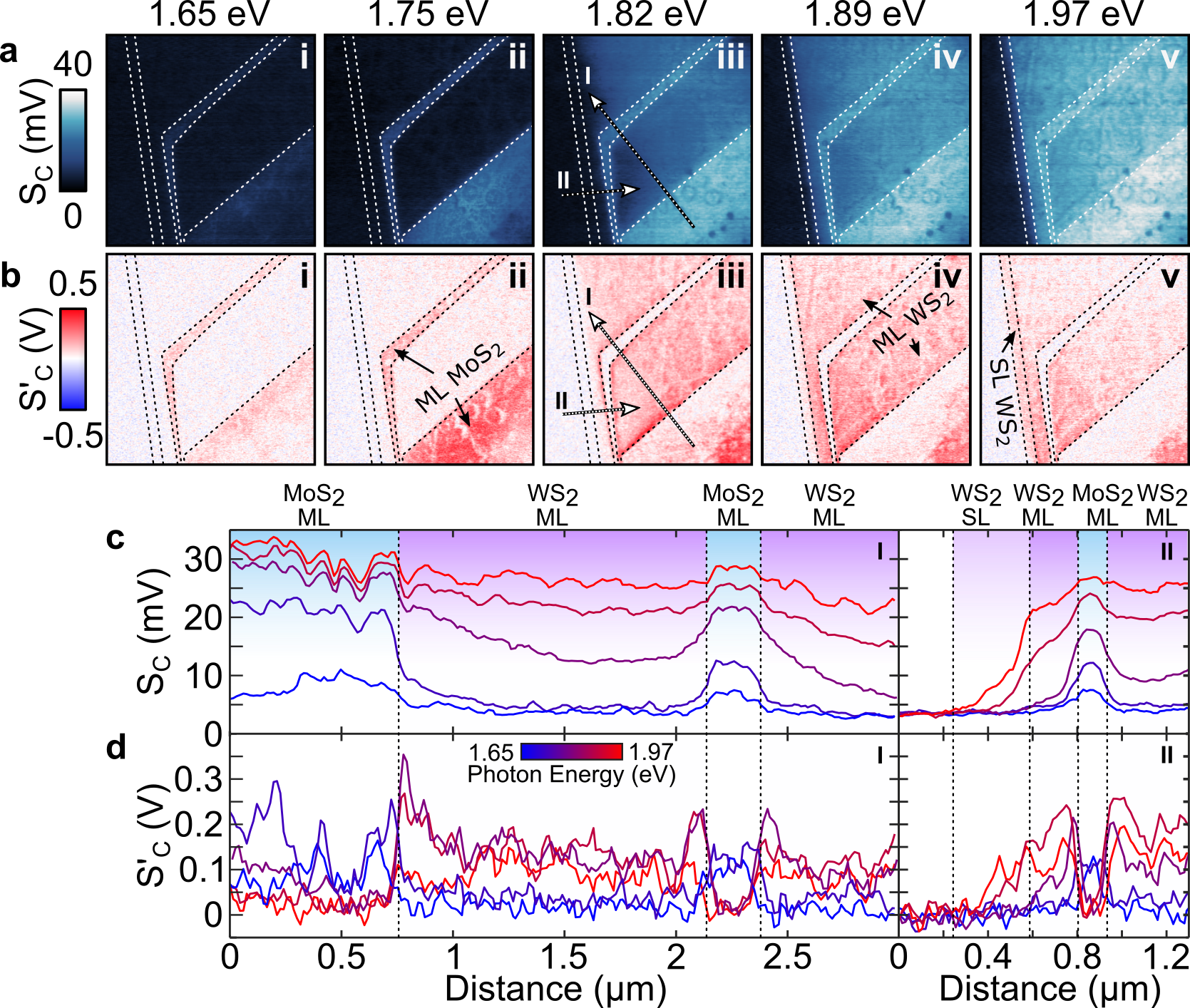
For examining the interface, we note that while we cannot directly probe the interfacial band alignment in these electrically isolated heterostructures, we can probe both the carrier density and type across the interfaces by examining high-resolution images of the interfacial regions. Shown in Fig 4a are the photon energy-dependent SC images of the region of flake 1 enclosed by the dashed square in Figure 2fiv, with the domain boundaries indicated by dashed lines. As expected from Figure 2f, as the photon energy is increased the ML MoS2 domain becomes photoconductive first, followed by the ML WS2 domain, and lastly photoconductivity becomes discernible in the thin SL WS2 domain at the flake edge at 1.97 eV.
The S images shown in Figure 4b provide complementary information to the SC images. At low photon energies, we see that the S signal increases in parallel with the SC signal. As the photon energy is increased, regions of higher SC such as the ML MoS2 domains show a diminished S signal as expected for higher carrier densities 42, 43. It should be noted that the S measurement probes the high-frequency branch of the capacitance-voltage (C-V) curve 44. As such, any work function difference between our platinum tips and the doped sample does not invert the carrier type, but rather shifts the flat-band voltage while maintaining the sign of the C-V curve slope 43.
Confirming the whole-flake S image in Figure 2f, the sign of the S channel in Figure 4b remains positive throughout, indicating that the conductivity in both materials remains dominated by the same carrier type. Transport in MoS2 is generally observed to be n-type in few-layer devices 19, 45, 29, although this can be influenced by the presence of Schottky barriers at the contacts 46. As further discussed below, photocharging in MoS2 – which occurs independent of electrode Schottky barriers – is consistently observed to be n-type. Previous transport measurements of the MoS2 regions of identically grown flakes also showed n-type transport after control for Schottky barriers 27, 28. Based on the S signal we therefore conclude that the WS2 is most likely n-type throughout these electrically isolated photoexcited flakes as well.
Careful examination of the interface suggests electron transfer from the MoS2 to the WS2. Shown in Figure 4c and d are the line cuts taken along the dashed arrows in Fig 4biii where the approximate positions of the interfaces is estimated based on the photon energy-dependent photoconductivity onset. In particular, the conductivity change across the ML MoS2–WS2 interface appears to be abrupt at lower (1.65 eV and 1.75 eV) and higher (1.97 eV) photon energies. However, at 1.82 eV and to a lesser degree at 1.89 eV, the n-type conductivity in the ML WS2 region is highest at the MoS2–WS2 interface and decays away from the interface. This decay appears to occur over a length scale of 100 – 250 nm away from the interface, which is an order of magnitude shorter than measured depletion regions seen for MoS2–WS2 type-II alignment 36 and indicates a different origin. Given that this interfacial photoconductivity is observed to be strongest under resonant excitation of the ML MoS2 domain at 1.82 eV where the WS2 absorption is weak, this strongly suggests that these carriers originate in the MoS2. This observed increased photoconductivity in the WS2 region can be explained by the steady-state diffusion of electrons injected into the WS2 from the MoS2.
This charge transfer can occur by several possible mechanisms driven by the accumulation of electrons in the MoS2. If the conduction bands are energetically close to each other (i.e., the band offset is shifted by a few 100 meV relative to a type-II junction), direct charge transfer could occur. Alternatively, the decay of an exciton in the MoS2 could readily impart sufficient energy on a free carrier to overcome interfacial barriers via an Auger-type mechanism. In the case of type-II alignment, this charge transfer could also be indirectly mediated by interfacial excitons. Here, an electron in the MoS2 can bind with either an exciton or the hole of a dissociated exciton in the WS2 to form an interfacial trion or exciton, respectively. The decay of this interfacial species would then leave behind an excess electron in the WS2 conduction band. We note that the latter hypothesis is also supported by the observation that no interfacial conductivity is seen in the WS2 at photon energies of 1.75 eV and lower despite the apparent accumulation of carriers in the MoS2. It thus seems likely that some absorption in the WS2 (i.e., exciton generation) is necessary to drive this effect. This mechanism could occur in any sufficiently sharp type-II junction supporting interfacial excited bound states such a excitons in van der Waals materials or charge transfer states in small molecule-TMD interfaces 47.
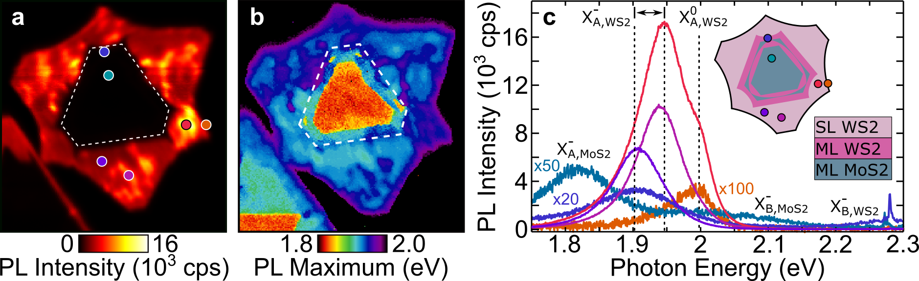
Having addressed the electronic characteristics and their spatial inhomogeneities in these samples under photoexcitation, we now directly compare these with spatially resolved PL maps. Shown in Figure 5a is the spatially resolved PL map of flake 2 at an emission energy of 1.97 eV (630 nm), and the PL peak emission photon energy at each spatial location is shown in b. A schematic of the different regions of the flake are shown in the inset of Figure 5c. Together with the SMM images in Figure 3 and the discrete PL spectra in Figure 5c that are taken from the indicated positions in Figure 5a and the inset, we find that our SL WS2 domains contain three distinct regions. The very edges of our flakes show asymmetrically broadened weak emission with a high-energy PL peak around 1.99 eV and very little discernible local conductivity. This observed edge emission at 1.99 eV is the highest energy transition observed here, which we assign to the neutral A-exciton X in good agreement with literature values and corroborated by the low local photoconductivity 6, 30. In contrast, much of the WS2 SL domain interior shows strong emission with a spectral maximum at around 1.91 eV and significant conductivity. Lastly, we see localized regions within the SL domain that show emission up to 3x stronger than other interior regions and an emission maximum around 1.94 eV. These strongly emitting regions correspond to the weakly photoconductive regions in Figure 3c and d. Accordingly, the emission in the interior of the SL portion of the flake corresponds to the negatively charged trion X. The spatial variations in X show a correlation between a decrease in emission energy and increasing carrier density 5, with the low-conductivity regions revealing the superposition of X and X expected from regions nearing charge-neutrality 30.
While the PL characteristics of the ML MoS2 domain are uniformly weak and without discernible shift in the peak position, the ML WS2 domains also contain regions with lower photoconductivity and a significant blueshift in the PL peak. We also found no evidence of interfacial excitons to support our hypothesis of interfacial exciton-mediated charge transfer, though given the overall weak emission from the ML regions and the difference in excitation photon energy between the PL measurements (2.38 eV) and the interfacial conductivity observed with 1.82 eV excitation, this is not surprising.
Discussion
Our observations directly confirm that within the SL WS2 domains a locally reduced free carrier density leads to a blueshift in the PL peak and an increase in the PL efficiency 9, 7. Importantly, it is highly unlikely that the increased radiative decay rate is responsible for the reduced charging in the damaged regions. Rather, the increased radiative decay rate is either the likely result of a low carrier density that results from passivated hole traps or the direct result of damage-related radiative recombination centers. Any damage and related effects were likely incurred prior to SMM measurements, where we were careful to perform SMM characterization prior to PL measurements to minimize photoinduced damage. We observed no photo-induced degradation 48 during repeated measurement sequences over several weeks.
Persistent photoconductivity is a well-known semiconductor phenomenon and arises from defects that give rise to long-lived traps 49. Persistent photoconductivity has been reported 17, 16, 18, 50 and deliberately engineered 51 in MoS2 devices. This effect appears to consistently result in an accumulation of n-type carriers and is primarily driven by extrinsic interfacial traps at the MoS2/SiO2 interface 17, 16, 18, and the disappearance of long-lived traps leading to hysteresis on hexagonal boron nitride (hBN) substrates 52 further support this conclusion. Although exfoliated and CVD-grown TMDs have intrinsic defect densities of up to 1013 cm-2 53, 54 that adversely affect transport 55, these do not appear to directly produce long-lived traps, but rather facilitate their formation by providing chemically active sites for, e.g., oxygen adsorbates 17. However, the role of these active sites on the otherwise chemically inert TMD surface in mediating the formation of extrinsic traps remains unclear.
We estimate the local carrier densities by noting that under illumination at 1.97 eV the interior ML domains in Figures. 2 and 3 show little signal variation in the SG images although clear variations remain in the SC images. This suggests that the conductivity is at the plateau region of the SG branch of Figure 2A. In contrast, under dark conditions the flake conductivity is uniformly at or below the instrumental detection limit, corresponding to a photoinduced increase in the conductivity by 200 times. Therefore, assuming carrier density-independent mobility and a carrier density near the detection limit, our finite element modeling indicates that at moderate optical intensities the carrier densities in regions of our structure is increased by a factor of up to 200
As mobilities can be difficult to extract from two-terminal transport measurements and electrode deposition would likely damage our flakes, we assume a mobility of 5 – 10 cm2/Vs to estimate carrier densities, representative of CVD-grown MoS2 55. For the interior BL regions, the photoexcited conductivity at the SG plateau of 2 103 S/m corresponds to n 1.6 – 3.2 1012 cm-2, while the detection limit of 10 S/m corresponds to n 8 109 cm-2. We note that this estimated dark carrier density is low given the high intrinsic defect density of these materials, suggesting that the dark conductivity is not significantly below the instrumental sensitivity limit.
This persistent charging appears to occur more broadly in MoS2 and has significant implications for any measurement requiring prolonged optical illumination at photon energies at or above the onset of excitonic absorption - including below the electronic bandgap. This implies that such measurements do not probe the intrinsic dark state but rather reflect a heavily modified metastable optically excited state. Our results thus emphasize that optical measurements of MoS2 and associated heterostructures that are sensitive to the free carrier density need be interpreted with caution and likely do not reflect the intrinsic sample itself. However, the capability to develop spatially structured engineered trap storage devices 51 aided by SMM imaging could also lead to novel memory and switching functionalities.
The large spatial variations in both PL peak position and intensity are characteristic of CVD-grown TMD sheets in general 12 and a range of observations are reported for SL WS2 in particular 48, 8, 10, 56. These results generally show a distinct PL intensity difference between the flake edge or near-edge region and the interior. These variations are often directly correlated with a discernible shift in the emission peak that is attributed to spatial change in the X and X exciton emission due to local carrier density. Here we can directly corroborate these assignments, which underscores the unique capability of SMM to directly access the local conductive and photoconductive behavior in electrically insulated samples in a nondestructive manner.
Lastly, we point out that despite the large exciton binding energies of up to several 100s of meV 30, the free carriers that contribute to the microwave admittance are nonetheless generated 23. This effect has been clearly established for low-dimensional systems supporting tightly-bound excitons using time-resolved microwave conductivity (TRMC) 57. And although the mechanism remains unclear, recent results from WS2 flakes suggest a prominent role for ML regions in the formation of free carriers possibly due to reduced exciton binding energy and traps at lateral interfaces 41.
Conclusions
In this work, we have used photon energy-resolved photoconductivity mapping to study the spatial photoconductivity distribution and long-term carrier accumulation in MoS2–WS2 lateral multijunction heterostructures.
We reveal that the optoelectronic response is dominated by photoinduced n-type charging that can increase the local carrier density by over two orders of magnitude and can persist for up to several days.
This confirms that the tightly bound excitons in TMDs can nonetheless dissociate into free carriers, which challenges the assumption that optical excitation below the electronic bandgap does not significantly change the carrier density.
Through correlated photoluminescence mapping, we confirm that spatial variations in carrier density directly affect the emission intensity as well as the spectral peak position via the interplay between neutral excitons and carrier bound excitons (trions).
This work underscores the need for spatially resolved characterization in 2D systems and cautions that optical measurements – particularly of 2D MoS2 on SiO2 – can persistently modify the sample studied during the measurement process and likely reflect a metastable charged state rather than the true dark ground state.
Our results clearly demonstrate the potential of microwave near-field microscopy to probe the local variations in the potential energy landscape as it affects carrier motion, which has allowed us to address the interplay between optical and electronic properties.
Methods
Heterostructure Sample. MoS2–WS2 lateral multijunction heterostructures were grown using a one-pot chemical vapor deposition method described previously 27, 28. On order to accommodate through-sample illumination, the samples were then transferred to an optically transparent quartz substrate using a solution-based poly(methyl methacrylate) (PMMA)–mediated transfer 58. Isolated flakes are chosen for study using an optical microscope. MoS2 and WS2 domains within the flakes as well as single layer regions are confirmed using spatially resolved photoluminescence imaging using 532 nm (2.38 eV) illumination.
Optical Microwave Near-Field Microscopy. The SMM is based on a commercial AFM/SMM (Agilent/Keysight 5500*). As described previously 26, the system is modified to accommodate external IQ mixer-based microwave demodulation. All measurements are performed with the AFM operating in contact mode using SMM-specific solid Pt cantilevers (Rocky Mountain Nanotechnology 25Pt300A*).
The optical excitation is based on a broadband supercontinuum source (Fianium*). The continuously tunable excitation source is generated from the broadband supercontinuum spectrum by spectral shaping using a razor blade slit mounted on a translation stage and placed at the shaper Fourier plane. After spectral shaping, the light is coupled into a multimode fiber and delivered to the sample by illumination through the substrate from below. In order to provide uniform optical excitation across the tip-scanned region and maintain linear excitation densities, the fiber termination is placed immediately below the transparent substrate and the beam allowed to diverge. This produces an excitation spot at the sample with radius 100 m and intensity 2 W/cm2.
Finite-Element Modeling.
The finite-element modeling was performed using COMSOL 4.4* as previously described in the literature59, 29, 23.
Briefly, the we use the AC/DC module with an axisymmetric geometry at our experimental frequency of 17.2 GHz.
The experimental geometry is modeled with a TMD flake ( = 7) with thickness of 0.65 nm (SL) or 1.3 nm (BL) and variable conductivity on a quartz substrate ( = 3.9).
We use a parabolic tip shape with an apex radius of 20 nm that is held 1 nm above the substrate to facilitate meshing.
*Mention of commercial products is for informational purposes only, it does not imply NIST’s recommendation or endorsement.
Supporting Information Available
Optical micrographs of lateral heterostructures (Figure S1); Optical and PL maps of flakes 1 and 2 (Figure S2); Photon-energy dependent conductivity of an additional flake (Figure S3); Correction of capacitive topographic cross-talk (Figure S4); Full photo-induced charging and discharging dataset for flake 2 (Figure S5); Decay of persistent photoconductivity of flake 1 (Figure S6); Verification of lack of charge transfer from tip (Figure S7); Photoconductivity of individual MoS2 and WS2 lateral heterojunctions (Figure S8).
Acknowledgements
We would like to acknowledge valuable discussions with Nicholas J. Borys and Obadiah G. Reid. HZ, JLB, EMM, and SUN are employees of the Alliance for Sustainable Energy, LLC, the manager and operator of the National Renewable Energy Laboratory for the U.S. Department of Energy under Contract No. DE-AC36-08GO28308. Funding provided by U.S Department of Energy, Office of Science, Office of Basic Energy Sciences, Division of Chemical Sciences, Geosciences and Biosciences. The views expressed in the article do not necessarily represent the views of the Department of Energy or the U.S. Government. Contributions of the US Government are not subject to copyright in the United States.
References
- Spendiani et al. 2010 Spendiani, A.; Sun, L.; Zhang, Y.; Li, T.; Kim, J.; Chim, C. Y.; Galli, G.; Wang, F. Emerging Photoluminescence in Monolayer MoS2. Nano Lett. 2010, 10, 1271–1275
- Mak et al. 2010 Mak, K. F.; Lee, C.; Hone, J.; Shan, J.; Heinz, T. F. Atomically Thin MoS2: A New Direct-Gap Semiconductor. Phys. Rev. Lett. 2010, 105, 136805
- Mak et al. 2014 Mak, K. F.; McGill, K. L.; Park, J.; McEuen, P. L. The valley hall effect in MoS2 transistors. Science 2014, 344, 1489–1492
- Li et al. 2018 Li, Z.; Wang, T.; Lu, Z.; Jin, C.; Chen, Y.; Meng, Y.; Lian, Z.; Taniguchi, T.; Watanabe, K.; Zhang, S.; Smirnov, D.; Shi, S. F. Revealing the biexciton and trion-exciton complexes in BN encapsulated WSe2. Nat. Commun. 2018, 9, 3719
- Mak et al. 2012 Mak, K. F.; He, K.; Lee, C.; Lee, G. H.; Hone, J.; Heinz, T. F.; Shan, J. Tightly bound trion in monolayer MoS2. Nat. Mater. 2012, 12, 207–211
- Mitioglu et al. 2013 Mitioglu, A. A.; Plochocka, P.; Jadczak, J. N.; Escoffier, W.; Rikken, G. L. J. A.; Kulyuk, L.; Maude, D. K. Optical manipulation of the exciton charge state in single layer tungsten disulfide. Phys. Rev. B 2013, 88, 245403
- Lien et al. 2019 Lien, D. H.; Uddin, S. Z.; Yeh, M.; Amani, M.; Kim, H.; Ager III, J. W.; Yablanovitch, E.; Javey, A. Electrical suppression of all nonradiative recombination pathways in monolayer semiconductors. Science 2019, 364, 468–471
- Hu et al. 2019 Hu, Z.; Avila, J.; Wang, X.; Leong, J. F.; Zhang, Q.; Liu, Y.; Asensio, M. C.; Lu, J.; Carvalho, A.; Sow, C. H.; Castro Neto, A. H. The role of oxygen atoms on excitons at the edges of monolayer WS2. Nano Lett. 2019, 19, 4641–4650
- Nan et al. 2014 Nan, H.; Wang, Z.; Wang, W.; Lian, Z.; Lu, Y.; Chen, Q.; He, D.; Tan, P.; Miao, F.; Wang, X.; Wang, J.; Ni, Z. Strong photoluminescence enhancement of MoS2 through defect engineering and oxygen bonding. ACS Nano 2014, 8, 5738–5745
- Yao et al. 2018 Yao, H.; Liu, L.; Wang, Z.; Li, H.; Chen, L.; Pam, M. E.; Chen, W.; Yang, H. Y.; Zhang, W.; Shi, Y. Significant photoluminescence enhancement in WS2 monolayers through Na2S treatment. Nanoscale 2018, 10, 6105–6112
- Tanoh et al. 2019 Tanoh, A.; Alexander-Webber, J.; Xiao, J.; Delport, G.; Williams, C. A.; Bretscher, H.; Gauriot, N.; Allardice, J.; Pandya, R.; Fan, Y.; Li, Z.; Vignolini, S.; Stranks, S. D.; Hofmann, S.; Rao, A. Enhancing photoluminescence and mobilities in WS2 monolayers with oleic acid ligands. Nano Lett. 2019, 19, 6299–6307
- Zhang et al. 2017 Zhang, K.; Borys, N.; Bersch, B.; Bhimanapati, G.; Xu, K.; Wang, B.; Wang, K.; Labella, M.; Williams, T.; Haque, M.; Barnard, E.; Fullerton-Shirey, S.; Schuck, P.; Robinson, J. Deconvoluting the photonic and electronic response of 2D materials: The case of MoS2. Sci. Rep. 2017, 7, 16938
- Sahoo et al. 2019 Sahoo, P. K.; Zong, H.; Liu, J.; Xue, W.; Lai, X.; Gutiérrez, H. G.; Voronine, D. V. Probing nano-heterogeneity and aging effects in lateral 2D heterostructures using tip-enhanced photoluminescence. Opt. Mater. Express 2019, 9, 1620–1631
- Park et al. 2016 Park, K. D.; Khatib, O.; Kravtsov, V.; Clark, G.; Xu, X.; Raschke, M. B. Hybrid tip-enhanced nanospectroscopy and nanoimaging of monolayer WSe2 with local strain control. Nano Lett. 2016, 16, 2621–2627
- Bao et al. 2015 Bao, W.; Borys, N. J.; Ko, C.; Suh, J.; Fan, W.; Thron, A.; Zhang, Y.; Buyanin, A.; Zhang, J.; Cabrini, S.; Ashby, P. D.; Weber-Bargioni, A.; Tongay, S.; Aloni, S.; Ogletree, D. F.; Wu, J.; Salmeron, M. B.; Schuck, P. J. Visualizing nanoscale excitonic relaxation properties of disordered edges and grain boundaries in monolayer molybdenum disulfide. Nat. Commun. 2015, 6, 7993
- Di Bartolomeo et al. 2017 Di Bartolomeo, A.; Genovese, L.; Foller, T.; Giubileo, F.; Luongo, G.; Croin, L.; Liang, S. J.; Ang, L. K.; Schleberger, M. Electrical transport and persistent photoconductivity in monolayer MoS2 phototransistors. Nanotechnology 2017, 28, 214002
- Wu et al. 2015 Wu, Y. C.; Liu, C. H.; Chen, S. Y.; Shih, F. Y.; Ho, P. H.; Chen, C. W.; Liang, C. T.; Wang, W. H. Extrinsic origin of persistent photoconductivity in monolayer MoS2 field effect transistors. Sci. Rep. 2015, 2, 11472
- Cho et al. 2014 Cho, K.; Kim, T. Y.; Park, W.; Park, J.; Kim, D.; Jang, J.; Jeong, H.; Hong, S.; Lee, T. Gate-bias stress-dependent photoconductive characteristics of multi-layer MoS2 field-effect transistors. Nanotechnology 2014, 25, 155201
- Radisavljevic et al. 2011 Radisavljevic, B.; Radenovic, A.; Brivio, J.; Giacometti, V.; Kis, A. Single-layer MoS2 transistors. Nat. Nanotechnol 2011, 6, 147–150
- Li et al. 2015 Li, M. Y.; Shi, Y.; Cheng, C. C.; Lu, L. S.; Lin, Y. C.; Tang, H. L.; Tsai, M. L.; Chu, C. W.; Wei, K. H.; He, J. H.; Chang, W. H.; Suenaga, K.; K, L. J. Epitaxial growth of a monolayer WSe2-MoS2 lateral p-n junction with an atomically sharp interface. Science 2015, 349, 524–528
- Sun et al. 2019 Sun, T.; Zhang, H.; Wang, X.; Liu, J.; Xiao, C.; Nanayakkara, S. U.; Blackburn, J. L.; Mirkin, M. V.; Miller, E. M. Nanoscale mapping of hydrogen evolution on metallic and semiconducting MoS2 nanosheets. Nanoscale Horiz. 2019, 4, 619–624
- Dagan et al. 2019 Dagan, R.; Vaknin, Y.; Henning, A.; Shang, J. Y.; Lauhon, L. J.; Rosenwaks, Y. Two-dimensional charge carrier distribution in MoS2 monolayer and multilayers. Appl. Phys. Lett. 2019, 114, 101602
- Tsai et al. 2017 Tsai, Y.; Chu, Z.; Han, Y.; Chuu, C. P.; Wu, D.; Johnson, A.; Cheng, F.; Chou, M. Y.; Muller, D. A.; Li, X.; Lai, K.; Shih, C. K. Tailoring semiconductor lateral multijunctions for giant photoconductivity enhancement. Adv. Mater. 2017, 29, 1703680
- Johnston et al. 2018 Johnston, S. R.; Ma, E. Y.; Shen, Z. X. Optically coupled methods for microwave impedance microscopy. Rev. Sci. Instrum. 2018, 89, 043703
- Chu et al. 2018 Chu, Z.; Han, A.; Lei, C.; Lopatin, S.; Li, P.; Wannlund, D.; Wu, D.; Herrera, K.; Zhang, X.; MacDonald, A. H.; Li, X.; Li, L. .-J.; Lai, K. Energy-resolved photoconductivity mapping in a monolayer-bilayer WSe2 heterostructure. Nano Lett. 2018, 18, 7200–7206
- Berweger et al. 2019 Berweger, S.; Qiu, G.; Wang, Y.; Pollard, B.; Genter, K. L.; Tyrrell-Ead, R.; Wallis, T. M.; Wu, W.; Ye, P.; Kabos, P. Imaging carrier inhomogeneities in ambipolar tellurene field-effect transistors. Nano Lett. 2019, 19, 1289–1294
- Sahoo et al. 2018 Sahoo, P. K.; Memarian, S.; Xin, Y.; Balicas, L.; Gutiérrez, H. R. One-pot growth of two-dimensional lateral heterostructures via sequential edge-epitaxy. Nature 2018, 553, 63–67
- Sahoo et al. 2019 Sahoo, P. K.; Memaran, S.; Nugera, F. A.; Xin, Y.; Márquez, T. D.; Lu, Z.; Zheng, W.; Zhigadlo, N. D.; Smirnov, D.; Balicas, L.; Rodríguez Gutíerrez, H. Bilayer lateral heterostructures of transition-metal dichalcogenides and their optoelectronic response. ACS Nano 2019, 13, 12372–12384
- Berweger et al. 2015 Berweger, S.; Weber, J. C.; John, J.; Velazquez, J. M.; Pieterick, A.; Sanford, N. A.; Davydov, A. V.; Brunschwig, B.; Lewis, N. S.; Wallis, T. M.; Kabos, P. Micowave Near-Field Imaging of Two-Dimensional Semiconductors. Nano Lett. 2015, 15, 1122–1127
- Zhu et al. 2015 Zhu, B.; Chen, X.; Cui, X. Exiton binding energy of monolayer WS2. Sci. Rep. 2015, 5, 9218
- Borys et al. 2017 Borys, N.; Barnard, E. S.; Gao, S.; Yao, K.; Bao, W.; Buyanin, A.; Zhang, Y.; Tongay, S.; Ko, C.; Suh, J.; Weber-Bargioni, A.; Wu, J.; Yang, L.; Schuck, P. J. Anomalous above-gap photoexcitations and optical signatures of localized charge puddles in monolayer molybdenum disulfide. ACS Nano 2017, 11, 2115–2123
- Zhang et al. 2015 Zhang, D. X.; Qiao, X. F.; Shi, W.; Wu, J. B.; Jiang, D. S.; Tan, P. H. Phonon and Raman scattering of two-dimensional transition metal dichalcogenides from monolayer, multilayer to bulk material. Chem. Soc. Rev. 2015, 44, 2757
- Coakley et al. 2019 Coakley, C. J.; Berweger, S.; Wallis, T. M.; Kabos, P. Disentangling topographic contributions to near-field scanning microwave microscopy images. Ultramicroscopy 2019, 197, 53–64
- Tang et al. 2018 Tang, C.; He, Z.; Chen, W.; Jia, S.; Lou, J.; Voronine, D. Quantum plasmonic hot-electron injection in lateral WSe2/MoSe2 heterostructures. Phys. Rev. B 2018, 98, 041402(R)
- Gong et al. 2014 Gong, Y.; Lin, J.; Wang, X.; Shi, G.; Lei, S.; Lin, Z.; Zou, X.; Ye, G.; Vjtai, R.; Yakobson, B. I.; Terrones, H.; Terrones, M.; Tay, B. K.; Lou, J.; Pantalides, S. T.; Liu, Z.; Zhou, W.; Ajayan, P. M. Vertical and in-plane heterostructures from WS2/MoS2 monolayers. Nat. Mater. 2014, 13, 1135–1142
- Chen et al. 2015 Chen, K.; Wan, X.; Wen, J.; Xie, W.; Kang, Z.; Zeng, X.; Chen, H.; Xiu, J. B. Electronic properties of MoS2-WS2 heterostructures synthesized with two-step lateral epitaxial strategy. ACS Nano 2015, 9, 9868–9876
- Hill et al. 2016 Hill, H. M.; Rigosi, A. F.; Rim, K. T.; Flynn, G. W.; Heinz, T. F. Band alignment in MoS2/WS2 transition metal dichalcogenide heterostructures probed by scanning tunneling microscopy and spectroscopy. Nano Lett. 2016, 16, 4831–4837
- Zhang et al. 2018 Zhang, C.; Li, M. Y.; Tersoff, J.; Han, Y.; Su, Y.; Li, L. J.; Muller, D. A.; Shih, C. K. Strain distributions and their influences on electronic structures of WSe2-MoS2 laterally strained heterojunctions. Nat. Nanotechnol. 2018, 13, 152–158
- Yang et al. 2017 Yang, Y.; Fang, W. H.; Long, R. Disparity on photoexcitation dynamics between vertical MoS2/WS2 heterojunctions: Time-domain simulation emphasizes the importance of donor-acceptor interaction and band alignment. J. Phys. Chem. Lett. 2017, 8, 5771–5771
- Kang et al. 2015 Kang, J.; Sahin, H.; Peeters, F. M. Tuning carrier confinement in the MoS2/WS2 lateral heterostructure. J. Phys. Chem. C 2015, 119, 9580–9586
- Blackburn et al. 2020 Blackburn, J. L.; Zhang, H.; Myers, A. R.; Dunklin, J. R.; Coffey, D. C.; Hirsch, R. N.; Vigil-Fowler, D.; Yun, S. J.; Cho, B. W.; Lee, Y. H.; Miller, E. M.; Rumbles, G.; Reid, O. G. Measuring photoexcited free charge carriers in mono-to few-layer transition-metal dichalcogenides with steady-state microwave conductivity. J. Phys. Chem. Lett. 2020, 11, 99–107
- Huber et al. 2012 Huber, H. P.; Humer, I.; Hochleitner, M.; Fenner, M.; Moertelmaier, M.; Rankl, C.; Imtiaz, A.; Wallis, T. M.; Tanbakuchi, H.; Hinterdorfer, P.; Kabos, P.; Smoliner, J.; Kopanski, J. J.; Kienberger, F. Calibrated nanoscale dopant profiling using a scanning microwave microscope. J. Appl. Phys. 2012, 111, 014301
- Edwards et al. 2000 Edwards, H.; Ukraintsev, V. A.; San Martin, R.; Johnson, F. S.; Menz, P.; Walsh, S.; Ashburn, S.; Wills, K. S.; Harvey, K.; Chang, M. C. pn-junction delineation in Si devices using scanning capacitance spectroscopy. J. Appl. Phys. 2000, 87, 1485–1495
- Sze and Ng 2007 Sze, S.; Ng, K. Semiconductor Devices; John Wiley Sons, 2007
- Bao et al. 2013 Bao, W.; Cai, X.; Kim, D.; Sridhara, K.; Fuhrer, M. S. High mobility ambipolar MoS2 field-effect transistors: Substrate and dielectric effects. Appl. Phys. Lett. 2013, 102, 042104
- Liu et al. 2018 Liu, Y.; Guo, J.; Zhu, E.; Liao, L.; Lee, S. J.; Ding, M.; Shakir, I.; Gambin, V.; Huang, Y.; Duan, X. Approaching the Schottky-Mott limit in van der Waals metal-semiconductor junctions. Nature 2018, 557, 696–700
- Zhu et al. 2018 Zhu, T.; Yuan, L.; Zhao, Y.; Zhou, M.; Wan, Y.; Mei, J.; Huang, L. Highly mobile charge-transfer excitons in two-dimensional WS2/tetracene heterostructures. Sci. Adv. 2018, 4, eaao3104
- Kotsakidis et al. 2019 Kotsakidis, J. C.; Zhang, Q.; Vasquez de Parga, A. L.; Currie, M.; Helmerson, K.; Gaskill, D. K.; Fuhrer, M. S. Oxidation of Monlayer WS2 in Ambient is a Photoinduced Process. Nano Lett. 2019, 19, 5205–5215
- Lang and Logan 1977 Lang, D. V.; Logan, R. A. Large–Lattice-Relaxation Model for Persistent Photoconductivity in Compound Semicondctors. Phys. Rev. Lett. 1977, 39, 635–639
- Lopez-Sanchez et al. 2013 Lopez-Sanchez, O.; Lembke, D.; Kayci, M.; Radenovic, A.; Kis, A. Ultrasensitive photodetectors based on monolayer MoS2. Nat. Nanotechnol. 2013, 8, 497–501
- Lee et al. 2017 Lee, J.; Pak, S.; Lee, Y. W.; Cho, Y.; Hong, J.; Giraud, P.; Shin, H. S.; Morris, S. M.; Sohn, J. I.; Cha, S. N.; Kim, J. M. Monolayer optical memory cells based on artificial trap-mediated charge storage and release. Nat. Commun. 2017, 8, 14734
- Lee et al. 2013 Lee, G. H.; Yu, Y. J.; Cui, X.; Petrone, N.; Lee, C. H.; Choi, M. S.; Lee, D. Y.; Lee, C.; Yoo, W. J.; Watanabe, K.; Taniguchi, T.; Nuckolls, C.; Kim, P.; Hone, J. Flexible and transparent MoS2 field-effect transistors on hexagonal boron nitride-graphene heterostructures. ACS Nano 2013, 7, 7931–7936
- Edelberg et al. 2019 Edelberg, D.; Rhodes, D.; Kerelsky, A.; Kim, B.; Wang, J.; Zangiabadi, A.; Kim, C.; Abhinadan, A.; Ardelean, J.; Scully, M.; Scullion, D.; Embon, L.; Zu, R.; Santos, E. J. G.; Balicas, L.; Marianetti, C.; Barmak, K.; Zhu, X.; Hone, J.; Pasupathy, A. N. Approaching the intrinsic limit in transition metal diselenides via point defect control. Nano Lett. 2019, 19, 4371–4379
- Hong et al. 2015 Hong, J.; Hu, Z.; Probert, M.; Li, K.; Lv, D.; Yang, X.; Gu, L.; Mao, N.; Feng, Q.; Xie, L.; Zhang, J.; Wu, D.; Zhang, Z.; Jin, C.; Ji, W.; Zhang, X.; Yuan, J.; Zhang, Z. Exploring atomic defects in molybdenum disulphide monolayers. Nat. Commun. 2015, 6, 6293
- Rhodes et al. 2019 Rhodes, D.; Chae, S. H.; Ribeiro-Palau, R.; Hone, J. Disorder in van der Waals heterostructures of 2D materials. Nat. Mater. 2019, 18, 541–549
- Gutiérrez et al. 2012 Gutiérrez, H.; Perea-López, N.; Elías, A. L.; Berkdemir, A.; Wang, B.; Lv, R.; López-Urías, F.; Crespi, V. H.; Terrrones, H.; Terrones, M. Extraordinary room-temperature photoluminescence in triangular WS2 monolayers. Nano Lett. 2012, 12, 3447–3454
- Park et al. 2015 Park, J.; Reid, O. G.; Blackburn, J. L.; Rumbles, G. Photoinduced spontaneous free-carrier generation in semiconducting single-walled carbon nanotubes. Nat. Commun. 2015, 6, 8809
- Her et al. 2013 Her, M.; Beams, R.; Novotny, L. Graphene transfer with reduced residue. Phys. Lett. A 2013, 377, 1455–1458
- Kundhikanjana et al. 2009 Kundhikanjana, W.; Lai, K.; Wang, H.; Dai, H.; Kelly, M. A.; Shen, Z. X. Hierarchy of electronic properties of chemically derived and pristine graphene probed by microwave imaging. Nano Lett. 2009, 9, 3762–3765