van der Waals coefficients of the multi-layered MoS2 with alkali metals
Abstract
The van der Waals coefficients and the separation dependent retardation functions of the interactions between the atomically thin films of the multi-layered transition metal molybdenum disulfide (MoS2) dichalcogenides with the alkali atoms are investigated. First, we determine the frequency-dependent dielectric permittivity and intrinsic carrier density values for different layers of MoS2 by adopting various fitting models to the recently measured optical data reported by Yu and co-workers [Sci. Rep. 5, 16996 (2015)] using spectroscopy ellipsometry. Then, dynamic electric dipole polarizabilities of the alkali atoms are evaluated very accurately by employing the relativistic coupled-cluster theory. We also demonstrate the explicit change in the above coefficients for different number of layers. These studies are highly useful for the optoelectronics, sensing and storage applications using layered MoS2.
I Introduction
Recent advances in the fabrication and synthesis of ultra-thin layered materials with unit cell thickness has boosted the art of continuously tailoring the properties of materials. Among these, graphene, a two dimensional (2D) material of carbon atoms, exhibit unique electronic, physical and chemical properties. However, zero band gap of graphene restricts the direct application of graphene in the electronic devices. This has prompted to search for composite graphene-like materials with a finite band gap. Transition metal dichalcogenides (TMDs) possessing the identical lamellar structure of graphite manifest remarkable applications in nano-electronics, sensors, catalytic, energy conversion and storage devices. The nature of transition elements present in these materials affects their structures. TMDs containing transition elements from the IV-VII groups of the periodic table exhibit layered structures, while those containing transition elements belonging to the VIII-X groups show non-layered structures han2015 .
In addition to the homo-layer configurations in the 2D TMDs, the nanoscale heterostructures of TMDs have also been found to be suitable for the implementation of novel photonic and electronic devices gong2013 ; komsa2013 . Theoretical studies demonstrate that several 2D TMDs offer a plethora of opportunities using lateral and vertical heterostructures due to their tunable broad-range optical bandgap and strong light-matter interactions pksahoo1 ; pksahoo2 . These heterostructures can be classified into three types on the basis of their band alignments; i.e. symmetric (type I), staggered (type II) and broken (type III) ozcelik . All these materials find many applications in high performance devices such as light-emitting diodes, photodetectors and transistors withers2015 ; xu2017 ; nakamura1995 ; yu2013 ; zhang2011 ; sarkar2015 ; lin2015 ; koswata2010 . Moreover, strong Coulomb interactions and anisotropic dielectric environment lead to the formation of strongly bound excitons, trions, and biexcitons in these materials you2015 ; he2014 ; mak2012 . The hetero-bilayers of TMDs with inter-layer excitons are emerging as novel class of long-lived dipolar composite bosons for optoelectronic applications kremser2020 . Recently, it has been found that magnetic fields can promote the formation of biexciton to create favorable conditions for the formation of multiple exciton complexes, exciton super-fluidity, and biexciton condensates to materialize their practical applications stevens2018 .
Among TMDs, molybdenum disulfide (MoS2) has emerged as one of the promising next-generation 2D materials with exceptional photonic, non-linear and electronic properties, in contrast to its bulk counterpart Q.H.Wang2012 ; Chhowalla2013 ; Li2015 and attracted applications among flexible gas sensing Donarelli2018 ; Akbari2018 and optoelectronic devices Mak2010 ; Brasch2016 ; Tsai2014 ; Yin2012 ; Guo2016 ; Tongay2012 ; Gutuerrez2013 ; Sundaram2013 ; Zhao2013 ; Krishnan2019 ; Li2018 . In order to design and simulate the next-generation nanoelectronic devices built with MoS2, it is important to gain accurate knowledge of its electrical permittivity (), which is a fundamental property that characterizes refractive index, absorption, conductivity, capacitance, and many other intrinsic phenomena of a material elton . Owing to complexity involved in the determination of values, a number of studies on these quantities for different layers of MoS2 have been carried out. These investigations report a wide range of values with substantial differences in magnitudes from each other. This can be evident from the following: Liang et al. Liang_1971 and Beal et al. Beal_1979 presented a reflectivity spectrum of MoS2 and calculated values by adopting Kramers-Kronig procedures. Liu et al. tao demonstrated that can be deduced from the absorption spectra. They first extracted out the imaginary part of from the absorption spectra, then estimated the real part using the Kramers-Kronig relation. Li et al. lisl inferred from differential reflection spectra using an effective reflection coefficient method. Castellanos-Gomez et al. gomez studied the refractive index of thin MoS2 crystal with the Fresnel law and further predicted values. Recently, Yu et al. yu have measured values as functions of the number of layers for a discrete wavelength spectra in the visible region (345 nm to 1000 nm) using spectroscopic ellipsometry technique. Their employed method is specially designed to measure optical data very accurately, so it is expected that measured values of by Yu et al. are more reliable than the above-estimated values using various methods.
Apart from the electronic properties, knowledge of single atom adsorption with the atomically thin layered surfaces is of great importance for many practical applications. For instance, the alkali metal atom adsorption on graphene generally leads to an increase in its Fermi level, that has excellent potential for the field emission applications 32 . Moreover, Li ion storage capacity of single boron-doped graphene is found to be dramatically improved 33 . It is also known that if alkali atoms are absorbed on a metal surface, the electron and ion emission properties of the surface are drastically altered to provide improved applications in thermionics and physical electronics. The intercalations of alkali-metal ions (such as Li+, Na+, K+) in 2D-layered MoS2 can induce structural phase changes along with introducing changes in their electronic and optical properties 1aman ; 2aman ; 3aman ; 4aman . The 2D MoS2 nanoflakes on intercalation with Li+ ions exhibit plasmon resonances near-UV and visible regions. These materials have potential applications in the optoelectronics as well as in the plasmonic biosensing 5aman ; 6aman . Additional efforts have also been made to manipulate the electronic properties of MoS2 through single-atom adsorption lifang ; Xiao2012 ; Ataca2011 . The van der Waals (vdW) interactions between atoms and material surfaces are critical for the study of physical adsorption. The interactions of atoms having lower ionization potentials with MoS2 layers are considered to be crucial for a large number of possible applications requiring low-energy plasmas and ion beams Gadzuk1967 . From this point of view, it is important to fathom vdW interactions among alkali atoms with the material media; especially with the MoS2 layers.
Motivated by the above developments, we report the vdW interactions between different alkali atoms and MoS2 based TMDs. The electrical permittivity data required for such calculations have been taken from the ellipsometry measurements of Yu et. al. yu . Calculations of dynamic dipole polarizabilities at imaginary frequencies for the respective atoms required for this study are carried out using relativistic coupled-cluster (RCC) theory. We qualitatively evaluate the intrinsic carrier density () for MoS2 layers by fitting the experimental permittivity results with Drude-Lorentz (DL) oscillator. The DL model permits extraction of from MoS2 based TMDs for different number of layers. This allows us to examine the effect of on the interaction coefficients as functions of the number of layers in MoS2. We find that the interactions between neutral atoms and MoS2 are directly proportional to , and they are maximum for monolayer. They decrease up to the 6th layer, thereafter they start increasing in the MoS2 based TMDs.
The paper is organized as follows. In Sec. II, we present theoretical formulae used to calculate the vdW coefficients and the retardation functions, which can be used to describe the nature of the vdW interactions over a wide range of radial distance. In Sec. III, we discuss methods used for accurate evaluation of the atomic dynamic dipole polarizabilities. A well suited permittivity model to extract out the values of is discussed in Sec. IV. It follows by presenting results and discussion in Sec. V, before concluding in the last section.
II Theory
A consistent theory, accounting for the electrical, mechanical and optical properties of materials, to study the vdW interactions among various atomic systems and real bodies made of different materials has been given by E. M. Lifshitz and collaborators (lifshitzbook, ; lifshitz1, ). The atom-wall interactions can be computed by considering a polarizable particle interacting with a surface or a wall as a continuous medium having a frequency-dependent permittivity with real () and imaginary () parts. In this theory, the interaction potential of vdW interactions between an atom and a layered structure or a material plate can be efficiently described by the following formula (lach1, ; lifshitzbook, ; Arora2014, ; lifshitz1, )
| (1) | |||||
where is the fine structure constant, is the distance between the atom and the wall, and is the ground-state dynamic dipole polarizability of the atom with imaginary argument. The quantity , a function of Matsubara frequencies and dielectric permittivity of the material wall, is given by
| (2) |
with . The procedure for the evaluation of is explained in Refs. (Arora2014, ; lach1, ; arora-sahoo1, ). In our study, the real () and the imaginary () parts of the refractive index of MoS2 are used to evaluate the imaginary parts of the dielectric permittivity of MoS2 by the relation
| (3) |
We use the experimental values of and from Ref. yu to obtain the imaginary part of dielectric permittivity values. For conveniently carrying out the calculations and to predict the number of intrinsic carrier density (electrons per unit volume) in the MoS2 layers, we determine using the DL oscillator model. This procedure has been discussed latter in detail.Further, we evaluate the real values of the dielectric permittivity at the imaginary frequencies by using the Kramers-Kronig formula (Kramers, )
| (4) |
These values are calculated for the MoS2 layers with layer number ranging from 1 to 10.
The vdW interaction potential can be conveniently expressed by (kharchenko, )
| (5) |
where is the retardation function and is known as the vdW coefficient, which is defined by
| (6) |
with the factor
| (7) |
For the perfect conductor , whereas for other materials, can be evaluated with the knowledge of their dielectric permittivities. By adopting a similar approach as in Ref. (Arora2014, ), we determine the vdW interaction potential between an atom and a thin layer of MoS2 by using Eq. (1), and evaluate the coefficient using Eq. (6). By combining the coefficient and the interaction potential, the functional form of for the vdW interaction potential is inferred from Eq. (5).
III Dynamic polarizabilities of atoms
Evaluation of interaction potential from Eq. (1) requires values of . The procedure for determining accurate values of the dynamic polarizability of an atomic system having a closed core and a valence electron has been already described by us in Refs. (Kaur2015, ; Arora2012b, ). We apply the same procedure here to calculate the dynamic polarizabilities of the ground state of various alkali atoms considered in this study. In this approach, we divide the total dipole dynamic polarizability in terms of scalar and tensor components as follows
| (8) |
Here and are known as the scalar and tensor polarizabilities respectively. They are evaluated using the sum-over-states approach as
| (9) | |||||
and
| (10) | |||||
with the coefficients
| (11) |
and
| (14) | |||||
for the electric dipole (E1) reduced matrix elements , denotes the total angular momentum, stands for energy and represents for the additional quantum numbers of atomic states.
For each component and 2, we divide contributions to polarizability into three parts, based on the correlation contributions from different types of electrons, as (arora-sahoo3, ; Kaur2015, ; Arora2012b, )
| (15) |
where , and are referred to as the core, core-valence and valence correlation contributions, respectively. The and contributions arise from the core-orbitals without considering and including interaction with valence orbital, respectively. These contributions are small in the alkali atoms. We, again, divide the contribution into two parts; Main – containing dominant contributions from the low-lying excited states, and Tail – containing contributions from the remaining excited states. As seen in the previous studies, major contributions to the polarizabilities of the atomic states in the alkali atoms come from (derevianko1, ; arora1, ; derevianko3, ; arora-sahoo1, ; arora-sahoo2, ; Arora2012b, ; Arora2014a, ) owing to the dominant contributions from the low-lying excited states. Evaluating the Main contribution exclusively has the advantage that uncertainty in its determination can be reduced by using excitation energies and reduced E1 matrix elements from the precise measurements wherever available. Contributions from the Tail part are estimated approximately using the Dirac-Fock (DF) method. Similarly, the core-valence contribution is also obtained using the DF method, whereas we adopt a relativistic random phase approximation, as discussed in Ref. Kaur2015 ; yashpal , to evaluate the contribution.
For accurate evaluation of the E1 matrix elements involving the ground and low-lying excited states of the considered atoms, we employ the RCC theory ansatz. In this theory, the wave functions of atomic states in an alkali atom can be expressed by Mukherjee10 ; bijaya1 ; bijaya2 ; ref1 ; ref2 ; bijaya3
where with the DF wave function of the closed-core of the atom and denotes the valence orbital in a given state, is known as the hole-particle excitation operator, which is responsible for exciting electrons from the occupied orbitals, and corresponds to the excitation operator involving electron from the valence orbital . In the present work, we have considered singles and doubles excitations in the RCC theory (RCCSD method) by expressing
| (16) |
and
| (17) |
where and are the amplitudes of the singles and doubles excitations of the operator, respectively, and and are the amplitudes of the singles and doubles excitations of the operator, respectively. After obtaining atomic wave functions in the RCCSD method, we calculate the E1 matrix element of a transition between the states and using the expression
| (18) | |||||
where and . Calculation procedures of these expressions can be found elsewhere Mukherjee10 ; bijaya1 ; bijaya2 ; ref1 ; ref2 ; bijaya3 .
IV Models for permittivity determination
It is always desirable to have a logistic fit of the dielectric permittivity of a material media. For this purpose, a number of fitting models have been proposed in the literature efelina2016 ; Mukherjee2015 . Drude developed a kinetic theory to account for the dielectric permittivity as well as its variation with frequency. In the Drude theory, the motion of a free electron in a material media can be described as a harmonic motion, where the electron oscillates under the influence of an electromagnetic wave. The oscillation leads to charge redistribution and create an additional induced electric field that restores electrons to their equilibrium positions. This back and forth periodic motion of electrons can be described mathematically by oscillators. Within this harmonic oscillator model, the frequency-dependent permittivity cai can be presented as
| (19) |
where is the plasma frequency relevant to the intraband transitions and can be written in terms of intrinsic carrier density , reduced mass and permittivity of free space as
| (20) |
Physically, the electromagnetic response of a material at changes from metallic to dielectric. in Eq. (19) is the damping coefficient, which describes the damping force arising due to subsequent collisions of electrons and is expressed as
| (21) |
where is the carrier mobility and is the electron charge. In our calculations, its value is taken to be 0.041 m2V-1s-1 Yan:15 . The Drude model describes contributions only from the free electrons to the permittivity, but it does not take into account the interband transitions of the bound electrons excited by the photons with higher energy. The contributions from these higher level interband electronic transitions to the dielectric permittivity can be expressed as a superposition of the Lorentz oscillators, given by
| (22) |
where stands for the resonant nodes, corresponds to the resonance frequencies, refers to the weighting factor and is the damping coefficient. It is worth noting that the Lorentz model reduces to the Drude Model for , , and .
In real materials, both free and bound electrons contribute to the dielectric permittivity. Therefore, the complete model contains both Drude component for intra band effect and Lorentz contribution for interband transitions. Accounting for them, the comprehensive DL model is represented as
| (23) |
where is the permittivity at , denoting the constant offset value. We have used this model to fit the available experimental values given in Ref. yu , then infer values at other frequencies for their applications.
| Li | Na | K | Rb | Cs | |
| Main | 162.5 | 161.4 | 284.3 | 309.4 | 382.9 |
| Core | 0.2 | 0.9 | 5.5 | 9.1 | 15.8 |
| Valence-core | 0.0 | 0.0 | -0.1 | -0.3 | -0.5 |
| Tail | 0.0 | 0.08 | 0.06 | 0.11 | 0.15 |
| Total | 162.7 | 162.3 | 289.8 | 318.5 | 398.4 |
| Experimental | 164.2miffre | 162.7holmgren | 289.7greg | 319.8greg | 400.8greg |

| Atom | ||||||||||
|---|---|---|---|---|---|---|---|---|---|---|
| Li | Na | K | Rb | Cs | ||||||
| Parameter | Frequency () in a.u. | |||||||||
| 0.44277 | 0.0005 | 0.74571 | 0.00005 | 4.28795 | 0.0022 | 7.26021 | 0.00813 | 12.54507 | 0.01391 | |
| -0.00032 | -0.91386 | -0.00013 | -1.82586 | -0.00028 | -0.64706 | -0.00041 | -0.70395 | -0.00062 | -0.6725 | |
| w | 0.13766 | 1.75999 | 0.1555 | 2.83711 | 0.1201 | 1.50212 | 0.11815 | 1.12351 | 0.10812 | 1.2767 |
| A | 35.39279 | 11.55682 | 39.47251 | 28.46848 | 53.87249 | 60.89532 | 57.79795 | 110.35517 | 65.74528 | 137.66287 |
V Results and Discussion
For realizing interactions between the multi-layered molybdenum disulfide with the alkali atoms, we require accurate values of dynamic polarizabilities of the alkali atoms. To validate the rigid correctness of these values, we first determine the static polarizabilities for the ground state of the considered alkali atoms and compare them with the available measurements. Our final calculated polarizability values along with the contributions from the core, core-valence and valence correlations are tabulated in Table 1. As can be seen, our calculated value of the ground state of Li is 162.7 a.u., which is in good agreement with the polarizability value of 164.2 a.u. measured by Miffre et al.miffre using atom interferometry. Similarly, our estimated value for Na atom is 162.3 a.u. against its experimental result 162.7 a.u. reported by Holmgren et al. holmgren . The values obtained for K, Rb and Cs atoms from our calculations are 289.8 a.u., 318.5 a.u. and 398.4 a.u., respectively. These values are also in good agreement with available measurements greg . This demonstrates that the dynamic dipole polarizabilities of the investigated alkali atoms can be determined with sub-one percent accuracy for the intended study.
We plot the dynamic polarizabilities obtained by us for the alkali atoms in Fig. 1. To infer their values at a particular frequency, we provide a fitting formula as
| (24) |
where , , and are the fitting parameters. These parameters depend on the atom and range of frequency. We provide these fitting parameters in Table 2 for two different ranges of frequency to extrapolate the results.
| Layer 1 | Layer 2 | Layer 3 | |||||||
|---|---|---|---|---|---|---|---|---|---|
| 1 | |||||||||
| 2 | |||||||||
| 3 | |||||||||
| 4 | |||||||||
| 5 | |||||||||
| Layer 4 | Layer 5 | Layer 6 | |||||||
|---|---|---|---|---|---|---|---|---|---|
| 1 | |||||||||
| 2 | |||||||||
| 3 | |||||||||
| 4 | |||||||||
| 5 | |||||||||
| Layer 7 | Layer 8 | Layer 9 | |||||||
|---|---|---|---|---|---|---|---|---|---|
| 1 | |||||||||
| 2 | |||||||||
| 3 | |||||||||
| 4 | |||||||||
| 5 | |||||||||
| Layer 10 | |||
|---|---|---|---|
| 1 | |||
| 2 | |||
| 3 | |||
| 4 | |||
| 5 | |||
| Layer | ||||
|---|---|---|---|---|
| number | (in meV) | (in eV) | (in ) | (in cm-3) |
| 1 | ||||
| 2 | ||||
| 3 | ||||
| 4 | ||||
| 5 | ||||
| 6 | ||||
| 7 | ||||
| 8 | ||||
| 9 | ||||
| 10 |
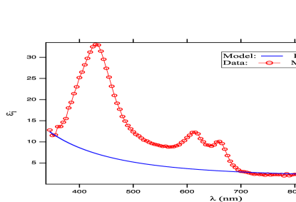
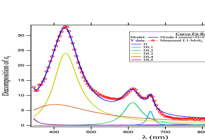
We use the previously discussed models to fit the dynamic values of permittivity available in literature yu and recommend the best fitted permittivity model for MoS2 layers. We consider only the imaginary part of the permittivity as the real part can be estimated using the Kramer-Kronig relation, given by Eq. (4). The formulae for the imaginary part of following Eqs. (19) and (22), are given by
| (25) |
and
| (26) |
in the Drude and DL models, respectively. The values of monolayer MoS2 using Eq. (25) have been graphically presented in Fig. 2. As can be verified from the figure that the Drude model gives accurate permittivity values only in the infrared region and the experimental data disagrees with predictions from Drude model in the visible wavelength (shorter than 700 nm). In this region various interband transitions start contributing. Therefore, it is expected that the DL model will provide a better fit to the measured values. The values using Eq. (26) along with the experimental permittivity values are shown in Fig. 3. It can be noticed from this figure that the measured data from Ref. yu is consistent with the results estimated by the DL model. This suggests that the values estimated using the DL model can be assumed to be reliable for further analysis. The authors in Ref. Mukherjee2015 have used a hybrid Lorentz-Drude-Gaussian (LDG) model in their study to fit the permittivity data for monolayer of MoS2, which is given by
| (27) | |||||
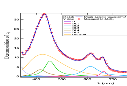
with as mean, as variance and as the maximum amplitude of the Gaussian function. In this case, the term with and carries a weight factor . As seen in Fig.4, by adding a Gaussian background of the above kind with our DL model does not bring much change to our fitted values. Since there is no physical interpretation of the Gaussian component and it is added only as a background to match the estimated values with the experimental results, this justifies our above assertion that the DL model is able to predict permittivity values accurately.
In Tables 3, 4, 5, 6, and 7 we present the fitting values of , , , and from the DL model for various layers of MoS2 along with the uncertainties in them. We use a non-linear least-squares minimization technique to extrapolate the permittivity values at different frequencies and they are decomposed into six components. The first component is named as ‘D’ corresponding to the first term of Eq. (26), whereas the other five components marked as ‘DLj’ corresponding to 1,2,3,4 and 5 in the summation of Eq. (26). We have provided a code written using the python programming language in the Supplementary Material that is used for carrying out this fitting. As can be seen from Table 3, our values for monolayer agree well with those predicted in literature frindt ; eda ; mono1 ; mono2 ; mono3 ; Mukherjee2015 . We also note from these tables that although the uncertainties are quite small for the DL1, DL2, DL3 and DL4 components, they are quite significant for the DL5 and D components. For the DL5 component, only a few data points are available for fitting which lead to significant uncertainties in the fitting parameters corresponding to this component. Also, the inferred value of 27.59 meV for monolayer of MoS2, given in Table 7, matches very well with the measured plasma frequency of 28.3 meV Shen_2013 . We use the fitting value of in Eq. (21) to estimate the effective mass for various number of MoS2 layers. From these calculated values, we further evaluate intrinsic carrier density using the fitting values of in Eq. (20). From Table 7, we also note that is maximum for a monolayer of MoS2, thereafter, it starts decreasing up to layer number 6 and starts increasing again as the number of layers are increased up to 10.
| Layer | Li | Na | K | Rb | Cs |
|---|---|---|---|---|---|
| 1 | 0.879 | 0.960 | 1.455 | 1.613 | 1.932 |
| 2 | 0.810 | 0.883 | 1.340 | 1.484 | 1.776 |
| 3 | 0.784 | 0.853 | 1.296 | 1.434 | 1.716 |
| 4 | 0.766 | 0.833 | 1.266 | 1.401 | 1.677 |
| 5 | 0.752 | 0.817 | 1.243 | 1.374 | 1.645 |
| 6 | 0.752 | 0.818 | 1.243 | 1.375 | 1.645 |
| 7 | 0.839 | 0.917 | 1.388 | 1.540 | 1.845 |
| 8 | 0.853 | 0.933 | 1.413 | 1.567 | 1.878 |
| 9 | 0.860 | 0.940 | 1.424 | 1.580 | 1.893 |
| 10 | 0.866 | 0.948 | 1.435 | 1.592 | 1.908 |

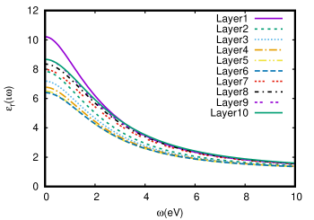
Next, we find values extracted by substituting values in Eq. (4) for different layers of MoS2, which are plotted against frequency in Fig. 5. The behaviour of as a function of layer number is seen to be in accordance with the observation by Yu et al. yu . In their work, the authors demonstrate that excitonic effects play a dominant role in the dielectric function of 5-7 layered MoS2. Therefore, the dielectric function decreases with the layer number up to 6 but turns to increase further with the increase in layer number.
The C3 coefficients for the interactions between Li, Na, K, Rb and Cs atoms and the MoS2 layers evaluated using values are listed in Table 8. A comparison of the C3 coefficient as a function of layer number reveals that the interaction is maximum between atoms and monolayer of MoS2. The interaction decreases with an increase in the number of MoS2 layers up to the sixth layer, then it starts increasing again. The trend is found to be common for all the considered atoms. It is also quite evident that the trend followed by the C3 coefficients with increasing number of layers is similar to that predicted for the intrinsic carrier density . This observation is explained using the fact that the strength of the vdW force depends on the electric polarizability of the interacting atom. The tendency of the MoS2 layer to polarize the incoming atom increases with the increase in the number of electrons per unit volume. As a result, the values of C3 see an upsurge with an escalation in .
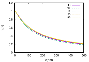
A graphical representation for the C3 coefficients for the considered alkali atoms with varying layer number is shown in Fig. 6. Our results in this figure support the finding that for the same layer number, the C3 coefficients increase with increase in the atomic number. We also notice that the ratio of C3 coefficients among various atoms vary slowly with the number of layers. For instance, the ratio of the C3 coefficient for the interaction of any layer of MoS2 with Rb and Li atoms is 1.83 irrespective of the number of layers. This knowledge of variation pattern of C3 coefficients with number of layers with different alkali atoms will pave way to design sensors for detecting the alkali atoms by the MoS2 layers. To give an estimate of these interactions at an intermediate distance, we next calculate the retardation function as a function of distance for various number of layers in MoS2 based TMDs. We have shown comparison of the values between an atom and the MoS2 monolayer in Fig. 7. It is clear from this figure that the retardation function decreases with increase in . Also, we notice from the above figure that the retardation function is similar for all the considered atoms, and it is not affected much with the atomic size.
VI Conclusion
To summarize, we have investigated the C3 coefficients for the interactions between the alkali atoms with the MoS2 layers. We performed high accuracy calculations of dynamic dipole polarizability of the considered alkali atoms and determined the dynamic dielectric permittivities for different layers of MoS2 over a wide range of imaginary frequency. We have proposed a readily usable logistic fit for the dielectric permittivity for various layers of MoS2 ranging from 1 to 10. We have also shown dependency of the intrinsic carrier density and the coefficients with increasing layer numbers of the MoS2 surface. Variation of C3 as well as with the number of layers shows decrease in values up to 6 number of layers. This finding could be useful for the formation of highly sensitive and reproducible sensing probes for detection of alkali atoms using 1-6 layered MoS2 based transition metal dichalcogenides. Our study reveals that the ratios of the C3 coefficients among various atoms do not change as the layer number is changed.
Acknowledgements.
The work of B.A. is supported by the DST-SERB Grant No. EMR/2016/001228.References
- (1) S. A. Han, R. Bhatia, and S. Kim Nano Convergence, 2, 2015.
- (2) C. Gong et al. Applied Physics Letters, 103:053513, 2013.
- (3) H. Komsa, and A. Krasheninnikov Physical Review B, 88:085318, 2013.
- (4) Prasana Kumar Sahoo et al. ACS Nano, 13(11): 12372–12384, 2019.
- (5) P. K. Sahoo, S. Memaran, Y. Xin, L. Balicas L, H. R. Gutiërrez Nature, 553(7686):63-67, 2018.
- (6) V. O. Özçelik, J. G. Azadani, C. Yang, S. J. Koester and T. Low Physical Review B, 94:035125, 2016.
- (7) F. Withers et al. Nature Materials, 14:301-306, 2015.
- (8) W. Xu et al. Nature, 541:62-67, 2017.
- (9) S. Nakamura et al. Journal of Applied Physics, 34:L797, 1995.
- (10) W. J. Yu et al. Nature Nanotechnology 8:952-958, 2013.
- (11) Y. Zhang et al. IEEE Journal of Quantum Electronics, 47:1475-1479, 2011.
- (12) D. Sarkar et al. Nature 526:91-95, 2015.
- (13) Y. C. Lin et al. Nature Communications 6:7311, 2015.
- (14) S. O. Koswatta, S. J. Koester, and W. Haensch IEEE Transactions on Electronic Devices, 57: 3222-3230, 2010.
- (15) Y. You et al. Nature Physics, 11:477-481, 2015.
- (16) K. He et al. Physical Review Letters, 113:026803, 2014.
- (17) K. F. Mak et al. Nature Physics, 12:207-211, 2012.
- (18) M. Kremser et al. npj 2D materials and Applications, 4, 2020.
- (19) C. E. Stevens et al. Nature Communications, 9:3720, 2018.
- (20) K. Z. Kourosh Q. H. Wan and, A. Kis, J. N. Coleman, and M. S. Strano. Nat. Nanotechnol., 7(699), 2012.
- (21) M. Chhowalla, H. S. Shin, G. Eda, L. J. Li, K. P. Loh, and H. Zhang. Nat. Chem., 5(263), 2013.
- (22) Xiao Li and Hongwei Zhu. Journal of Materiomics, 1(1):33–44, 2015.
- (23) Maurizio Donarelli and Luca Ottaviano. Sensors (Basel, Switzerland), 18(11), 2018.
- (24) Elnaz Akbari, Kia Jahanbin, Abdolkarim Afroozeh, P. Yupapin, and Zolkafle Buntat. Physica B: Condensed Matter, 545(June):510–518, 2018.
- (25) K. F. Mak, C. Lee, J. Hone, J. Shan, and T. F. Heinz. Phys. Rev. Lett., 105(136805), 2010.
- (26) V. Brasch, M. Geiselmann, T. Herr, G. Lihachev, M. H. Pfeiffer, M. L. Gorodetsky, and T. J. Kippenberg. Science, 351(357), 2016.
- (27) Meng Lin Tsai, Sheng Han Su, Jan Kai Chang, Dung Sheng Tsai, Chang Hsiao Chen, Chih I. Wu, Lain Jong Li, Lih Juann Chen, and Jr Hau He. ACS Nano, 8(8):8317–8322, 2014.
- (28) Zongyou Yin, Hai Li, Hong Li, Lin Jiang, Yumeng Shi, Yinghui Sun, Gang Lu, Qing Zhang, Xiaodong Chen, and Hua Zhang. ACS Nano, 6(1):74–80, 2012.
- (29) X. Guo, C.-L. Zou, H. Jung, and H. X. Tang. Phys. Rev. Lett., 117(123902), 2016.
- (30) S. Tongay, J. Zhou, C. Ataca, K. Lo, T. S. Matthews, J. Li, J. C.Grossman, and J. Wu. Nano Lett., 12(5576), 2012.
- (31) H. R. Gutuerrez, N. Perea-Lopez, A. L. Elias, A. Berkdemir, B. Wang, R. L. F. Lopez-Urias, V. H. Crespi, H. Terrones, and M. Terrones. Nano Lett., 13(3447), 2013.
- (32) R. S. Sundaram, M. Engel, A. Lombardo, R. Krupke, A. C. Ferrari, Ph. Avouris, and M. Steiner. Nano Lett., 13(1416), 2013.
- (33) W. Zhao, Z. Ghorannevis, L. Chu, M. Toh, C. Kloc, P. H. Tan, and G. Eda. ACS Nano, 7(791), 2013.
- (34) Unni Krishnan, Manjot Kaur, Kulwinder Singh, Manjeet Kumar, and Akshay Kumar. Superlattices and Microstructures, 128(February):274–297, 2019.
- (35) Zizhen Li, Xiangchao Meng, and Zisheng Zhang. Journal of Photochemistry and Photobiology C: Photochemistry Reviews, 35:39–55, 2018.
- (36) Elton J. G. Santos and Efthimios Kaxiras. ACS Nano, 7(12):10741–10746, 2013. PMID: 24215099.
- (37) W Y Liang. Journal of Physics C: Solid State Physics, 4(18):L378–L381, dec 1971.
- (38) A. R. Beal and H. P. Hughes. Journal of Physics C: Solid State Physics, 12(5):881–890, mar 1979.
- (39) Jiang-Tao Liu, Tong-Biao Wang, Xiao-Jing Li, and Nian-Hua Liu. Journal of Applied Physics, 115(19):193511, 2014.
- (40) S. L. Li, H. Song, H. Kuramochi, S. Nakaharai, and K. Tsukagoshi. ACS Nano, 8:7381, 212.
- (41) A. Castellanos-Gomez, N. Agraït, and G. Rubio-Bollinger. Applied Physics Letters, 96(21):213116, 2010.
- (42) Yiling Yu et al. Scientific Reports, 5, 2015.
- (43) H. Sahin and F. M. Peeters. Phys. Rev. B, 87:085423, Feb 2013.
- (44) Xianlong Wang, Zhi Zeng, Hyojun Ahn, and Guoxiu Wang. Applied Physics Letters, 95(18):183103, 2009.
- (45) Q. Y. He, Z. Y. Lin, Ding MN, et al. Nano Lett., 19:6819–26, 2019.
- (46) Y. Jung, Y. Zhou, J. J. Cha Inorg. Chem. Front., 3:452–63, 2016.
- (47) F. Xiong, H. Wang, X. Liu, et al. Nano Lett., 15:6777–84, 2015.
- (48) J. Xia, J. Wang, D. L. Chao, et al. Nanoscale, 9:7533–40, 2017.
- (49) Y. C. Wang, J. Z. Ou, S. Balendhran, et al. ACS Nano, 7:10083–93, 2013.
- (50) Y. C. Wang, J. Z. Ou, A. F. Chrimes, et al. Nano Lett, 15:883–90, 2015.
- (51) X. D. Li, Y. M. Fang, S. Q. Wu, and Z. Z. Zhu. AIP Advances, 5(5):057143, 2015.
- (52) D. Xiao, G. B. Liu, W. Feng, X. Xu, and W. Yao. Phys. Rev. Lett., 108(196802), 2012.
- (53) C. Ataca and S. Ciraci. J. Phys. Chem. C, 115(13303), 2011.
- (54) J.W. Gadzuk. Theory of atom-metal interactions. Surf. Sci., 6:133–158, 1967.
- (55) E. M. Lifshitz and L. P Pitaevskii. Statistical Physics. Pergamon Press, Oxford, 1980.
- (56) E. M. Lifshitz. Zh. Exsp. Toer. Fiz., 29:94, 1955.
- (57) G. Lach, Maarten Dekieviet, and U. D. Jentschura. Int. J. Mod. Phys. A, 25:2337, 2010.
- (58) Bindiya Arora, Harjeet Kaur, and B. K. Sahoo. J. Phys. B: At. Mol. Opt. Phys., 47:155002, 2014.
- (59) Bindiya Arora and B. K. Sahoo. Phys. Rev. A, 86:033416, 2012.
- (60) D B Melrose and R J Stoneham. J. Phys. A: Math. Gen., 1977.
- (61) P. Kharchenko, J. F. Babb, and A. Dalgarno. Phys. Rev. A, 55:3566, 1997.
- (62) Jasmeet Kaur, D. K. Nandy, Bindiya Arora, and B. K. Sahoo. Phys. Rev. A, 91:012705, 2015.
- (63) Bindiya Arora, D. K. Nandy, and B. K. Sahoo. Phys. Rev. A, 85:012506, 2012.
- (64) Bindiya Arora, D. K. Nandy, and B. K. Sahoo. Phys. Rev. A, 85:012506, 2012.
- (65) A. Derevianko, W. R. Johnson, M. S. Safronova, and J. F. Babb. Phys. Rev. Lett., 82:3589, 1999.
- (66) Bindiya Arora, M. S. Safronova, and Charles W. Clark. Phys. Rev. A, 76:052509, 2007.
- (67) Sergey G. Porsev and Andrei Derevianko. J. Chem. Phys., 119:844, 2003.
- (68) B. K. Sahoo and Bindiya Arora. Phys. Rev. A, 87:023402, 2013.
- (69) Bindiya Arora and B.K. Sahoo. Phys. Rev. A, 89(022511), 2014.
- (70) Y. Singh and B. K. Sahoo. Phys. Rev. A, 90:022511, 2014.
- (71) D. Mukherjee and S. Pal. Adv. Quant. Chem., 20:281, 1989.
- (72) B. K. Sahoo. J. Phys. B, 43:085005, 2010.
- (73) B. K. Sahoo, T. Aoki, B. P. Das, and Y. Sakemi. Phys. Rev. A, 93:032520, 2016.
- (74) B. K. Sahoo, D. K. Nandy, B. P. Das, and Y. Sakemi. Phys. Rev. A, 91:042507, 2015.
- (75) B. K. Sahoo and B. P. Das. Phys.Rev. A, 92:052511, 2015.
- (76) B. K. Sahoo. Phys. Rev. A, 92:052506, 2015.
- (77) Vita Efelina, Eri Widianto, Kiki Megasari, Kuwat Triyana, Ahmad Kusumaatmaja, Andrivo Rusydi, and Iman Santoso. AIP Conference Proceedings, 1755:150008, 2016.
- (78) B. Mukherjee, F. Tseng, D. Gunlycke, K. K. Amara, G. Eda, , and E. Simsek. Optical Materials Express, 5:447–455, 2015.
- (79) W. Cai and V. M. Shalaev. Optical Metamaterials: Fundamentals and Applications. Springer, New York, 2010.
- (80) Xianding Yan, Lipeng Zhu, Yixuan Zhou, Yiwen E, Li Wang, and Xinlong Xu. Appl. Opt., 54(22):6732–6736, Aug 2015.
- (81) A. Miffre, M. Jacquest, M. Buchner, G. Trenec, and J. Vigue. Eur. Phys. J. D, 38:353, 2006.
- (82) William F. Holmgren, Melissa C. Revelle, Vincent P. A. Lonij, and Alexander D. Cronin. Phys. Rev. A, 81:053607, May 2010.
- (83) M. D. Gregoireand Nathan Brooks, Raisa Trubko, and A. D. Cronin. Atoms, 4:3, 2016.
- (84) Chih-Chiang Shen, Yu-Te Hsu, Lain-Jong Li, and Hsiang-Lin Liu. Applied Physics Express, 6(12):125801, dec 2013.
- (85) R. F. Frindt and A. D. Yoffe. Proc. R. Soc. Lond. A, 273:135269, 1963.
- (86) G. Eda, H. Yamaguchi, T. Fujita D. Voiry, M. Chen, and M. Chhowallam. Nano Lett., 11:5111, 2011.
- (87) T. Cheiwchanchamnangij and W. R. Lambrecht. Phys. Rev. B, 85:205302, 2012.
- (88) A. Ramasubramaniam. Phys. Rev. B, 86:115409, 2012.
- (89) D.Y.Qiu, F.H. da Jornada, and S.G.Louie. Phys. Rev. Lett., 111:216805, 2013.