Efficiently-coupled microring circuit for on-chip cavity QED with trapped atoms
Abstract
We present a complete fabrication study of an efficiently-coupled microring optical circuit tailored for cavity quantum electrodynamics (QED) with trapped atoms. The microring structures are fabricated on a transparent membrane with high in-vacuum fiber edge-coupling efficiency in a broad frequency band. In addition, a bus waveguide pulley coupler realizes critical coupling to the microrings at both of the cesium D-line frequencies, while high coupling efficiency is achieved at the cesium ‘magic’ wavelengths for creating a lattice of two-color evanescent field traps above a microring. The presented platform holds promises for realizing a robust atom-nanophotonics hybrid quantum device.
Cold atoms trapped and interfaced with light in photonic optical circuits form exciting hybrid quantum platforms for quantum optics and atomic physics. Strong optical confinement in nanophotonic waveguides or resonators greatly enhances atom-light coupling beyond those achieved in diffraction-limited optics, enabling opportunities in studying light-matter interactions [1, 2, 3, 4, 5, 6, 7, 8] and radiative processes [9, 10, 11]. On the circuit-level, nanophotonic engineering offers a variety of tools in modifying the photonic density of states [12, 13], as well as controlling photon transport and device optical links [14, 15, 16, 17, 18], thus enriching the complexity of atom-photon interactions and quantum functionality. The indistinguishability and long coherence time of neutral atoms make an atom-nanophotonic hybrid platform inherently scalable, and by itself a strongly coupled many-body system [19, 20, 13]. Recent developments in suspended photonic crystal waveguides and microring resonators [21, 22, 23, 24, 8] hold great promises in realizing highly coherent quantum circuits with cold atoms in cavity QED and waveguide QED settings [13].
Engineering an integrated photonic circuit that fulfills all technical requirements has so-far remained a challenging task. Ideally, the circuit geometry should be compatible with atom cooling and trapping. Nanophotonic waveguides and resonators must be fabricated with high precision, and offer sufficient tunability for alignment with narrow atomic spectral lines. To perform quantum operations with high fidelity, photons should be coupled into and out of a circuit with high efficiency. It is advantageous that a photonic nanostructure could also be utilized to create far off-resonant optical traps to localize cold atoms[25, 26]. Taking cesium atoms for example, a two-color evanescent field trap formed using the ‘magic’ wavelengths (794 nm and 935 nm) can create a better trap for coherent quantum operations [27, 28]. As such, all coupling elements to the circuit should work in a broad frequency band.
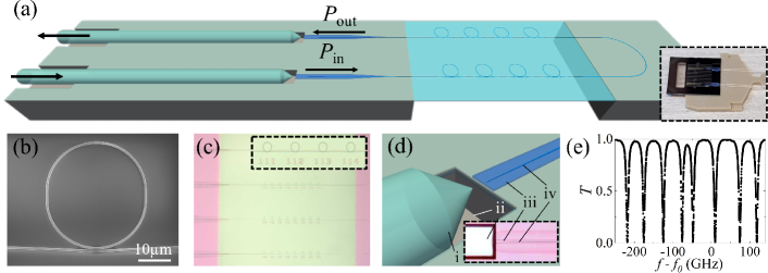
In the letter, we discuss design and full fabrication procedures of an efficiently-coupled microring optical circuit that meets the above key requirements for building a robust hybrid quantum device. An overview of our platform is shown in Fig. 1, where Si3N4 microring resonators are evanescently coupled to a bus waveguide in a pulley geometry for optical input and output [Fig. 1(b-c)]. The microrings are top vacuum-cladded and are fabricated on a transparent SiO2-Si3N4 double-layer membrane (Fig. 1(c) and Fig. 2), suspended over a large window (2 mm8 mm) on a silicon chip. This ensures full optical access for laser cooling and cold atom trapping [29]. The microring geometry is designed to optimize the cooperativity parameter for cavity QED with cesium atoms [23], where nm ( nm) is the wavelength of Cs D1 (D2) line. The microring radius is m and the waveguide width and height are nm, respectively (Fig. 2). A nearly optimal ratio is achieved, giving with an intrinsic quality factor , currently limited by the surface scattering loss[23], and a mode volume m3, evaluated using the normalized transverse-magnetic (TM) mode field amplitude at an atomic position nm centered above the microring dielectric surface. We adopt the fundamental TM-mode for its uniform polarization above a microring [23].
By lithographically scanning the length of each microring (Fig. 1(b)), their resonances approach the targeted frequency as shown in the transmission spectrum in Fig. 1(e). Precise alignment to the atomic spectral lines can be thermally tuned, for example, by a laser beam globally heating the silicon substrate under vacuum. The tunability is GHz/mW. The transmission spectrum is measured through lensed fibers coupled to either end of the bus waveguide via an edge-coupler (Fig. 1(d)). Each of the resonances in Fig. 1(e) displays nearly zero transmission , achieving the ideal critical coupling condition for probing atom-microring coupling; see Fig. 4.
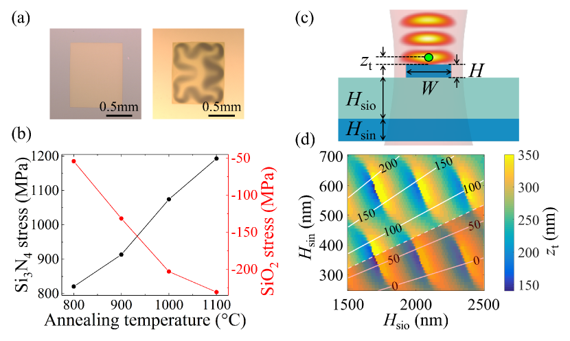
We begin the circuit fabrication by preparing for a SiO2-Si3N4 double-layer membrane stack, deposited on a silicon wafer using low-pressure chemical vapor deposition (LPCVD) processes. For stable membrane release from the silicon substrate, the compressive stress of the SiO2 layer (m thick) should be overcome by the tensile stress of the Si3N4 bottom-layer, giving a thickness-weighted tensile resulting stress [30]. We arrive at a proper stress condition by post-annealing at around C for the Si3N4 bottom-layer and at C after we deposited the SiO2 layer, two hours for each time (Fig. 2(b)). In our results, a post-annealed membrane can be released free from buckling and severe cracking under a tensile stress of MPa.
Optical reflectance is another crucial factor in determining the membrane thickness, primarily concerning atom trapping. For example, in a top-illuminating optical tweezer trap implemented in Ref. [29] or [31], membrane reflection and interference result in a lattice of micro traps formed within a tweezer beam as shown in Fig. 2(c). We scan the SiO2/Si3N4 layer thickness to minimize the position of the first micro trap (formed by an anti-node) in a tweezer potential, while monitoring the resulting stress. An example is shown in Fig. 2(d), calculated for a 935 nm tweezer trap focused by an objective of numerical aperture N.A.. A micro trap at nm forms with layer thickness m within the stable membrane regime.
Once the membrane stack is fabricated, an additional LPCVD-grown Si3N4 top-layer is deposited, and the wafer is diced into centimeter-sized chips (Fig. 1(a) inset). Microring arrays and bus waveguides are then fabricated in the top layer using e-beam lithography with multipass writing and an inductively coupled plasma reactive-ion etching (ICP-RIE) process with CHF3/O2 gas chemistry [32].
Either end of a bus waveguide is designed to taper down and terminate at a width of 70 nm for edge-coupling with a lensed fiber [33] (1 m focused beam waist), which is placed inside a U-shaped fiber groove of m depth (Fig. 1(d)). To achieve high coupling efficiency, a top-cladding structure on each edge-coupler is designed to improve symmetric mode matching with the lensed fiber. The geometry of the top-cladded edge-coupler has been numerically optimized using finite-different-time-domain calculations to achieve 70% coupling efficiency at Cs D-lines. The same coupler yields an efficiency 70% (60%) at 935 nm (794 nm).
To fabricate the top-cladding structure on each edge-coupler defined in the first lithography step, we cover the tapered bus waveguides with 1 m-thick hydrogen silsesquioxane (HSQ) resist as the top-cladding material. Using second e-beam lithography, we define the top-cladding structures to inversely taper down along the bus waveguides (Fig. 1(d)) so to keep the microrings top vacuum-cladded. Fiber grooves and edge-coupler facets are defined in a subsequent photolithography step. HSQ and SiO2 are then etched away in the ICP-RIE, followed by the Bosch process etching to create fiber U-grooves in the silicon.
Following the fabrication of photonic structures at the front side of the chip, the membrane is then released from the silicon substrate. To do this, a window at the backside of the chip is first defined using photolithography, while the front-side is protected with a thick layer of spin-coated photoresist (PMMA 950 coating with Surpass 3000 adhesion promoter). Materials at the backside are etched away in the ICP-RIE and the Bosch process until leftover silicon is only m thick. To gently release the membrane, we perform wet-etching in a 12% aqueous TMAH solution at 65 °C, followed by DI water rinsing and cleaning with PRS-2000 stripper and Nanostrip to expose the front-side photonic structures. Finally, a thin alumina layer (nm) is deposited using atomic layer deposition to protect the microrings against cesium corrosion during experiments [34].
Our fabrication procedure yields nearly 100% success rate on membrane release. The released membrane is optically flat and has a root-mean-squared surface roughness of nm. Additional chemical mechanical polishing step [32] can be applied to the SiO2-Si3N4 double-layer stack following LPCVD. We have measured surface roughness down below nm, which is expected to improve the microring quality factor to using similar fabrication procedures [23].
In the final step, optical lensed fibers are introduced to the fiber grooves. The alignment tolerance is m for 1-dB excess loss. Fine adjustment in the U-groove is required prior to epoxy fixture. We note that misalignment can occur under vacuum when bulk epoxy outgases and shrinks. Therefore, only a thin layer of low viscosity UV epoxy (OG198-54) is applied for alignment fixture. We achieve 50% (3dB loss) coupling efficiency per facet, which persists under vacuum pressure below Torr. The fibers are guided out of a vacuum chamber without noticeable loss via a teflon feedthrough mounted on a Swagelok fitting [35].
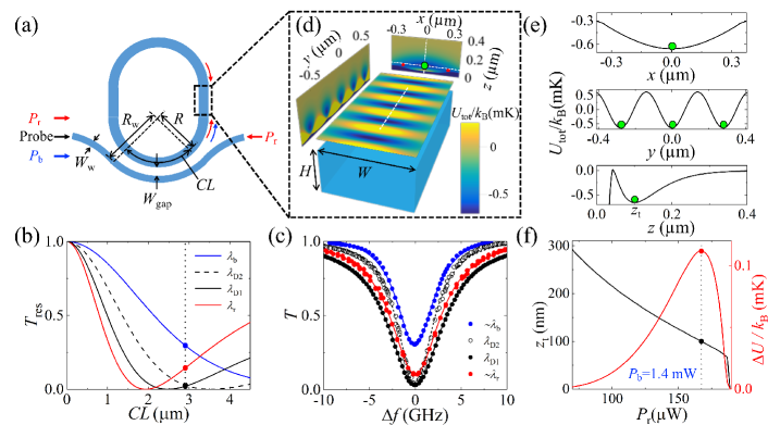
We now discuss the design of pulley couplers (Fig. 3(a)), which allows us to separately optimize the bus waveguide parameters and the coupling length for efficient microring coupling over a wide frequency band. We perform a finite element method (FEM) analysis to calculate the microring coupling rate [36] , where is the normalized sinc function, is the coupling wavelength ( is the angular frequency), , and the integration runs over the cross-section of the bus waveguide with being its dielectric function; correspond to the normalized resonator (bus waveguide) mode field, the effective refractive index, and the bend radius, respectively. By comparing with the microring intrinsic decay rate , also evaluated using a FEM analysis [23], we can optimize the bus waveguide-microring coupling efficiency numerically.
Figure 3(b) shows the expected resonant transmission as a function of the coupling length . The better the coupling efficiency, the lower the transmission. Approaching the critical coupling condition (), all of the resonant input photons can be drawn into the microring, hence, resulting in zero transmission . In this calculation, the pulley coupler geometry is chosen to improve the overlap of the critical coupling regions () of all four relevant wavelengths. For the fabricated devices, we have selected m to approach critical coupling for Cs D-lines at and , respectively, while maintaining sufficient coupling efficiency near and magic wavelengths for two-color evanescent field traps [23]. We anticipate for test wavelengths nm, respectively, which are in very good agreement with the measurement as shown in Fig. 3 (c).
The agreement between the bus waveguide transmission measurement and full simulation results illustrate the fabrication precision of our microring optical circuit. Meanwhile, the absence of resonance splitting in the transmission data (Fig. 3 (c)) suggests that there is negligible mode-mixing caused by coherent back-scattering in the microring resonator [23, 37]. Therefore, the resonant TM modes preserve the traveling-wave characteristics of a whispering-gallery mode (WGM) [23].
Combining our measurement and FEM simulation results, we can now estimate the actual power required to create a stable two-color evanescent field trap. One sample scheme is illustrated in Fig. 3 (a). A resonant TM mode near the wavelength is excited from the bus waveguide to create a smooth and short-range repulsive optical potential, preventing atoms from crashing onto the microring surface. Additional two phase-coherent, counter-propagating TM modes near the wavelength are excited from either end of the bus waveguide to create an attractive optical lattice-like potential, localizing atoms tightly above the microring. We note that, given the finite free spectral range of the microring, to achieve a satisfactory alignment of the microring resonances near the Cs magic wavelengths while maintaining the exact alignment of a resonator mode to the Cs D-line (through thermal tuning) requires further lithographic-tuning of the microring geometrical parameters near the reported values. Fig. 3 (d-e) plot the total ground state trap potential , including the direct summation of repulsive and attractive potentials calculated using the electric field profiles obtained from the FEM analyses and the build-up intensity in the microring with a total input power of mW. We have also added in an approximate Casimir-Polder attractive potential , where Hzm4 is the Cs-Si3N4 surface interaction coefficient and nm is an effective wavelength [38].
The two-color evanescent field trap is robust and tunable. The vertical trap location and the trap depth can be finely controlled by the power of injected light (Fig. 3(f)). At an optimal power ratio shown in Fig. 3(e), the trap can be tuned to nm with K, much deeper than the thermal energy K of polarization-gradient cooled cesium atoms, where is the Boltzmann constant.
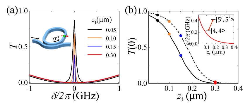
By realizing atom trapping and a critically-coupled microring resonator aligned to an atomic resonance, it is possible to probe the interaction between single atoms and resonator photons with high sensitivity. As a simple example, in Fig. 4 we plot a weakly-driven, steady-state bus waveguide transmission [39, 11], , where is the laser detuning from the atomic resonance (D2 line), is the position-dependent atom-photon coupling strength (Fig. 4(b) inset), MHz is the atomic decay rate, and the resonator decay rate GHz is extracted from the measurement. A trapped atom is assumed to be initially polarized in the ground state and is excited to by a circularly polarized counter-clockwise (CCW) circulating WGM as shown in Fig. 4(a) inset. Significant increase in the bus waveguide transmission can be observed near the atomic resonance when . This transparency window results from the destructive interference between atom-WGM photon dressed states, similar to the electromagnetically-induced transparency effect [40, 41, 42]. At the desired trap location nm, we expect MHz and ( for currently best available GHz), which greatly contrasts of an empty microring (Fig. 4(b)). The large variation of bus waveguide transmission could thus inform us the presence of single atom and the strength of atom-photon coupling with high sensitivity [39, 43]. Lastly, we note that the WGM circular polarization results from strong confinement in the microring nanowaveguide; the polarization is locked to the direction of the WGM circulation [44]. Creating a directional coupling with spin-polarized atoms can give rise to applications, for example, in chiral quantum optics [4, 6, 45].
We demonstrate a microring optical circuit that permits precision understanding of fabrication performance and analyses of the optical modes. Our circuit is efficiently coupled, scalable, and can simultaneously accommodate large number of atoms trapped in an array of surface micro traps. With near-term improvement on the membrane surface quality[23] and reduction of other surface scattering sources[32, 46], one expects more than ten-fold increase in the quality factor to achieve large cooperativity when the microring is critically coupled. Coherent quantum operations with a single atom or in a hybrid lattice formed by atoms and photons can be realized following introduction of cold atoms to the microring to form a hybrid quantum circuit with strong atom-photon interactions. In the latter case, the hybrid lattice can form a strongly coupled many-body system with WGM photon-mediated interaction among all trapped atoms [19]. Non-uniform or pair-wise tunable interactions can be achieved in this resonator by using local addressing, via top-projected optical tweezers, or a multi-frequency pumping scheme as detailed in Ref. [20]. Dynamics of the strongly-coupled hybrid lattice may be probed via the efficiently coupled bus waveguide, or by using single atom-resolved fluorescence imaging [29, 47].
Funding is provided by the AFOSR YIP (Grant NO. FA9550-17-1-0298) and the ONR (Grant NO. N00014-17-1-2289). X. Zhou and M. Zhu acknowledge support from the Rolf Scharenberg Graduate Fellowship. The data that support the findings of this study are available from the corresponding author upon reasonable request.
References
- Thompson et al. [2013] J. D. Thompson, T. G. Tiecke, N. P. de Leon, J. Feist, A. V. Akimov, M. Gullans, A. S. Zibrov, V. Vuletić, and M. D. Lukin, “Coupling a single trapped atom to a nanoscale optical cavity,” Science 340, 1202–1205 (2013).
- Tiecke et al. [2014] T. G. Tiecke, J. D. Thompson, N. P. de Leon, L. R. Liu, V. Vuletić, and M. D. Lukin, “Nanophotonic quantum phase switch with a single atom,” Nature 508, 241–244 (2014).
- Goban et al. [2014] A. Goban, C.-L. Hung, S.-P. Yu, J. D. Hood, J. A. Muniz, J. H. Lee, M. J. Martin, A. C. McClung, K. S. Choi, D. E. Chang, O. Painter, and H. J. Kimble, “Atom–light interactions in photonic crystals,” Nature Communications 5, 3808 (2014).
- Mitsch et al. [2014] R. Mitsch, C. Sayrin, B. Albrecht, P. Schneeweiss, and A. Rauschenbeutel, “Quantum state-controlled directional spontaneous emission of photons into a nanophotonic waveguide,” Nature Communications 5, 5713 (2014).
- Goban et al. [2015] A. Goban, C.-L. Hung, J. D. Hood, S.-P. Yu, J. A. Muniz, O. Painter, and H. J. Kimble, “Superradiance for atoms trapped along a photonic crystal waveguide,” Phys. Rev. Lett. 115, 063601 (2015).
- Scheucher et al. [2016] M. Scheucher, A. Hilico, E. Will, J. Volz, and A. Rauschenbeutel, “Quantum optical circulator controlled by a single chirally coupled atom,” Science 354, 1577–1580 (2016).
- Corzo et al. [2019] N. V. Corzo, J. Raskop, A. Chandra, A. S. Sheremet, B. Gouraud, and J. Laurat, “Waveguide-coupled single collective excitation of atomic arrays,” Nature 566, 359–362 (2019).
- Samutpraphoot et al. [2020] P. Samutpraphoot, T. Đorđević, P. L. Ocola, H. Bernien, C. Senko, V. Vuletić, and M. D. Lukin, “Strong coupling of two individually controlled atoms via a nanophotonic cavity,” Phys. Rev. Lett. 124, 063602 (2020).
- Perez-Rios, Kim, and Hung [2017] J. Perez-Rios, M. E. Kim, and C.-L. Hung, “Ultracold molecule assembly with photonic crystals,” New Journal of Physics 19, 123035 (2017).
- Grandi et al. [2019] S. Grandi, M. P. Nielsen, J. Cambiasso, S. Boissier, K. D. Major, C. Reardon, T. F. Krauss, R. F. Oulton, E. Hinds, and A. S. Clark, “Hybrid plasmonic waveguide coupling of photons from a single molecule,” APL Photonics 4, 086101 (2019).
- Zhu, Wei, and Hung [2020] M. Zhu, Y.-C. Wei, and C.-L. Hung, “Resonator-assisted single-molecule quantum state detection,” Phys. Rev. A 102, 023716 (2020).
- Joannopoulos et al. [2008] J. D. Joannopoulos, S. G. Johnson, J. N. Winn, and R. D. Meade, Photonic Crystals: Molding the Flow of Light, 2nd ed. (Princeton University Press, 2008).
- Chang et al. [2018] D. E. Chang, J. S. Douglas, A. González-Tudela, C.-L. Hung, and H. J. Kimble, “Colloquium: Quantum matter built from nanoscopic lattices of atoms and photons,” Rev. Mod. Phys. 90, 031002 (2018).
- Hafezi et al. [2013] M. Hafezi, S. Mittal, J. Fan, A. Migdall, and J. Taylor, “Imaging topological edge states in silicon photonics,” Nature Photonics 7, 1001–1005 (2013).
- Ozawa et al. [2019] T. Ozawa, H. M. Price, A. Amo, N. Goldman, M. Hafezi, L. Lu, M. C. Rechtsman, D. Schuster, J. Simon, O. Zilberberg, et al., “Topological photonics,” Reviews of Modern Physics 91, 015006 (2019).
- Elshaari et al. [2020] A. W. Elshaari, W. Pernice, K. Srinivasan, O. Benson, and V. Zwiller, “Hybrid integrated quantum photonic circuits,” Nature Photonics , 1–14 (2020).
- Stern et al. [2013] L. Stern, B. Desiatov, I. Goykhman, and U. Levy, “Nanoscale light–matter interactions in atomic cladding waveguides,” Nature communications 4, 1–7 (2013).
- Solano et al. [2017] P. Solano, P. Barberis-Blostein, F. K. Fatemi, L. A. Orozco, and S. L. Rolston, “Super-radiance reveals infinite-range dipole interactions through a nanofiber,” Nature communications 8, 1–7 (2017).
- Douglas et al. [2015] J. S. Douglas, H. Habibian, C.-L. Hung, A. V. Gorshkov, H. J. Kimble, and D. E. Chang, “Quantum many-body models with cold atoms coupled to photonic crystals,” Nature Photonics 9, 326–331 (2015).
- Hung et al. [2016] C.-L. Hung, A. González-Tudela, J. I. Cirac, and H. J. Kimble, “Quantum spin dynamics with pairwise-tunable, long-range interactions,” Proceedings of the National Academy of Sciences 113, E4946–E4955 (2016).
- Yu et al. [2014] S.-P. Yu, J. D. Hood, J. A. Muniz, M. J. Martin, R. Norte, C.-L. Hung, S. M. Meenehan, J. D. Cohen, O. Painter, and H. J. Kimble, “Nanowire photonic crystal waveguides for single-atom trapping and strong light-matter interactions,” Applied Physics Letters 104, 111103 (2014).
- Yu et al. [2019] S.-P. Yu, J. A. Muniz, C.-L. Hung, and H. Kimble, “Two-dimensional photonic crystals for engineering atom–light interactions,” Proceedings of the National Academy of Sciences 116, 12743–12751 (2019).
- Chang et al. [2019] T.-H. Chang, B. M. Fields, M. E. Kim, and C.-L. Hung, “Microring resonators on a suspended membrane circuit for atom-light interactions,” Optica 6, 1203–1210 (2019).
- Luan et al. [2020] X. Luan, J.-B. Béguin, A. P. Burgers, Z. Qin, S.-P. Yu, and H. J. Kimble, “The integration of photonic crystal waveguides with atom arrays in optical tweezers,” Advanced Quantum Technologies , 2000008 (2020).
- Le Kien, Balykin, and Hakuta [2004] F. Le Kien, V. I. Balykin, and K. Hakuta, “Atom trap and waveguide using a two-color evanescent light field around a subwavelength-diameter optical fiber,” Phys. Rev. A 70, 063403 (2004).
- Vetsch et al. [2010] E. Vetsch, D. Reitz, G. Sagué, R. Schmidt, S. T. Dawkins, and A. Rauschenbeutel, “Optical interface created by laser-cooled atoms trapped in the evanescent field surrounding an optical nanofiber,” Phys. Rev. Lett. 104, 203603 (2010).
- Goban et al. [2012] A. Goban, K. S. Choi, D. J. Alton, D. Ding, C. Lacroûte, M. Pototschnig, T. Thiele, N. P. Stern, and H. J. Kimble, “Demonstration of a state-insensitive, compensated nanofiber trap,” Phys. Rev. Lett. 109, 033603 (2012).
- Hung et al. [2013] C.-L. Hung, S. M. Meenehan, D. E. Chang, O. Painter, and H. J. Kimble, “Trapped atoms in one-dimensional photonic crystals,” New Journal of Physics 15, 083026 (2013).
- Kim et al. [2019] M. E. Kim, T.-H. Chang, B. M. Fields, C.-A. Chen, and C.-L. Hung, “Trapping single atoms on a nanophotonic circuit with configurable tweezer lattices,” Nature Communications 10, 1647 (2019).
- Rossi, Temple-Boyer, and Estève [1998] C. Rossi, P. Temple-Boyer, and D. Estève, “Realization and performance of thin sio2/sinx membrane for microheater applications,” Sensors and Actuators A: Physical 64, 241–245 (1998).
- Béguin et al. [2020] J. B. Béguin, J. Laurat, X. Luan, A. P. Burgers, Z. Qin, and H. J. Kimble, “Reduced volume and reflection for optical tweezers with radial laguerre-gauss beams,” (2020), arXiv:2001.11498 [quant-ph] .
- Ji et al. [2017] X. Ji, F. A. S. Barbosa, S. P. Roberts, A. Dutt, J. Cardenas, Y. Okawachi, A. Bryant, A. L. Gaeta, and M. Lipson, “Ultra-low-loss on-chip resonators with sub-milliwatt parametric oscillation threshold,” Optica 4, 619–624 (2017).
- Cardenas et al. [2014] J. Cardenas, C. B. Poitras, K. Luke, L. Luo, P. A. Morton, and M. Lipson, “High coupling efficiency etched facet tapers in silicon waveguides,” IEEE Photonics Technology Letters 26, 2380–2382 (2014).
- Woetzel et al. [2013] S. Woetzel, F. Talkenberg, T. Scholtes, R. Ijsselsteijn, V. Schultze, and H.-G. Meyer, “Lifetime improvement of micro-fabricated alkali vapor cells by atomic layer deposited wall coatings,” Surface and Coatings Technology 221, 158–162 (2013).
- Abraham and Cornell [1998] E. R. Abraham and E. A. Cornell, “Teflon feedthrough for coupling optical fibers into ultrahigh vacuum systems,” Applied optics 37, 1762–1763 (1998).
- Hosseini et al. [2010] E. S. Hosseini, S. Yegnanarayanan, A. H. Atabaki, M. Soltani, and A. Adibi, “Systematic design and fabrication of high-q single-mode pulley-coupled planar silicon nitride microdisk resonators at visible wavelengths,” Opt. Express 18, 2127–2136 (2010).
- Srinivasan and Painter [2007] K. Srinivasan and O. Painter, “Mode coupling and cavity–quantum-dot interactions in a fiber-coupled microdisk cavity,” Phys. Rev. A 75, 023814 (2007).
- Stern, Alton, and Kimble [2011] N. P. Stern, D. J. Alton, and H. J. Kimble, “Simulations of atomic trajectories near a dielectric surface,” New Journal of Physics 13, 085004 (2011).
- Aoki et al. [2006] T. Aoki, B. Dayan, E. Wilcut, W. P. Bowen, A. S. Parkins, T. Kippenberg, K. Vahala, and H. Kimble, “Observation of strong coupling between one atom and a monolithic microresonator,” Nature 443, 671–674 (2006).
- Junge et al. [2013] C. Junge, D. O’Shea, J. Volz, and A. Rauschenbeutel, “Strong coupling between single atoms and nontransversal photons,” Phys. Rev. Lett. 110, 213604 (2013).
- Tanji-Suzuki et al. [2011] H. Tanji-Suzuki, W. Chen, R. Landig, J. Simon, and V. Vuletić, “Vacuum-induced transparency,” Science 333, 1266–1269 (2011).
- Mücke et al. [2010] M. Mücke, E. Figueroa, J. Bochmann, C. Hahn, K. Murr, S. Ritter, C. J. Villas-Boas, and G. Rempe, “Electromagnetically induced transparency with single atoms in a cavity,” Nature 465, 755–758 (2010).
- Shomroni et al. [2014] I. Shomroni, S. Rosenblum, Y. Lovsky, O. Bechler, G. Guendelman, and B. Dayan, “All-optical routing of single photons by a one-atom switch controlled by a single photon,” Science 345, 903–906 (2014).
- Mechelen and Jacob [2016] T. V. Mechelen and Z. Jacob, “Universal spin-momentum locking of evanescent waves,” Optica 3, 118–126 (2016).
- Lodahl et al. [2017] P. Lodahl, S. Mahmoodian, S. Stobbe, A. Rauschenbeutel, P. Schneeweiss, J. Volz, H. Pichler, and P. Zoller, “Chiral quantum optics,” Nature 541, 473–480 (2017).
- Porkolab et al. [2014] G. A. Porkolab, P. Apiratikul, B. Wang, S. H. Guo, and C. J. K. Richardson, “Low propagation loss algaas waveguides fabricated with plasma-assisted photoresist reflow,” Opt. Express 22, 7733–7743 (2014).
- Meng et al. [2020] Y. Meng, C. Liedl, S. Pucher, A. Rauschenbeutel, and P. Schneeweiss, “Imaging and localizing individual atoms interfaced with a nanophotonic waveguide,” Phys. Rev. Lett. 125, 053603 (2020).