Largely enhanced photogalvanic effects in the phosphorene photodetector by strain-increased device asymmetry
Abstract
Photogalvanic effect (PGE) occurring in noncentrosymmetric materials enables the generation of the open-circuit voltage that is much larger than the bandgap, making it rather attractive in solar cells. However, the magnitude of the PGE photocurrent is usually small, which severely hampers its practical application. Here we propose a mechanism to largely enhance the PGE photocurrent by mechanical strain based on the quantum transport simulations for the two-dimensional nickel-phosphorene-nickel photodetector. Broadband PGE photocurrent governed by the noncentrosymmetry is generated at zero bias under the illumination of linearly polarized light. The photocurrent depends linearly on the device asymmetry, while nonlinearly on the optical absorption. By applying the appropriate mechanical tension stress on the phosphorene, the photocurrent can be substantially enhanced by up to 3 orders of magnitude, which is primarily ascribed to the largely increased device asymmetry. The change in the optical absorption in some cases can also play a critical role in tuning the photocurrent due to the nonlinear dependence. Moreover, the photocurrent can even be further enhanced by the mechanical bending, mainly owing to the considerably enhanced device asymmetry. Our results reveal the dependence of the PGE photocurrent on the device asymmetry and absorption in transport process through a device, and also explore the potentials of the PGE in the self-powered low-dimensional flexible optoelectronics, and low-dimensional photodetections with high photoresponsivity.
I INTRODUCTION
Optoelectronic properties of the two dimensional (2D) materials have attracted intensive research interest in the past decades for their fascinating potential applications in various fields including photodetections,AFM2019-29-1803807 ; AM201830-1801164 ; APR2019 ; APR2019b ; ACSNano.2019.13.9907 solar cellsNat.2019 ; Science.2018.360 and spintronics.NC2019-10-3965 ; PNAS2016-113-3746 ; PRA2018 There are several light-to-current conversion mechanisms that are usually involved in these 2D optoelectronic devices. The most typical mechanism is the photovoltaic effect which requires the traditional - junctions to separate the light induced electron-holes. Their efficiency has been improved largely in these years and almost reaches the Shockley-Queisser limitation.Shockley The second one is the photoconductor effect, in which the external voltage is necessary for generating the persistent current, yet can not provide the electrical power generation.huang2016highly ; furchi2014mechanisms Other mechanisms like photo-gating effects are also involved.wang2014inkjet ; qian2017high ; cao2019enhanced
In contrast to these light-to-current conversion mechanisms, the photogalvanic effect (PGE),Sov.Phys.Usp.23.199 ; APL.2002.77.3146 ; PgeJPCM.2003.15.20 ; nanoscale ; xiePRA ; ACS2020 also known as the bulk photovoltaic effect (BPVE),PRB.23.5590 ; APL ; Sci.Adv.2019.5 enables the generation of the photocurrent without the need of any external voltage or the - junctions, which occurs in materials with broken inversion symmetry. The PGE has attracted a broad researching interest in wide material systems, including the bulk Weyl semimetals,Nat.Mater.2019.18.9 ; Nat.Mater.2019.18.5 quantum wells,APL.2002.77.3146 and 2D materials.nat.Commun.2018.9 This mechanism is able to generate an open-circuit voltage that is much larger than the bandgap,APL ; Nat.Commun.8.281-2017 which makes it possible to achieve the light-to-current efficiency exceeding the Shockley-Queisser limit.Nat.Photonics.2016.10.9 However, high efficiency has been hardly achieved so far in experiments mainly because of the low magnitude of the PGE photocurrent (photoresponsivity) which is usually less than mA/W. It is therefore rather desirable to find an effective approach to enhance the PGE photocurrent.
Breakthroughs have been achieved recently. It has been demonstrated that the PGE photocurrent obtained in the 1D WS2 nanotubes is several orders of magnitude larger than that in the flat 2D WS2 mono-layers,Nat.2019 and the photoresponsivity is of up to 0.1 A/W, which is much larger than those PGE ever reported in other systems, such as the bulk BaTiO3Nat.Photonics.2016.10.9 , TTF-CAdressel2017infrared and organometallic perovskite halideAPL.2016.109 . This substantially enhanced photocurrent in the 1D WS2 nanotube has been mainly ascribed to its reduced or symmetry, as compared to the 2D WS2 monolayer (), along with the increased optical absorption. These results suggested that reducing the crystal symmetry of a flat 2D semiconducting material by creating a curvature (e.g., bending) can strengthen the PGE and hence enhance the photocurrent. Another important experiment has demonstrated that by applying appropriate mechanical stress gradient on the SrTiO3 single crystal the PGE photocurrent can be enhanced by orders of magnitude,Science.2018.360 which is known as the flexo-photovoltaic effect. However, controversy has been raised regarding the fundamental mechanism responsible for this enhancement in photocurrent.ACSNano.2019.13.12259 A direct experimental evidence for the effective enhancement of the PGE by mechanical strain has been achieved recently in the Fe-doped LiNbO3 single crystal, in which the photocurrent was increased by 75% even under a tiny uniaxial compressive stress (0.005%) on the lattice.sci.adv.2019.5.eaau9199 Unfortunately, much higher compressive stress is difficult to be achieved experimentally so that the further enhancement of the photocurrent has not been investigated. Therefore, it remains an open question at the present that whether the PGE photocurrent can be increased by orders of magnitude under appropriate mechanical stress or bending due to the lack of the direct experimental supports.
Theoretical studies have revealed that the PGE involves two mechanisms, one of which is connected with the asymmetry in the electron velocity distribution.Sov.Phys.Usp.23.199 ; BookPGE ; Jin ; Wangbin Another mechanism stems from the displacement of the electrons in real space when they undergo quantum transitions, namely, shift current.BookPGE ; shift1982 ; Nat.Commun.8.281-2017 ; PgePRL.2017.119.6 ; PRL2012shift1 ; PRL2012shift2 ; SciAdv2016shift These excellent theoretical achievements on the PGE have achieved much success in understanding experimental results, and provided deep insights into the physical origin of thePGE.PgePRB.2016.93.8 ; PgePRB.2017.96.7 ; PgePRB.2019.99.7 ; PgePRB.2019.100.6 ; PgePRL.2017.119.6 ; PgePRL.2019.122.16 ; PgePRL.2020.124.7.196603 ; PgePRL.2020.124.7.077401 ; PgePRX.2014.4.3 However, these studies focus mainly on the PGE in periodical systems (crystals), while in practical applications the PGE photocurrent transports through the device which is an open system, and therefore involves statistical and nonequilibrium physics that beyond the calculations for a periodical system. Therefore, how to enhance the PGE photocurrent flowing through the device under mechanical strain deserves further theoretical investigations.
In this study, we proposed a mechanism to enhance the PGE photocurrent generated in the device by quantum transport calculations based on the 2D phosphorene photodetector with the nickel electrodes under the vertical illumination of linearly polarized light. A parameter for the device asymmetry was presented, which plays an important role in determining the strength of the PGE. The photocurrent can be substantially enhanced by 3 orders of magnitude by applying the appropriate mechanical tension stress and bending, owing to the largely increased device asymmetry.
II Model and methods
We modeled a photodetector device with the Ni(100)-phosphorene-Ni(100) configuration, which contains the right/left electrode and the center region, as shown in Figs. 1(a,b). In the center region of the device, the phosphorene is partially overlapped with the Ni(100) electrodes which extend to , as shown in Fig. 1(b). The lattice constants are Å and Å for the phosphorene calculated using the VASP code.vasp ; DFT To build a periodic structure the phosphorene is uniformly stretched by about 6% along the direction to match the Ni lattice. The Ni electrodes are modeled by a five-layer Ni(100) slabs, and the spins of the two ferromagnetic Ni electrodes are set in a parallel configuration. The distance between the phosphorene and the Ni slab surface is 1.95 Å. The phosphorene-Ni(100) contact breaks the intrinsic spacing inversion symmetry of the phosphorene, as discussed in our previous work.xie-two.Phys.Rev.Appl.2018.10 The whole device structure belongs to the noncentrosymmetric group, which has only one mirror reflection plane located in the - plane, considering the periodicity in the direction. Therefore, the PGE can be induced in the photodetector to generate the photocurrent flowing along the direction when the free-standing phosphorene in the center region is vertically irradiated by linearly polarized light.

It has been shown that the monolayer phosphorene has an outstanding flexibility under both the in-plane and out-of-plane mechanical strain.APL.2014104.25 ; NanoLett.2015.15.3 ; Nanotechnology.2016.27.5 In our simulations, the mechanic tension is applied uniformly on the phosphorene along the direction by increasing the -distance between the two electrodes, and the mechanical bending is applied along the out-of-plane direction with a certain central angle . When the mechanical strain is applied, the distance between the two electrode will change. Accordingly, we can define the ratio for the applied tension stress () and bending () as the =, where = 37.77Å when no strain is applied [See Fig. 1(b)]. For example, for the bending with the central angle of 60∘, as illustrated in the inset of Fig. 1(d), the bending ratio is 3.9%. The deformed phosphorene was fully relaxed by VASP with the atoms in the Ni electrodes being fixed. In our VASP calculations, the exchange-correlation energy was treated by the projector augmented wave of the Perdew-Burke-ErnzerhofPBE with an energy cutoff of 500 eV. The Brillouin zone was sampled with a 811 mesh of the Monkhorst-Pack k-points.Mo A vacuum region of 20 Å in the direction is added in the 2D supercell to isolate any possible spurious interaction between periodical images of the supercell.
When the center region is irradiated by the polarized light, the photocurrent can be generated. Based on the linear response approximation,JAP2002 the photocurrent injecting into the left electrode can be written as,chenjz ; xieS ; ZhangL2
| (1) |
where is the greater/lesser Green’s function including electron-photon interactions, and is the Fermi-Dirac distribution function. To analyse the PGE, we can assume that the temperature is low enough and hence the Fermi function is stepwise, so that the Eqn. (1) can be rewritten as,zhangL
| (2) | |||||
where , denotes the current flowing out the center region to the left lead, while denotes the current flowing into the center region from the lead. The magnitude of the PGE photocurrent is thus determined by the . Therefore we can define a factor to describe the device asymmetry as
| (3) |
For the device with the space inversion symmetry the current flowing into the center region equals that out of the center region, that is, there is no net current flowing through the device. In this case, , so that , and =0. For the device without the inversion symmetry, there is a net photocurrent and is nonzero. The magnitude of the photocurrent can then be rewritten as,
| (4) |
Note that the includes the , while the includes the photon propagator ,JAP2002
| (5) |
where
| (6) |
Here, are the labels of the atomic orbital, is the photo-flux, is the bare electron mass, the electronic charge, the relative magnetic susceptibility, the relative dielectric constant, and the static dielectric constant, p the electron momentum, and e the light polarization vector. Therefore, in essentials the photon propagator corresponds to the excitation of an electron by the absorption of a photon.JAP2002 ; Datta1992 As a comparison, we give the optical absorption coefficient of a material,PRB.23.5590 ; book
| (7) | |||||
It can be seen that the photon propagator and the optical absorption coefficient have the same physical meaning, that is, the excitation of electrons by absorbing the photon energy of . This indicates that the should have a nonlinear dependence on the optical absorption of the device due to the tensor product of the with the coupling matrix . Consequently, the photocurrent has a linear dependence on the device asymmetry (a scalar), while a nonlinear dependence on the optical absorption of the device, according to Eqn. (4).
The PGE photocurrent also varies with the light polarization. In our previous work, we have shown that for linearly polarized light the photocurrent has a dependence on the polarization angle and can be written as,xieS ; xiePRA ; xieJMCA
where depends on the photon frequency , the electron momentum p, and the polarization vector e=e1+e2. In our calculations, the unit vectors and are set along the (zigzag) and (armchair) directions, respectively. The photocurrent can be further normalized as , where is the photo-flux. Note that the normalized photocurrent still has a dimension of area, i.e,. /phonon, where is the Bohr radius. To facilitate the analysis of the enhancement of the photocurrent, we define three factors, namely, , and , which denote respectively the increase ratio of the photocurrent , device asymmetry and the optical absorption coefficient with respect to those when no strain is applied.
III Results and discussion
We calculated the PGE photocurrent under different mechanical stress for the Ni-phosphorene-Ni photodetector. The photon energy considered is from 1.2 eV to 3.2 eV, which is larger than the bandgap of the pristine phosphorene and covers the near infrared and visible range. We found that the photocurrent shows the cosine dependence on the polarization angle for all of the photon energies, which is a characteristic behavior of the PGE photocurrent governed by the symmetry.Sov.Phys.Usp.23.199 Examples are presented in Fig. 2(a) for the photon energies of 1.5 eV, 1.6 eV and 1.7 eV, respectively, when no mechanical tension is applied. Specifically, the photocurrent for the photon energy of 1.5 eV is well fitted by the function of , which agrees qualitatively with the phenomenological theory.Sov.Phys.Usp.23.199 ; APL.2002.77.3146
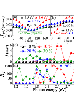
We next examined the effect of the mechanical strain on the behavior of the photocurrent, and found that the photocurrent still preserves the cosine dependence on the under the mechanical tension, since the mechanical tension applied uniformly along the direction does not change the symmetry. Examples are shown in Fig. 2(b) for the tension ratio of . However, it can be seen that the magnitude of the photocurrent is much larger than those without the mechanical tension. For comparisons, we obtained the maximum photocurrent at or for all of the photon energies under the different tension ratios, as shown in Fig. 2(c). It can be seen that the magnitude of the photocurrent is substantially enhanced by the mechanical tension for most of the photon energy from 1.2 eV to 3.2 eV. More specifically, Fig. 2(d) presents the increase ratio of the photocurrent under the mechanical tension with respect to that without the mechanical tension. Noticeably, at the , the are all greater than 1 for almost all of the photon energy except 3.1 eV (see the green squares), and the exceed for a number of photon energies. Moreover, the maximum ratio reaches to 1.5 for the at the photon energy of 1.8 eV. For the other , the is also greater than 1 for most of the photon energy.
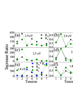
To understand this remarkable enhancement of the photocurrent under the mechanical tension, we first analyze the device asymmetry and examine its behavior for different tension ratio . The asymmetry is determined by the photon energy and also the tension ratio. We mainly focus on the photon energy of 2.9 eV, 2.5 eV and 1.8 eV, whose PGE photocurrent is enhanced most largely. The under different and its increase ratio are calculated for the = and with respect to that without the tension stress, respectively. Figs. 3(a,c,e) show the variation of the (the black stars) and (the green squares) with the for the photon energy of 2.9 eV, 2.5 eV and 1.8 eV, respectively, and Figs. 3(b,d,f) give the normalized ratios with respect to their largest value. From the normalized ratios, we observed that the overall trend of the matches monotonously with that of the for the different . This indicates that the enhancement of the PGE photocurrent is primarily determined by the change in the device asymmetry . Nevertheless, there are evident differences between the and at some , as shown in Figs. 3(a,c,e). It means that the enhancement of the photocurrent can not be exclusively attributed to the change in . The influences from the change in the optical absorption induced by the mechanical tension should also be considered. Therefore, we calculated the optical absorption coefficient of the monolayer phosphorene and the increase ratio under the different , as listed in Tab.I.
According to the Eqn. (4), in general the photocurrent should has a nonlinear dependence on the optical absorption. This nonlinear relationship is difficult to be expressed explicitly due to the tensor product of the and , which varies with the different photon energy and the mechanical strain. For example, for the photon energy of 2.5 eV (Fig. 3(c)), the change in the optical absorption seems to has a negligible influence on the photocurrent since the almost equals to the for most of the except that at the . In contrast, the is evidently less than the for the photon energy of 1.8 eV (Fig. 3(e)), which indicates a different dependence on the optical absorption. Interestingly, we found that at most of the the , as the blue triangles in Fig. 3(e) shows. This indicates that for the photon energy of 2.5 eV, the photocurrent has a linear dependence on both the optical absorption and the asymmetry in most of the cases.
| Tension | 0 | 5 | 10 | 12.5 | 15 | 17.5 | 20 | 30 | |
|---|---|---|---|---|---|---|---|---|---|
| 1.8 eV | 0.344 | 0.274 | 2.286 | 4.536 | 5.034 | 0.510 | 1.177 | 4.348 | |
| Rα | 0.798 | 6.648 | 13.191 | 14.639 | 1.483 | 3.424 | 12.644 | ||
| 2.5 eV | 1.521 | 1.892 | 3.651 | 5.073 | 5.558 | 4.046 | 6.410 | 6.246 | |
| Rα | 1.243 | 2.400 | 3.334 | 3.652 | 2.659 | 4.213 | 4.105 | ||
| 2.9 eV | 4.585 | 4.142 | 5.469 | 3.267 | 1.927 | 2.077 | 8.390 | 5.248 | |
| Rα | 0.903 | 1.193 | 0.713 | 0.420 | 0.453 | 1.830 | 1.145 | ||
| Bending | 0 | 0.9 | 1.3 | 2.5 | 3.9 | 5.3 | 6.3 | 8 | |
| 1.3 eV | 0.066 | 1.482 | 1.500 | 1.639 | 1.634 | 1.661 | 1.917 | 0.459 | |
| Rα | 22.390 | 22.663 | 24.773 | 24.699 | 25.109 | 28.976 | 6.943 | ||
| 1.8 eV | 0.180 | 1.965 | 1.980 | 1.999 | 2.010 | 2.044 | 2.017 | 2.165 | |
| Rα | 10.902 | 10.982 | 11.090 | 11.150 | 11.340 | 11.188 | 12.010 | ||
| 2.1 eV | 1.157 | 1.474 | 1.761 | 1.705 | 1.369 | 1.308 | 1.657 | 2.311 | |
| Rα | 1.273 | 1.522 | 1.473 | 1.183 | 1.130 | 1.432 | 1.996 |
We next consider the influence on the photocurrent by applying the mechanical bending on the free standing part of the phosphorene, as shown in Fig. 1(d). Obviously, the space inversion symmetry of the phosphorene is broken by the bending, while the whole device still remains the symmetry. Note that the mechanical tension does not change the symmetry of the phosphorenene. This means that the asymmetry of the device can be further increased by the mechanical bending, and therefore the PGE photocurrent would be enhanced further, as compared with that under the mechanical tension stress. We found that the photocurrent still holds the form of due to the unchanged symmetry of the device, as illustrated in Fig. 4(a). Evidently, the magnitude of the photocurrent is largely increased, as compared with those without the mechanical bending, as shown in Fig. 4(b). Moreover, the maximum photocurrent is 14.5 at 2.8 eV for , which is two times larger than that (6.6) under the tension stress (See Fig. 2(c)).
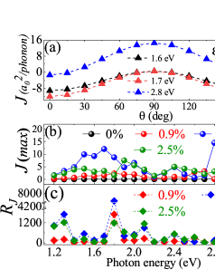
We observed that for a number of photon energies the is greater than 103, and the maximum reaches about 6.26 for the photon energy of 1.8 eV at the (the blue squares), which is about 4 times larger than that under the mechanical tension. At the photon energy of 1.3 eV, 1.8 eV and 2.1 eV, the photocurrent show the most large enhancement. We therefore give in Figs. 5(a,c,e) the and for these photon energies at different mechanical bending ratio of (1) 0.9%, (2) 1.3%, (3) 2.5%, (4) 3.9%, (5) 5.3%, (6) 6.3% and (7) 8%, and correspondingly give in Figs. 5(b,d,f) the normalized ratios. It can be seen that the trend of the is in a good agreement with that of the . This indicates that the remarkable enhancement of the photocurrent should also be mainly attributed to the increased device asymmetry . Nevertheless, the magnitude of the still differs from the . For the photon energy of 1.3 eV and 1.8 eV the is evidently less than the at the different , as shown in Figs. 5(a,c). Therefore, we should consider the influence of the change in the optical absorption. We found that the optical absorptions are all increased evidently at the different for the photon energy of 1.8 eV and 1.3 eV, as listed in Tab.I. This means that the photocurrent has a positive dependence on the optical absorption. In contrast, for the photon energy of 2.1 eV the has a much less deviation from the (Fig. 5(c)), which indicates that the change in the optical absorption has a very small influence on the photocurrent. Accordingly, we found that at every , which means that the optical absorption changes slightly under the mechanical bending for the photon energy of 2.1 eV. Besides, it is worth noting that under the mechanical bending the largest is 1254 at the =2.5% for the photon energy of 1.8 eV ( see Fig. 5(c)), while the largest is 415 achieved under the mechanical tension stress of for 2.9 eV (see Figs. 3(a)). This means that the device asymmetry is indeed further strengthened by the mechanical bending since it breaks the inversion symmetry of the phosphorene, while the mechanical tension stress does not.

We now obtained that the large enhancement of the PGE photocurrent under the appropriate mechanical strain is primarily due to the substantially increased device asymmetry, while the change in the optical absorption has a weaker contribution to the enhancement in most of the cases. This point is in agreement with the recent experimental findings, which showed that the change in the asymmetry of the LiNbO3 single-crystal by the mechanical compressive stress has a more important contribution on the enhancement of the PGE photocurrent than the change in the optical absorption.sci.adv.2019.5.eaau9199 Our results show that under an appropriate mechanical stress the PGE photocurrent can be substantially enhanced even by up to 3 orders of magnitude. In this regard, it is understandable that in the flexo-photovoltaic effect the mechanical gradient can induce a considerable enhancement of the PGE photocurrent for the SrTiO3 single crystals.Science.2018.360 Moreover, in our work the mechanical bending is even more effectively in improving the PGE photocurrent, which is in a good agreement with the essential point derived from the recent experiments that reducing the structure symmetry can largely enhance the PGE photocurrent in the WSe2 nanotubes.Nat.2019 Interestingly, recent experiments have also shown that the photocurrent generated in the flexible 2D PtSe2 phototransistorSmall.2018.14 and the 2D antimonene photodetectorNano.Horiz.2019 can be enhanced by the mechanical bending, which suggested that the mechanical tuned PGE may play a role. Therefore, our results on the enhancement of the PGE by the mechanical strain can provide insights on these related experiments, though further theoretical efforts are required to give the direct supports.
III.1 CONCLUSIONS
In summary, we have investigated the large enhancement of the PGE in the nickel-phosphorene-nickel photodetector tuned by the mechanical tension and bending, using the quantum transport calculations. The photocurrent can be substantially improved by 3 orders of magnitude by applying the appropriate mechanical tension and bending. The remarkable enhancement of the photocurrent is overall mainly due to the largely increased device asymmetry, although the change in the optical absorption can also play an important role in some cases. The mechanical bending can enhance the photocurrent more effectively than the tension stress, since it breaks the inversion symmetry of the phosphorene and hence strengthens largely the device asymmetry. Our results propose an approach to largely enhance the PGE photocurrent by applying the mechanical tension and bending, and shed lights on the applications of the PGE in the low-power 2D flexible optoelectronics and low-dimensional photodetections with high photoresponsivity, as well as give insights to the enhancement of the PGE achieved recently in experiments on the nanotubes and flexo-photovoltaic effects.
ACKNOWLEDGMENT
This work is supported by National Natural Science Foundation of China under Grant No.51871156 and 11704232, and also by National Key R&D Program of China under Grants No. 2017YFA0304203, 1331KSC, Shanxi Province 100-Plan Talent Program.
References
- (1) M. Long, P. Wang, H. Fang, and W. Hu, Progress, Challenges, and Opportunities for 2D Material Based Photodetectors, Adv. Funct. Mater. 29, 1803807 (2019).
- (2) N. Huo, and G. Konstantatos, Recent Progress and Future Prospects of 2D-Based Photodetectors, Adv. Mater., 30, 1801164 (2018).
- (3) H. Luo, B. Wang, E. Wang, X. Wang, Y. Sun, Q. Li, S. Fan, C. Cheng and K. Liu, Phase-transition modulated, high-performance dual-mode photodetectors based on WSe2/VO2 heterojunctions, Appl. Phys. Rev., 6, 041407 (2019).
- (4) A. Rogalski, M. Kopytko and P. Martyniuk, Two-dimensional infrared and terahertz detectors: Outlook and status, Appl. Phys. Rev., 6, 021316 (2019).
- (5) D. Wu, J. Guo, J. Du, C. Xia, L. Zeng, Y. Tian, Z. Shi, Y. Tian, X. J. Li, Y. H. Tsang and J. Jie, Highly polarization-sensitive, broadband, self-powered photodetector based on graphene/PdSe2/Germanium heterojunction, ACS nano, 13, 9907-9917 (2019).
- (6) Y. J. Zhang, T. Ideue, M. Onga, F. Qin, R. Suzuki, A. Zak, R. Tenne, J. H. Smet and Y. Iwasa, Enhanced intrinsic photovoltaic effect in tungsten disulfide nanotubes, Nature, 570, 349-353 (2019).
- (7) M.-M. Yang, D. J. Kim and M. Alexe, Flexo-photovoltaic effect, Science, 360, 904 (2018).
- (8) J. Kim, K. W. Kim, D. Shin, S. H. Lee, J. Sinova, N. Park and H. Jin, Prediction of ferroelectricity-driven Berry curvature enabling charge- and spin-controllable photocurrent in tin telluride monolayers, Nat. Commun., 10, 3965 (2019).
- (9) L. Xie and X. Cui, Manipulating spin-polarized photocurrents in 2D transition metal dichalcogenides, PNAS, 113, 3746 (2016).
- (10) S. Zamani, and R. Farghadan, Graphene Nanoribbon Spin-Photodetector, Phys. Rev. Applied, 10, 034059 (2018).
- (11) W. Shockley, The theory of pn junctions in semiconductors and pn junction transistors, ATT Tech. J., 28, 435 (1949).
- (12) H. Huang, J. Wang, W. Hu, L. Liao, P. Wang, X. Wang, F. Gong, Y. Chen, G. Wu, W. Luo, H. Shen, T. Lin, J. Sun, X. Meng, X. Chen and J. Chu, Highly sensitive visible to infrared MoTe2 photodetectors enhanced by the photogating effect, Nanotechnology, 27, 445201 (2016).
- (13) M. M. Furchi, D. K. Polyushkin, A. Pospischil and T. Mueller, Mechanisms of photoconductivity in atomically thin MoS2, Nano Lett., 14, 6165-6170 (2014).
- (14) H. Wang, C. Cheng, L. Zhang, H. T. Liu, Y. Zhao, Y. L. Guo, W. P. Hu, G. Yu and Y. Liu, Inkjet Printing Short-Channel Polymer Transistors with High-Performance and Ultrahigh Photoresponsivity, Adv. Mater, 26, 4683-4689 (2014).
- (15) C. Qian, J. Sun, L.-A. Kong, G. Gou, M. Zhu, Y. Yuan, H. Huang, Y. Gao and J. Yang, High-performance organic heterojunction phototransistors based on highly ordered copper phthalocyanine/para-sexiphenyl thin films, Adv. Funct. Mater., 27, 1604933 (2017).
- (16) M. Cao, C. Zhang, Z. Cai, C. Xiao, X. Chen, K. Yi, Y. Yang, Y. Lu and D. Wei, Enhanced photoelectrical response of thermodynamically epitaxial organic crystals at the two-dimensional limit, Nat. Commun., 10, 1-11 (2019).
- (17) V. I. Belinicher and B. I. Sturman, The photogalvanic effect in media lacking a center of symmetry, Sov. Phys. Usp., 23, 199 (1980).
- (18) S. D. Ganichev, H. Ketterl, W. Prettl, E. L. Ivchenko and L. E. Vorobjev, Circular photogalvanic effect induced by monopolar spin orientation in p-GaAs/AlGaAs multiple-quantum wells, Appl. Phys. Lett., 77, 3146-3148 (2000).
- (19) S. D. Ganichev and W. Prettl, Spin photocurrents in quantum wells, J. Phys. Condens. Matter, 15, R935 (2003).
- (20) M. M. R. Moayed, F. Li, P. Beck, J. C. Schober and K. K., Anisotropic circular photogalvanic effect in colloidal tin sulfide nanosheets, Nanoscale, 12, 6256 (2020).
- (21) Y. Xie, M. Chen, Z. Wu, Y. Hu, Y. Wang, J. Wang and H. Guo, Two-Dimensional Photogalvanic Spin-Battery, Phys. Rev. Appl., 10, 034005 (2018).
- (22) M. Chen, K. Lee, J. Li, L. Cheng, Q. Wang, K. Cai, E. E. M. Chia, H. Cheng, and H. Yang, Anisotropic Picosecond Spin-Photocurrent from Weyl Semimetal WTe2, Acs Nano, 14, 3539-3545 (2020).
- (23) R. von Baltz and W. Kraut, Theory of the bulk photovoltaic effect in pure crystals, Phys. Rev. B, 23, 5590 (1981).
- (24) A. M. Glass, D. V. D. Linde and T. J. Negran, High-voltage bulk photovoltaic effect and the photorefractive process in LiNbO3, Appl. Phys. Lett., 25, 233-235 (1974).
- (25) A. M. Burger, R. Agarwal, A. Aprelev, E. Schruba, A. Gutierrez-Perez, V. M. Fridkin and J. E. Spanier, Direct observation of shift and ballistic photovoltaic currents, Sci. Adv., 5, eaau5588 (2019).
- (26) Z. Ji, G. Liu, Z. Addison, W. Liu, P. Yu, H. Gao, Z. Liu, A. M. Rappe, C. L. Kane, E. J. Mele and R. Agarwal, Spatially dispersive circular photogalvanic effect in a Weyl semimetal, Nat. Mater., 18, 955 (2019).
- (27) G. Osterhoudt, L. K. Diebel, M. Gray, X. Yang, J. Stanco, X. Huang, B. Shen, N. Ni, P. J. W. Moll, Y. Ran and K. S. Burch, Colossal mid-infrared bulk photovoltaic effect in a type-I Weyl semimetal, Nature Materials, 18, 471 (2019).
- (28) J. Quereda, T. S. Ghiasi, J. You, J. V. Den Brink, B. J. Van Wees and C. H. V. Der Wal, Symmetry regimes for circular photocurrents in monolayer MoSe2, Nat. Commun., 9, 3346 (2018).
- (29) M. Nakamura, S. Horiuchi, F. Kagawa, N. Ogawa, T. Kurumaji, Y. Tokura and M. Kawasaki, Shift current photovoltaic effect in a ferroelectric charge-transfer complex, Nat. Commun., 8, 1 (2017).
- (30) J. E. Spanier, V. M. Fridkin, A. M. Rappe, A. R. Akbashev, A. Polemi, Y. Qi, Z. Gu, S. M. Young, C. J. Hawley, D. Imbrenda, G. Xiao, A. L. Bennett-Jackson and C. L. Johnson, Power conversion efficiency exceeding the Shockley-Queisser limit in a ferroelectric insulator, Nat. Photonics, 10, 611 (2016).
- (31) M. Dressel and T. Peterseim, Infrared investigations of the neutral-ionic phase transition in TTF-CA and its dynamics, Crystals, 7, 17 (2017).
- (32) J. Li and P. M. Haney, Circular photogalvanic effect in organometal halide perovskite CH3NH3PbI3, Appl. Phys. Lett., 109, 193903 (2016).
- (33) H. Zou, C. Zhang, H. Xue, Z. Wu and Z. L. Wang, Boosting the Solar Cell Efficiency by Flexo-photovoltaic Effect?, ACS nano, 13, 12259-12267 (2019).
- (34) S. Nadupalli, J. Kreisel and T. Granzow, Increasing bulk photovoltaic current by strain tuning, Sci. adv., 5, eaau9199 (2019).
- (35) Sturman, B.I. Fridkin,V.M.The Photovoltaic and Photorefractive Effects in Noncentrsymmetric Materials (Gordon and Breach Science Publishers.1992).
- (36) P. Zhao, H. Yang, J. Li, H. Jin, W. Wei, L. Yu, B. Huang and Y. Dai, Design of new photovoltaic systems based on two-dimensional group-IV monochalcogenides for high performance solar cells, J. Mater. Chem. A, 5, 2414 (2017).
- (37) Q. Wang, J. Li, Y. Liang, B. Wang and Y. Nie, BX1-BX2 (X1, X2 = P, As, Sb) lateral heterostructure: novel and efficient two-dimensional photovoltaic materials with ultra-high carrier mobilities, J. Mater. Chem. A, 7, 10684 (2019).
- (38) V. I. Belinicher, E. L. Ivchenko and B. I. Sturman, Kinetic theory of the displacement photovoltaic effect in piezoelectrics, Sov. Phys. JETP, 56, 359 (1982).
- (39) T. Rangel, B. M. Fregoso, B. S. Mendoza, T. Morimoto, J. E. Moore and J. B. Neaton, Large bulk photovoltaic effect and spontaneous polarization of single-layer monochalcogenides, Phys. Rev. Lett., 119, 067402 (2017).
- (40) S. M. Young and A. M. Rappe, First Principles Calculation of the Shift Current Photovoltaic Effect in Ferroelectrics, Phys. Rev. Lett., 109, 116601 (2012).
- (41) S. M. Young, F. Zheng and A. M. Rappe, First-Principles Calculation of the Bulk Photovoltaic Effect in Bismuth Ferrite, Phys. Rev. Lett., 109, 236601 (2012).
- (42) T. Morimoto and N. Naoto Nagaosa, Topological nature of nonlinear optical effects in solids, Sci. Adv., 2, e1501524 (2016).
- (43) K. N. Okada, N. Ogawa, R. Yoshimi, A. Tsukazaki, K. S. Takahashi, M. Kawasaki and Y. Tokura, Enhanced photogalvanic current in topological insulators via Fermi energy tuning, Phys. Rev. B, 93, 081403(R) (2016).
- (44) E. J. Konig, H.-Y. Xie, D. A. Pesin and A. Levchenko, Photogalvanic effect in Weyl semimetals, Phys. Rev. B, 96, 075123 (2017).
- (45) V. M. Kovalev and I. G. Savenko, Photogalvanic currents in dynamically gapped transition metal dichalcogenide monolayers, Phys. Rev. B, 99, 075405 (2019).
- (46) B. M. Fregoso, Bulk photovoltaic effects in the presence of a static electric field, Phys. Rev. B, 100, 064301 (2019).
- (47) H. Soifer, A. Gauthier, A. F. Kemper, C. R. Rotundu, S.-L. Yang, H. Xiong, D. Lu, M. Hashimoto, P. S. Kirchmann, J. A. Sobota, and Z.-X. Shen, Band resolved imaging of photocurrent in a topological insulator, Phys. Rev. Lett., 122, 167401 (2019).
- (48) A. Avdoshkin, V. Kozii and J. E. Moore, Interactions Remove the Quantization of the Chiral Photocurrent at Weyl Points, Phys. Rev. Lett., 124, 196603 (2020).
- (49) Y. Gao, Y. Zhang and D. Xiao, Tunable Layer Circular Photogalvanic Effect in Twisted Bilayers, Phys. Rev. Lett., 124, 077401 (2020).
- (50) S. V. Zhukovsky, V. E. Babicheva, A. B. Evlyukhin, I. E. Protsenko, A. V. Lavrinenko and A. V. Uskov, Giant Photogalvanic Effect in Noncentrosymmetric Plasmonic Nanoparticles, Phys. Rev. X, 4, 031038 (2014).
- (51) G. Kresse and J. Hafner, Ab Initio Molecular Dynamics for Liquid Metals, Phys. Rev. B: Condens. Matter, 47, 558-561 (1993).
- (52) W. Kohn and L. J. Sham, Self-consistent equations including exchange and correlation effects, Phys. Rev. B, 140, 1133-1148 (1965).
- (53) Y. Q. Xie, M. Y. Chen, Z. Wu, Y. Hu, Y. Wang, J. Wang and H. Guo, Two-dimensional photogalvanic spin-battery, Two-dimensional photogalvanic spin-battery, Phys. Rev. Appl., 10, 034005 (2018).
- (54) Q. Wei and X. Peng, Superior mechanical flexibility of phosphorene and few-layer black phosphorus, Appl. Phys. Lett., 104, 251915 (2014).
- (55) W. Zhu, M. N. Yogeesh, S. Yang, S. H. Aldave, J.-S. Kim, S. Sonde and D. Akinwande, Flexible Black Phosphorus Ambipolar Transistors, Circuits and AM Demodulator, Nano Lett., 15, 1883 (2015).
- (56) G. Wang, G. C. Loh, R. Pandey and S. P. Karna, Out-of-plane structural flexibility of phosphorene, Nanotechnology, 27, 055701 (2016).
- (57) J. P. Perdew, K. Burke and M. Ernzerhof, Generalized gradient approximation made simple, Phys. Rev. Lett., 77, 3865 (1996).
- (58) H. J. Monkhorst and J. D. Pack, Special points for Brillouin-zone integrations, Phys. Rev. B, 13, 5188 (1976).
- (59) L. E. Henrickson, Nonequilibrium photocurrent modeling in resonant tunneling photodetectors, J. Appl. Phys., 91, 6273-6281 (2002).
- (60) J. Z. Chen, Y. B. Hu and H. Guo, First-principles analysis of photocurrent in graphene PN junctions, Phys. Rev. B, 85, 155441 (2012).
- (61) Y. Q. Xie, L. Zhang, Y. Zhu, L. Liu and H. Guo, Photogalvanic effect in monolayer black phosphorus, Nanotechnology, 26, 455202 (2015).
- (62) L. Zhang, K. Gong, J. Z. Chen, L. Liu, Y. Zhu, D. Xiao and H. Guo, Generation and transport of valley-polarized current in transition-metal dichalcogenides, Phys. Rev. B, 90, 195428 (2014).
- (63) J. Chen, L. W. Zhang, L. Zhang, X. L. Zheng, L. Xiao, S. Jia and J. Wang, Photogalvanic effect induced fully spin polarized current and pure spin current in zigzag SiC nanoribbons, Phys. Chem. Chem. Phys., 20, 26744 (2018).
- (64) S. Datta, Linear-response formulation for mesoscopic systems with arbitrary interactions, Phys. Rev. B, 46, 9493 (1992).
- (65) O. Madelung and H. J. Juretschke, Introduction to Solid State Theory, Springer Series in Solid State Sciences, 2, (1978).
- (66) Y. Luo, Y. Hub and Y. Xie, Highly polarization-sensitive, visible-blind and selfpowered ultraviolet photodetection based on two-dimensional wide bandgap semiconductors: a theoretical prediction, J. Mater. Chem. A., 7, 27503 (2019).
- (67) T.-Y. Su, H. Medina, Y.-Z. Chen, S.-W. Wang, S.-S. Lee, Y.-C. Shih, C.-W. Chen, H. C. Kuo, F.-C. Chuang and Y.-L. Chueh, Phase-engineered PtSe2-layered films by a plasma-assisted selenization process toward all PtSe2-based field effect transistor to highly sensitive, flexible, and wide-spectrum photoresponse photodetectors, Small, 14, 1800032 (2018).
- (68) Q. Xiao, C.-X. Hu, H.-R. Wu, Y.-Y. Ren, X.-Y. Li, Q.-Q. Yang, G.-H. Dun, Z.-P. Huang, Y. Peng, F. Yan, Q. Wang and H.-L. Zhang, Antimonene-based flexible photodetector, Nano. Horiz., 5, 124-130 (2020).