GW band structure of monolayer MoS2 using the SternheimerGW method and effect of dielectric environment
Abstract
Monolayers of transition-metal dichalcogenides (TMDs) hold great promise as future nanoelectronic and optoelectronic devices. An essential feature for achieving high device performance is the use of suitable supporting substrates, which can affect the electronic and optical properties of these two-dimensional (2D) materials. Here, we perform many-body GW calculations using the SternheimerGW method to investigate the quasiparticle band structure of monolayer MoS2 subject to an effective dielectric screening model, which is meant to approximately describe substrate polarization in real device applications. We show that, within this model, the dielectric screening has a sizable effect on the quasiparticle band gap, for example the gap renormalization is as large as 250 meV for MoS2 with model screening corresponding to SiO2. Within the G0W0 approximation, we also find that the inclusion of the effective screening induces a direct band gap, in contrast to the unscreened monolayer. We also find that the dielectric screening induces an enhancement of the carrier effective masses by as much as 27% for holes, shifts plasmon satellites, and redistributes quasiparticle weight. Our results highlight the importance of the dielectric environment in the design of 2D TMD-based devices.
I Introduction
Semiconducting compounds of layered transition-metal dichalcogenides (TMDs) in their two-dimensional (2D) forms have exceptional properties. They undergo an indirect-to-direct band gap transition in the monolayer limit,Mak et al. (2010); Kuc et al. (2011) and they exhibit a strong spin-orbit coupling,Zibouche et al. (2014a) and tightly bound excitonsHe et al. (2014); Steinhoff et al. (2018); Waldecker et al. (2019); Deilmann and Thygesen (2019); Gjerding et al. (2020) and trions,Mak et al. (2013); Florian et al. (2018); Goswami et al. (2019) which give rise to interesting spin-valley physics.Cao et al. (2012); Refaely-Abramson et al. (2018); Yong et al. (2019); Zhang et al. (2019) They also offer the possibility of designing a variety of van der Waals heterostructures.Yu et al. (2013a); Utama et al. (2019) In the past decade there have been significant advances in the synthesis and fabricationChhowalla et al. (2013) of TMDs, opening up many opportunities in applications for nanoelectronics and optoelectronics, including photodetectors,Lopez-Sanchez et al. (2013) lasers,Salehzadeh et al. (2015) light emitting diodes,Withers et al. (2015) memory devices,Roy et al. (2013) sensors,Zhang et al. (2015) and field-effect transistors.Radisavljevic et al. (2011); Yu et al. (2013b) Two-dimensional TMDs exhibit strong Coulomb interactions associated with the weak dielectric screening in two dimensions.Cudazzo et al. (2011); Berkelbach et al. (2013) Consequently, the polarization of the supporting substrate modifies electron-electron and electron-hole interactions, thus renormalizing the quasiparticle gap and reducing the exciton binding energies. For example, the measured electronic band gap on a SiO2 substrate is 2.10 eV,Zhou et al. (2016); Kerelsky et al. (2017); Goryca et al. (2019); Klein et al. (2019) whereas values of 1.9 eVPark et al. (2018) and 2.40 eVHuang et al. (2015) have been reported on gold and graphite substrates, respectively. The exciton binding energy spans a wide range, between 0.2 eV and 0.9 eV,Cheiwchanchamnangij and Lambrecht (2012); Klein et al. (2019); Cao (2015); Park et al. (2018); Qiu et al. (2013); Klots et al. (2014); Goryca et al. (2019) depending on the substrate. Several experimental and theoretical studies reported substrate-dependent electronic and optical properties of these atomically thin TMDs, such as variations in the carrier mobilities and transport properties,Radisavljevic and Kis (2013); Bao et al. (2013); Liu et al. (2013); Yu et al. (2016a); Huo et al. (2018) exciton binding energies and lifetimes,Korn et al. (2011); Cheiwchanchamnangij and Lambrecht (2012); Shi et al. (2013a); Lin et al. (2014); Cao (2015); Palummo et al. (2015) luminescence efficiency,Sercombe et al. (2013); Buscema et al. (2014); Scheuschner et al. (2014); Yu et al. (2016b) and band gap renormalization.Zhang et al. (2014); Bruix et al. (2016); Rigosi et al. (2016); Zhou et al. (2016); Kerelsky et al. (2017); Klein et al. (2019) This sensitivity to the substrate calls for an investigation of the role of environmental screening in the electronic properties of 2D materials.
Previous studies in this field focused on the effect of the substrate on the band gap and the binding energies.Hüser et al. (2013); Lin et al. (2014); Ryou et al. (2016); Park et al. (2018); Steinhoff et al. (2018); Waldecker et al. (2019) Since calculations with explicit substrates to capture the screening of a semi-infinite bulk insulator are currently beyond reach, all previous work relied on simple models of substrate screening. Here we also model the substrate screening using an effective dielectric continuum, and we expand on previous work by investigating the effect of dielectric screening on the quasiparticle bands, carrier effective masses, spectral density and plasmon satellites. To this aim, we perform state-of-the-art many-body GW calculations for the archetypal TMD monolayer MoS2. Substrate polarization is accounted for within a simple model whereby we screen the Coulomb potential entering the calculation of the polarizability within the random phase approximation. To make the analysis directly relevant to experiments, we choose the dielectric constants corresponding to hexagonal boron nitride (h-BN) and SiO2, which are commonly used with TMDs. We show that the renormalization of quasiparticle energies can be significant; for example the band gap of monolayer MoS2 decreases by as much as 250 meV when considering a SiO2 substrate, and the hole effective mass increases by 27%. Furthermore, we find that the model dielectric environment changes the nature of the gap from indirect to direct, and shifts plasmon satellites.
This paper is organized as follows. In Sec. II we briefly review the SternheimerGW method used in this work, we discuss computational details, and we provide numerical convergence tests. In Sec. III we report our results on the quasiparticle band structure of monolayer MoS2 in the presence of an effective dielectric screening, we analyze the renormalization of the band gap and effective masses, and we discuss the influence of the dielectric environment on the spectral function and plasmon satellites. In Sec. IV we summarize our findings and offer our conclusions.
II Methods
II.1 The SternheimerGW method
The GW methodHedin (1965); Hybertsen and Louie (1986); Onida et al. (2002); Golze et al. (2019) has emerged as the most successful ab initio approach for calculating many-body quasiparticle band structures in semiconductors. The method is based on the calculation of the electron self-energy, which includes exchange and correlation effects via the dynamically screened Coulomb interaction. The screened Coulomb interaction is most often calculated within the random-phase approximation (RPA), starting from Kohn-Sham wavefunctions obtained within density functional theory (DFT) Kohn and Sham (1965).
Standard implementations of the GW methods obtain the electron Green’s function and the RPA polarizability by using an expansion over unoccupied Kohn-Sham states.Kresse and Furthmüller (1996); Deslippe et al. (2012); Gonze et al. (2020) Although very successful, in this approach the convergence with respect to unoccupied states is challenging, which results in a heavy computational load. To circumvent this bottleneck, several groups have been pursuing direct calculations of and/or using the Sternheimer equation or variants of this method.Baroni et al. (1987, 2001); Umari et al. (2009, 2010); Govoni and Galli (2015) In this work we employ the SternheimerGW method that we developed, Schlipf et al. (2020) in which both the screened Coulomb interaction and the electron Green’s function are evaluated using solely the occupied Kohn-Sham states. Below we briefly review this methodology. More details and the derivation of key equations can be found in Refs. Schlipf et al., 2020; Lambert and Giustino, 2013; Giustino et al., 2010.
The Green’s function and the screened Coulomb interaction are expressed in terms of the space coordinate , while and are treated as parametric space and frequency variables. The Green’s function is calculated by solving the inhomogeneous linear system of equations for all occupied states
| (1) |
Here, corresponds to the single-particle Kohn-Sham Hamiltonian and is the Dirac delta function.
The screened Coulomb interaction within the RPABohm and Pines (1951); Pines and Bohm (1952); Bohm and Pines (1953) can be obtained with the procedure outlined below. When the system is subject to a perturbation , the corresponding change in the charge density is given by
| (2) |
where are the frequency-dependent variations of the occupied single-particle wavefunctions. These variations are obtained by solving the following Sternheimer equation
| (3) |
The operator projects onto the occupied manifold, and are the corresponding Kohn-Sham energy eigenvalues. There are two methods for choosing the perturbation that yield . In the direct (non-self-consistent) approach, the perturbation is set to the bare Coulomb potential . From the variation in the charge density, the RPA dielectric function is evaluated as
| (4) |
The screened Coulomb interaction is then calculated by inverting via
| (5) |
In the self-consistent method, the perturbation is set to the screened Coulomb interaction ). This scheme initializes the perturbation to the bare Coulomb interaction . Then, the induced variation in the charge density generates a Hartree potential that screens the bare Coulomb interaction through
| (6) |
The updated screened Coulomb interaction , given by
| (7) |
is subsequently used to evaluate the next density response. This process is iterated until convergence is reached.
The self-energy, , is obtained as the product of the Green’s function and the screened Coulomb interaction
| (8) |
and the quasiparticle energies can thus be determined as
| (9) |
where , , and are, respectively, the Kohn-Sham DFT eigenvalues, wavefunctions, and the expectation value of the exchange-correlation potential of the band. is the quasiparticle renormalization factor that defines the quasiparticle weight carried by the excitation. The SternheimerGW method provides the possibility of calculating the complete energy- and momentum-resolved spectral function , a physical observable that can be extracted from angle-resolved photoemission spectroscopy (ARPES) measurements. is calculated as
| (10) |
in which and indicate the real and imaginary parts of the G0W0 self-energy, and .
II.2 Computational details
Ground-state calculations are carried out using density functional theory as implemented in the Quantum ESPRESSO package.Giannozzi et al. (2017, 2009) The Kohn-Sham wavefunctions and energies are calculated using the Perdew-Burke-Ernzerhof (PBE) functional.Perdew et al. (1996) A plane-wave basis is used with energy and charge-density cutoffs of 50 Ry and 200 Ry, respectively. We approximate the core-valence interactions via norm-conserving pseudopotentials, explicitly including the 4 and 4 semicore electrons of Mo. The Brillouin zone (BZ) integration is sampled using a Monkhorst-Pack -point grid.Monkhorst and Pack (1976) The atomic positions are relaxed at the experimental lattice constant = 3.16 Å. To avoid spurious interactions between periodically repeated slabs, the size of the computational cell, including monolayer and vacuum, is set to 20 Å in the out-of-plane direction, unless otherwise stated.
We perform G0W0 calculations starting from the PBE wavefunctions and energy eigenvalues. The dielectric matrix is computed within the random phase approximation using either the Godby-Needs plasmon-pole approximation (PPA)Godby and Needs (1989) with an imaginary pole energy of 16 eV, or using full frequency integration (FF), as implemented in the SternheimerGW code.Schlipf et al. (2020); Lambert and Giustino (2013); Giustino et al. (2010) The FF integration is performed along the imaginary axis using 65 discrete frequencies in the interval of 0 eV to 240 eV. We obtain the FF self-energy on the real axis using an analytic continuation following the adaptive Antoulas-Anderson method.Nakatsukasa et al. (2018)
To avoid spurious Coulomb interactions between electrons belonging to periodic images of the monolayer, we truncate the Coulomb interaction , in the calculation of both the dielectric function, , and the screened Coulomb interaction, . In particular, we employ a 2D truncation scheme in reciprocal space, using the expression from Refs. Rozzi et al., 2006 and Ismail-Beigi, 2006: . Here is the cutoff distance in the out-of-plane direction. At the DFT level, we truncate the bare Coulomb potential using the scheme of Ref. Sohier et al., 2017, which speeds up the convergence of the GW calculations with respect to the Brillouin zone grid. We note that this truncation is important: without truncation the GW band gap would be underestimated by about 0.26 eV.
In order to take into account the effect of substrate polarization, we renormalize the screened Coulomb interaction by the effective background dielectric constant () through
| (11) |
where refers to the relative dielectric constant of the substrate.Hwang et al. (2007); Polini et al. (2008); Hwang and Das Sarma (2008)
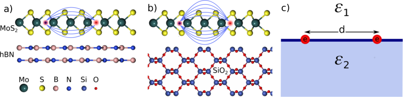
This effective dielectric constant is obtained by evaluating the Coulomb interaction between two point charges at the (mathematically sharp) interface between vacuum and a semi-infinite dielectric continuum, as shown in Fig. 1. Jackson (1999) Using this approach we model two substrate materials, SiO2 ()Robertson (2004) and a monolayer or a few layers of h-BN ().Hyder (1976); Kim et al. (2012) Figure. 1 shows a qualitative schematic of the systems that we model, however we emphasize that our calculations contain a single layer of MoS2, without substrate atoms.
II.3 Numerical convergence tests
| mesh | Irreducible points | VBM | CBM | QP gap |
|---|---|---|---|---|
| 12 | ||||
| 19 | ||||
| 27 | ||||
| 37 | ||||
| 48 |
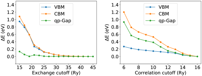
For accurate results GW calculations require the convergence of several numerical parameters. In this section, we discuss the dependence of the band gap and the energy of the band extrema with respect to the energy cutoff for exchange and correlation, as well as the sampling of the Brillouin zone using the PPA.
First, we focus on the convergence of the quasiparticle band gap (QP gap) and the valence band maximum (VBM) and conduction band minimum (CBM) at the point, with respect to the exchange () and the correlation () energy cutoffs. The relative changes compared to the converged values are shown in Fig. 2. To study the convergence of we set a correlation cutoff (1 Ry = 13.605 eV); conversely, to study the convergence with respect to , the exchange cutoff is set to . In both convergence tests, the BZ is sampled using a -point mesh (27 irreducible points) for the dielectric matrix and the screened Coulomb interaction. Figure. 2a shows that VBM and CBM are well converged for above 35 Ry, increasing by only 12 meV when we increase the cutoff all the way to 45 Ry. Since both band extrema converge from the top at a similar rate, the QP gap converges much faster, and is accurate to within 2 meV already for . Figure. 2b shows that the convergence with respect to is somewhat slower, but the changes in the VBM, CBM, and QP gap from Ry to 16 Ry are of 15 meV, 31 meV, and 16 meV respectively. For , the QP gap is found to be 2.70 eV, which is remarkably (and probably coincidentally) the same value as reported in experiments on suspended layers.Lin et al. (2014)
Next, we focus on the number of grid points used for sampling the BZ to evaluate the dielectric matrix and the screened Coulomb interaction within the PPA. Table 1 reports the convergence of the QP gap, the VBM, the CBM at the high-symmetry K point at fixed energy cutoffs and . A -point grid of is necessary to converge the self-energy with 50 meV accuracy. The resulting QP gap at the K point is in very good agreement with previous GW calculations, yielding 2.60–2.80 eV.Cheiwchanchamnangij and Lambrecht (2012); Shi et al. (2013b); Hüser et al. (2013); Jin et al. (2015a) As in the present work, these previous calculations employ the experimental lattice parameter. Differences between reported band gaps arise from differences in the GW calculations, specifically the Coulomb truncation and the vacuum size. Despite such differences, our calculations also indicate that the G0W0 band gap of a pristine MoS2 monolayer is indirect. We do not include spin-orbit coupling in our calculations, because the resulting energy splittings at the K point amount to 3 meV (CBM) and 147 meV (VBM) at the DFT level, which is below the numerical precision of our GW calculations.
III Results and Discussion
III.1 Quasiparticle band gap and band structures
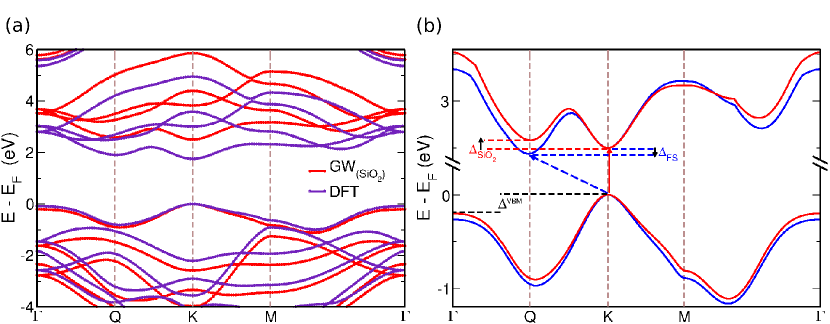
In this section we discuss our results for the quasiparticle band gap and band structure of monolayer MoS2, as obtained by considering a layer in vacuum, the effective screening from a SiO2 substrate, and the effective screening resulting from h-BN. The following results correspond to exchange and correlation cutoffs and , and a -point grid. In Fig. 3a, we compare the DFT and the G0W0/PPA band structure of a MoS2 monolayer in the presence of the model dielectric screening corresponding to SiO2. The G0W0 correction is not uniform throughout the Brillouin zone, so that not only the band gap but also the effective masses are modified (see Sec. III.2). In Table 2, we compare the calculated QP gap, VBM, and CBM at the high-symmetry K point of the unscreened [“freestanding” (FS)] MoS2 monolayer, with a monolayer in the presence of screening from an effective substrate with the dielectric constants of h-BN or SiO2. When using full frequency integration, the band extrema shift to lower energies, and the QP gap is reduced compared to that in the PPA model. This reduction ranges from 40 meV for the unscreened monolayer to 80 meV for the screened monolayer.
We find that the model substrate screening renormalizes the absolute quasiparticle energies of the VBM and CBM. As a consequence, the quasiparticle band gap is also reduced as compared to the unscreened monolayer. In particular, we find a reduction of the band gap by 180(140) meV when using FF(PPA) frequency integration for h-BN, and of 250(210) meV for SiO2. This reduction is consistent with the notion that the Coulomb energy required for adding/removing an electron in monolayer MoS2 should be reduced by the dielectric screening of the substrate.
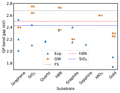
In line with our finding, previous experimental and theoretical work indicates the sensitivity of the QP gap to the dielectric screening environment, as shown in Fig. 4. In the case of the SiO2 substrate, scanning tunneling spectroscopy (STS) measurements obtain a QP gap of 2.1 eV.Zhou et al. (2016); Kerelsky et al. (2017); Klein et al. (2019) However, optical absorption measurements on the same sample used for STS in Ref. Klein et al., 2019 yield a gap of 2.44 eV. This latter value agrees with our FF QP gap (2.43 eV) for monolayer MoS2 with model screening corresponding to SiO2. Ref. Klein et al., 2019 argues that the tunneling gap is underestimated due to band-tail states near the conduction band minimum. Overall, the calculated band gaps from the literature, which we reproduce in Fig. 4, are in qualitative agreement with experiments. However, the magnitude of the QP gap renormalization is generally underestimated. Particularly good agreement between theory and experiments is found for the MoS2 monolayer on a h-BN substrate. The carefully converged GW QP gap (2.36 eV) from Ref. Utama et al., 2019 is very similar to the QP gap measured by STS (2.35 eV) in Ref. Klein et al., 2019. In our calculations, when we consider FF integration and corresponding to the dielectric constant of bulk h-BN, We obtain a QP gap of 2.35 eV, which is in excellent agreement with the above theoretical and experimental values.
| at K point | VBM | CBM | QP gap | |||
|---|---|---|---|---|---|---|
| Substrate | PPA | FF | PPA | FF | PPA | FF |
| FS | ||||||
| h-BN | ||||||
| SiO2 | ||||||
One interesting result of our calculations is that the screening of the substrate changes the character of the QP gap. As mentioned above, G0W0 predicts an indirect QP gap for the free-standing MoS2 monolayer at the experimental lattice parameter (3.16 Å). When we employ a model dielectric screening with the dielectric constants of SiO2 or h-BN, we find a direct QP gap. Figure. 3b illustrates this change in between the free-standing monolayer and a monolayer in the presence of model dielectric screening corresponding to an SiO2 substrate. In the presence of substrate screening, the CBM at the midpoint, Q, of the high-symmetry –K path (see Fig. 3) raises above the CBM at the K point as compared to the unscreened case. Introducing the energy difference = CBMK - CBMQ, we find , , and using the FF method. In the PPA calculations these differences are less pronounced: , , and . This result indicates that the screening-induced renormalization is more significant at the K point, and especially so when using FF integration. Unlike the CBM, the maximum of the valence band remains at the K point irrespective of substrate screening. The energy difference between the VBMs at the K and point are 0.23 eV, 0.19 eV and 0.17 eV for the unscreened, the h-BN-screened, and the SiO2-screened monolayer, respectively. Again the PPA yields smaller differences, in the range of 20–30 meV. It should be noted that to predict a direct band gap at the G0W0 level, a full geometry relaxation (lattice parameters and atomic positions) is needed. Furthermore, self-consistent GW calculations also lead to direct band gap in the MoS2 monolayerCheiwchanchamnangij and Lambrecht (2012); Shi et al. (2013b) as observed in photoluminescence measurements.Mak et al. (2010); Lin et al. (2014)
Overall, the present results show that the dielectric environment alters qualitatively and quantitatively the QP gap of monolayer MoS2. It is natural to expect the same behavior for other monolayer TMDs. In addition to the effect of dielectric screening from a uniform semi-infinite substrate, which we consider here, it is expected that several other effects will contribute to renormalizing QP levels in these systems, for example the atomic-scale structure of the TMD/substrate interface, and the possible presence of interface dipoles, strain, moirés, and charge transfer. These effects should be considered by performing calculations using explicit substrates. The advantage of the simple model adopted here is that it includes long-range electrostatic effects that would not be captured by calculations using a substrate slab of finite thickness.
III.2 Electron and hole effective masses
The effective masses of electrons and holes at the K point are calculated along the high-symmetry K– and K–M lines. We evaluate the second derivatives of the band curvatures numerically, using a step Å-1 around the K point. Since in the SternheimerGW method the Green’s function and the screened Coulomb interaction are computed separately, we can directly determine quasiparticle energies for arbitrary -points, without using interpolation techniques. Our calculated effective masses are shown in Table 3. The electron and hole effective masses obtained within DFT are 0.43 and 0.52 , respectively, consistent with previously reported values Zibouche et al. (2014b, a) ( indicates the free electron mass). In the DFT calculations we do not include the substrate screening effect, so the reported DFT mass is independent of substrate screening. The G0W0 effective masses for the unscreened MoS2 monolayer are in a good agreement with previous GW data available in the literature, in the range of 0.35–0.40 Cheiwchanchamnangij and Lambrecht (2012); Shi et al. (2013b); Molina-Sánchez et al. (2015); Qiu et al. (2013) for electrons and 0.39–0.49 Cheiwchanchamnangij and Lambrecht (2012); Shi et al. (2013b); Molina-Sánchez et al. (2015) for holes. In the presence of model substrate screening, the effective masses are heavier than for the unscreened monolayer (see Table 3). This is consistent with Fig. 3b, where we see that band curvatures at the K point are more pronounced when considering screening from SiO2. We find that, for the model with the screening corresponding to a h-BN (SiO2) substrate, the electron effective mass is enhanced by 5% (8%) whereas the hole effective mass increases by 17% (27%) with respect to the unscreened layer. As for the quasiparticle shifts, the effective mass enhancement due to the screening is more pronounced for calculations performed with FF integration rather than the PPA.
| at K point | ||||||
|---|---|---|---|---|---|---|
| Substrate | PPA | FF | DFT | PPA | FF | DFT |
| FS | ||||||
| h-BN | ||||||
| SiO2 | ||||||
Effective masses have been measured for a MoS2 monolayer separated from a MoS2 bulk compound by intercalating potassium using angle-resolved photoemission spectroscopy (ARPES).Eknapakul et al. (2014) The extracted effective masses at the K point are and . These values are significantly higher than in our calculations and previous theoretical work. The difference could originate from the heavy doping of the conduction band with electrons by the potassium intercalation, which would induce metallic screening.Eknapakul et al. (2014); Miwa et al. (2015) This interpretation is consistent with the fact that the gap extracted from ARPES is , eV, is significantly smaller than other measured optical gaps and calculated quasiparticle gaps (see Fig. 4). We also note that our calculations do not take into account the intercalant and electron-phonon interactions, which can both contribute to modifying the effective masses.
Additional ARPES measurements of the hole effective mass on different substrates have been reported. Ref. Jin et al., 2015b measured the hole effective mass for a suspended monolayer () and for a monolayer on SiO2 (). Their findings are very close to our calculations. Ref. Miwa et al., 2015; Dendzik et al., 2015 reported a hole effective mass of for a MoS2 monolayer grown on a gold substrate. Larger values of the effective masses, Kim et al. (2016) and Frégnaux et al. (2016), have been reported for MoS2 grown on SiO2 by chemical vapor deposition. Also in this case, the high doping level is expected to contribute an effective mass enhancement compared to exfoliated monolayers.Frégnaux et al. (2016)
Our calculated reduced electron-hole effective masses, , for the unscreened monolayer and for h-BN and SiO2 screening, are 0.20 , 0.22 , and 0.23 , respectively. These values should be compared with the measured exciton’s reduced mass , as obtained from magneto-optical spectroscopy experiments.Goryca et al. (2019) The slight difference may be due to the fact that, in the experiment, the MoS2 monolayer is encapsulated between slabs of h-BN, therefore the screening is enhanced compared to our calculations.
III.3 Self-energy and spectral function
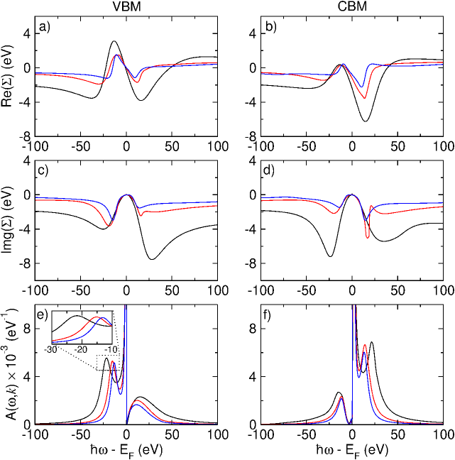
In this section, we discuss the effect of the dielectric screening on the electron self-energy, the spectral function, and the related incoherent plasmonic structure. For these calculations it is necessary to employ FF integration as opposed to the PPA. Figures. 5a-d show the frequency-dependent real and imaginary parts of the self-energy of the VBM and the CBM at the K point, for both the unscreened and screened MoS2 monolayer. The real part determines the quasiparticle shift and renormalization, the imaginary part determines the quasiparticle broadening and lifetimes. We can see that both Re() and Im() have a pronounced structure in the range of 15–25 eV, which arises from plasmon excitations. In fact, the electron energy loss spectra of MoS2 monolayer exhibit the characteristic of low-energy and high-energy plasmon resonances called and at 7.6 eV and 15.6 eV, respectively, which arise from the collective excitation of the Mo and S states.Liang and Cundy (1969); Johari and Shenoy (2011) Here, the spectral function A() in Figs. 5e,f clearly shows a plasmon satellite at around 22 eV, arising from the excitation of the high-energy plasmons.Liang and Cundy (1969); Johari and Shenoy (2011) On the other hand, the low-energy plasmons are not visible; these features possibly overlap with the broad main quasiparticle peaks. We emphasize that the energy and intensity of these plasmonic satellites are not captured correctly by G0W0, which is known to overestimate the binding energy of satellites. For an accurate description of these features one would need to perform cumulant expansion calculations.Guzzo et al. (2012); Lischner et al. (2013); Guzzo et al. (2014); Kas et al. (2014); Caruso et al. (2015); Caruso and Giustino (2016) Earlier studies of plasmon satellites of TMDs within the cumulant expansion method can be found in Ref. Caruso et al., 2015.
When introducing substrate screening within the simplified model adopted in this work, these structures become less intense, and shift to lower binding energies. This shift can be rationalized in terms of the Drude model, whereby the plasma frequency is given by , where , and are the electron density, charge and mass, respectively.Kittel (2004) When substituting the permittivity of vacuum with the effective dielectric constant of the substrate , the plasma frequency is reduced with respect to the unscreened monolayer, . The inset in Fig. 5e shows that our calculated shift in the plasma peaks is consistent with Drude’s model. In fact, we find that the unscreened plasmon peak at 22 eV shifts to around 16 eV and 13 eV when we consider screening corresponding to h-BN and SiO2 substrates, respectively.
From the real part of the self-energy we can evaluate the quasiparticle renormalization factors, . For the VBM/CBM states at we find /0.77, 0.79/0.83, and 0.80/0.87 for the unscreened, and h-BN- and SiO2-screened monolayers, respectively. These values indicate a weakly correlated electron system. The larger values associated with the larger screening are consistent with a lower transfer of quasiparticle weight to the plasmon satellites, and hence reduced correlations, as can be seen in the spectral function plots in Figs. 5e,f .
IV Conclusions
In summary, we investigated the dielectric screening effect of a substrate on the quasiparticle properties of monolayer MoS2 using the first-principles SternheimerGW method and a simplified effective dielectric model to account for substrate polarization. We showed that the additional screening by the substrate reduces the quasiparticle band gap by as much as 250 meV.
G0W0 calculations yield an indirect fundamental band gap for the free-standing MoS2 monolayer, using the experimental lattice parameters. Here, we found that in the presence of additional screening from the model substrate, the G0W0 band gap exhibits a direct character. This result is independent of the frequency integration scheme (FF or PPA). The sensitivity of the direct/indirect character of the gap to substrate screening is an element to be taken into account when using ab initio many-body calculations to predict the optoelectronic properties of 2D materials.
We also found that substrate screening affects the dispersion of quasiparticle bands. For example, screening enhances the electron and hole carrier effective masses at the K point by as much as 8% and 27%, respectively. The resulting masses are in very good agreement with experiments.
An analysis of the G0W0 self-energy and spectral function reveals that these results can be rationalized in terms of the shift of the plasma resonances as a result of the changing dielectric environment, in line with a simple Drude model of plasmon excitations.
On the methodology side, the calculations of interpolation-free quasiparticle effective masses and of spectral functions illustrate some of the capabilities of the SternheimerGW approach, and provide further validation of this emerging methodology.
Our present findings provide insight into the role of the dielectric environment in the quasiparticle band structure of the prototypical TMD monolayer MoS2. More generally, our work suggests that substrate engineering could offer new avenues to design future TMD-based electronic and optoelectronic devices.
Acknowledgements.
We thank the MCC/Archer consortium (EP/L000202/1) and Isambard UK National Tier-2 HPC Service operated by GW4 and the UK Met Office, and funded by EPSRC (EP/P020224/1) for supercomputer resources. We acknowledge PRACE for awarding us access to MareNostrum at the Barcelona Supercomputing Center (BSC), Spain. F.G. was supported by the Computational Materials Sciences Program funded by the U.S. Department of Energy, Office of Science, Basic Energy Sciences, under Award DE-SC0020129.V References
References
- Mak et al. (2010) K. F. Mak, C. Lee, J. Hone, J. Shan, and T. F. Heinz, Phys. Rev. Lett. 105, 136805 (2010), URL https://link.aps.org/doi/10.1103/PhysRevLett.105.136805.
- Kuc et al. (2011) A. Kuc, N. Zibouche, and T. Heine, Phys. Rev. B 83, 245213 (2011), URL https://link.aps.org/doi/10.1103/PhysRevB.83.245213.
- Zibouche et al. (2014a) N. Zibouche, A. Kuc, J. Musfeldt, and T. Heine, ANNALEN DER PHYSIK 526, 395 (2014a), ISSN 0003-3804, URL https://doi.org/10.1002/andp.201400137.
- He et al. (2014) K. He, N. Kumar, L. Zhao, Z. Wang, K. F. Mak, H. Zhao, and J. Shan, Phys. Rev. Lett. 113, 026803 (2014), URL https://link.aps.org/doi/10.1103/PhysRevLett.113.026803.
- Steinhoff et al. (2018) A. Steinhoff, T. O. Wehling, and M. Rösner, Phys. Rev. B 98, 045304 (2018), URL https://link.aps.org/doi/10.1103/PhysRevB.98.045304.
- Waldecker et al. (2019) L. Waldecker, A. Raja, M. Rösner, C. Steinke, A. Bostwick, R. J. Koch, C. Jozwiak, T. Taniguchi, K. Watanabe, E. Rotenberg, et al., Phys. Rev. Lett. 123, 206403 (2019), URL https://link.aps.org/doi/10.1103/PhysRevLett.123.206403.
- Deilmann and Thygesen (2019) T. Deilmann and K. S. Thygesen, 2D Materials 6, 035003 (2019), ISSN 2053-1583, URL http://dx.doi.org/10.1088/2053-1583/ab0e1d.
- Gjerding et al. (2020) M. N. Gjerding, L. S. R. Cavalcante, A. Chaves, and K. S. Thygesen, J. Phys. Chem. C 124, 11609 (2020), ISSN 1932-7447, URL https://doi.org/10.1021/acs.jpcc.0c01635.
- Mak et al. (2013) K. F. Mak, K. He, C. Lee, G. H. Lee, J. Hone, T. F. Heinz, and J. Shan, Nature Materials 12, 207 (2013), ISSN 1476-4660, URL https://doi.org/10.1038/nmat3505.
- Florian et al. (2018) M. Florian, M. Hartmann, A. Steinhoff, J. Klein, A. W. Holleitner, J. J. Finley, T. O. Wehling, M. Kaniber, and C. Gies, Nano Lett. 18, 2725 (2018), ISSN 1530-6984, URL https://doi.org/10.1021/acs.nanolett.8b00840.
- Goswami et al. (2019) T. Goswami, R. Rani, K. S. Hazra, and H. N. Ghosh, J. Phys. Chem. Lett. 10, 3057 (2019), URL https://doi.org/10.1021/acs.jpclett.9b01022.
- Cao et al. (2012) T. Cao, G. Wang, W. Han, H. Ye, C. Zhu, J. Shi, Q. Niu, P. Tan, E. Wang, B. Liu, et al., Nature Communications 3, 887 (2012), ISSN 2041-1723, URL https://doi.org/10.1038/ncomms1882.
- Refaely-Abramson et al. (2018) S. Refaely-Abramson, D. Y. Qiu, S. G. Louie, and J. B. Neaton, Phys. Rev. Lett. 121, 167402 (2018), URL https://link.aps.org/doi/10.1103/PhysRevLett.121.167402.
- Yong et al. (2019) C.-K. Yong, M. I. B. Utama, C. S. Ong, T. Cao, E. C. Regan, J. Horng, Y. Shen, H. Cai, K. Watanabe, T. Taniguchi, et al., Nature Materials 18, 1065 (2019), ISSN 1476-4660, URL https://doi.org/10.1038/s41563-019-0447-8.
- Zhang et al. (2019) X.-X. Zhang, Y. Lai, E. Dohner, S. Moon, T. Taniguchi, K. Watanabe, D. Smirnov, and T. F. Heinz, Phys. Rev. Lett. 122, 127401 (2019), URL https://link.aps.org/doi/10.1103/PhysRevLett.122.127401.
- Yu et al. (2013a) W. J. Yu, Y. Liu, H. Zhou, A. Yin, Z. Li, Y. Huang, and X. Duan, Nature Nanotechnology 8, 952 (2013a), ISSN 1748-3395, URL https://doi.org/10.1038/nnano.2013.219.
- Utama et al. (2019) M. I. B. Utama, H. Kleemann, W. Zhao, C. S. Ong, F. H. da Jornada, D. Y. Qiu, H. Cai, H. Li, R. Kou, S. Zhao, et al., Nature Electronics 2, 60 (2019), ISSN 2520-1131, URL https://doi.org/10.1038/s41928-019-0207-4.
- Chhowalla et al. (2013) M. Chhowalla, H. S. Shin, G. Eda, L.-J. Li, K. P. Loh, and H. Zhang, Nature Chemistry 5, 263 (2013), ISSN 1755-4349, URL https://doi.org/10.1038/nchem.1589.
- Lopez-Sanchez et al. (2013) O. Lopez-Sanchez, D. Lembke, M. Kayci, A. Radenovic, and A. Kis, Nature Nanotechnology 8, 497 (2013), ISSN 1748-3395, URL https://doi.org/10.1038/nnano.2013.100.
- Salehzadeh et al. (2015) O. Salehzadeh, M. Djavid, N. H. Tran, I. Shih, and Z. Mi, Nano Lett. 15, 5302 (2015), ISSN 1530-6984, URL https://doi.org/10.1021/acs.nanolett.5b01665.
- Withers et al. (2015) F. Withers, O. Del Pozo-Zamudio, A. Mishchenko, A. P. Rooney, A. Gholinia, K. Watanabe, T. Taniguchi, S. J. Haigh, A. K. Geim, A. I. Tartakovskii, et al., Nature Materials 14, 301 (2015), ISSN 1476-4660, URL https://doi.org/10.1038/nmat4205.
- Roy et al. (2013) K. Roy, M. Padmanabhan, S. Goswami, T. P. Sai, G. Ramalingam, S. Raghavan, and A. Ghosh, Nature Nanotechnology 8, 826 (2013), ISSN 1748-3395, URL https://doi.org/10.1038/nnano.2013.206.
- Zhang et al. (2015) W. Zhang, P. Zhang, Z. Su, and G. Wei, Nanoscale 7, 18364 (2015), ISSN 2040-3364, URL http://dx.doi.org/10.1039/C5NR06121K.
- Radisavljevic et al. (2011) B. Radisavljevic, A. Radenovic, J. Brivio, V. Giacometti, and A. Kis, Nature Nanotechnology 6, 147 (2011), ISSN 1748-3395, URL https://doi.org/10.1038/nnano.2010.279.
- Yu et al. (2013b) W. J. Yu, Z. Li, H. Zhou, Y. Chen, Y. Wang, Y. Huang, and X. Duan, Nature Materials 12, 246 (2013b), ISSN 1476-4660, URL https://doi.org/10.1038/nmat3518.
- Cudazzo et al. (2011) P. Cudazzo, I. V. Tokatly, and A. Rubio, Phys. Rev. B 84, 085406 (2011), URL https://link.aps.org/doi/10.1103/PhysRevB.84.085406.
- Berkelbach et al. (2013) T. C. Berkelbach, M. S. Hybertsen, and D. R. Reichman, Phys. Rev. B 88, 045318 (2013), URL https://link.aps.org/doi/10.1103/PhysRevB.88.045318.
- Zhou et al. (2016) X. Zhou, K. Kang, S. Xie, A. Dadgar, N. R. Monahan, X.-Y. Zhu, J. Park, and A. N. Pasupathy, Nano Lett. 16, 3148 (2016), ISSN 1530-6984, URL https://doi.org/10.1021/acs.nanolett.6b00473.
- Kerelsky et al. (2017) A. Kerelsky, A. Nipane, D. Edelberg, D. Wang, X. Zhou, A. Motmaendadgar, H. Gao, S. Xie, K. Kang, J. Park, et al., Nano Lett. 17, 5962 (2017), ISSN 1530-6984, URL https://doi.org/10.1021/acs.nanolett.7b01986.
- Goryca et al. (2019) M. Goryca, J. Li, A. V. Stier, T. Taniguchi, K. Watanabe, E. Courtade, S. Shree, C. Robert, B. Urbaszek, X. Marie, et al., Nature Communications 10, 4172 (2019), ISSN 2041-1723, URL https://doi.org/10.1038/s41467-019-12180-y.
- Klein et al. (2019) J. Klein, A. Kerelsky, M. Lorke, M. Florian, F. Sigger, J. Kiemle, M. C. Reuter, T. Taniguchi, K. Watanabe, J. J. Finley, et al., Appl. Phys. Lett. 115, 261603 (2019), ISSN 0003-6951, URL https://doi.org/10.1063/1.5131270.
- Park et al. (2018) S. Park, N. Mutz, T. Schultz, S. Blumstengel, A. Han, A. Aljarb, L.-J. Li, E. J. W. List-Kratochvil, P. Amsalem, and N. Koch, 2D Materials 5, 025003 (2018), ISSN 2053-1583, URL http://dx.doi.org/10.1088/2053-1583/aaa4ca.
- Huang et al. (2015) Y. L. Huang, Y. Chen, W. Zhang, S. Y. Quek, C.-H. Chen, L.-J. Li, W.-T. Hsu, W.-H. Chang, Y. J. Zheng, W. Chen, et al., Nature Communications 6, 6298 (2015), ISSN 2041-1723, URL https://doi.org/10.1038/ncomms7298.
- Cheiwchanchamnangij and Lambrecht (2012) T. Cheiwchanchamnangij and W. R. L. Lambrecht, Phys. Rev. B 85, 205302 (2012), URL https://link.aps.org/doi/10.1103/PhysRevB.85.205302.
- Cao (2015) L. Cao, MRS Bulletin 40, 592 (2015), ISSN 0883-7694.
- Qiu et al. (2013) D. Y. Qiu, F. H. da Jornada, and S. G. Louie, Phys. Rev. Lett. 111, 216805 (2013), URL https://link.aps.org/doi/10.1103/PhysRevLett.111.216805.
- Klots et al. (2014) A. R. Klots, A. K. M. Newaz, B. Wang, D. Prasai, H. Krzyzanowska, J. Lin, D. Caudel, N. J. Ghimire, J. Yan, B. L. Ivanov, et al., Scientific Reports 4, 6608 (2014), ISSN 2045-2322, URL https://doi.org/10.1038/srep06608.
- Radisavljevic and Kis (2013) B. Radisavljevic and A. Kis, Nature Materials 12, 815 (2013), ISSN 1476-4660, URL https://doi.org/10.1038/nmat3687.
- Bao et al. (2013) W. Bao, X. Cai, D. Kim, K. Sridhara, and M. S. Fuhrer, Appl. Phys. Lett. 102, 042104 (2013), ISSN 0003-6951, URL https://doi.org/10.1063/1.4789365.
- Liu et al. (2013) H. Liu, M. Si, S. Najmaei, A. T. Neal, Y. Du, P. M. Ajayan, J. Lou, and P. D. Ye, Nano Lett. 13, 2640 (2013), ISSN 1530-6984, URL https://doi.org/10.1021/nl400778q.
- Yu et al. (2016a) Z. Yu, Z.-Y. Ong, Y. Pan, Y. Cui, R. Xin, Y. Shi, B. Wang, Y. Wu, T. Chen, Y.-W. Zhang, et al., Adv. Mater. 28, 547 (2016a), ISSN 0935-9648, URL https://doi.org/10.1002/adma.201503033.
- Huo et al. (2018) N. Huo, Y. Yang, Y.-N. Wu, X.-G. Zhang, S. T. Pantelides, and G. Konstantatos, Nanoscale 10, 15071 (2018), ISSN 2040-3364, URL http://dx.doi.org/10.1039/C8NR04416C.
- Korn et al. (2011) T. Korn, S. Heydrich, M. Hirmer, J. Schmutzler, and C. Schüller, Appl. Phys. Lett. 99, 102109 (2011), ISSN 0003-6951, URL https://doi.org/10.1063/1.3636402.
- Shi et al. (2013a) H. Shi, R. Yan, S. Bertolazzi, J. Brivio, B. Gao, A. Kis, D. Jena, H. G. Xing, and L. Huang, ACS Nano 7, 1072 (2013a), ISSN 1936-0851, URL https://doi.org/10.1021/nn303973r.
- Lin et al. (2014) Y. Lin, X. Ling, L. Yu, S. Huang, A. L. Hsu, Y.-H. Lee, J. Kong, M. S. Dresselhaus, and T. Palacios, Nano Lett. 14, 5569 (2014), ISSN 1530-6984, URL https://doi.org/10.1021/nl501988y.
- Palummo et al. (2015) M. Palummo, M. Bernardi, and J. C. Grossman, Nano Lett. 15, 2794 (2015), ISSN 1530-6984, URL https://doi.org/10.1021/nl503799t.
- Sercombe et al. (2013) D. Sercombe, S. Schwarz, O. D. Pozo-Zamudio, F. Liu, B. J. Robinson, E. A. Chekhovich, I. I. Tartakovskii, O. Kolosov, and A. I. Tartakovskii, Scientific Reports 3, 3489 (2013), ISSN 2045-2322, URL https://doi.org/10.1038/srep03489.
- Buscema et al. (2014) M. Buscema, G. A. Steele, H. S. J. van der Zant, and A. Castellanos-Gomez, Nano Research 7, 561 (2014), ISSN 1998-0000, URL https://doi.org/10.1007/s12274-014-0424-0.
- Scheuschner et al. (2014) N. Scheuschner, O. Ochedowski, A.-M. Kaulitz, R. Gillen, M. Schleberger, and J. Maultzsch, Phys. Rev. B 89, 125406 (2014), URL https://link.aps.org/doi/10.1103/PhysRevB.89.125406.
- Yu et al. (2016b) Y. Yu, Y. Yu, C. Xu, Y.-Q. Cai, L. Su, Y. Zhang, Y.-W. Zhang, K. Gundogdu, and L. Cao, Adv. Funct. Mater. 26, 4733 (2016b), ISSN 1616-301X, URL https://doi.org/10.1002/adfm.201600418.
- Zhang et al. (2014) C. Zhang, A. Johnson, C.-L. Hsu, L.-J. Li, and C.-K. Shih, Nano Lett. 14, 2443 (2014), ISSN 1530-6984, URL https://doi.org/10.1021/nl501133c.
- Bruix et al. (2016) A. Bruix, J. A. Miwa, N. Hauptmann, D. Wegner, S. Ulstrup, S. S. Grønborg, C. E. Sanders, M. Dendzik, A. Grubišić Čabo, M. Bianchi, et al., Phys. Rev. B 93, 165422 (2016), URL https://link.aps.org/doi/10.1103/PhysRevB.93.165422.
- Rigosi et al. (2016) A. F. Rigosi, H. M. Hill, K. T. Rim, G. W. Flynn, and T. F. Heinz, Phys. Rev. B 94, 075440 (2016), URL https://link.aps.org/doi/10.1103/PhysRevB.94.075440.
- Hüser et al. (2013) F. Hüser, T. Olsen, and K. S. Thygesen, Phys. Rev. B 88, 245309 (2013), URL https://link.aps.org/doi/10.1103/PhysRevB.88.245309.
- Ryou et al. (2016) J. Ryou, Y.-S. Kim, K. C. Santosh, and K. Cho, Scientific Reports 6, 29184 (2016), ISSN 2045-2322, URL https://doi.org/10.1038/srep29184.
- Hedin (1965) L. Hedin, Phys. Rev. 139, A796 (1965), URL https://link.aps.org/doi/10.1103/PhysRev.139.A796.
- Hybertsen and Louie (1986) M. S. Hybertsen and S. G. Louie, Phys. Rev. B 34, 5390 (1986), URL https://link.aps.org/doi/10.1103/PhysRevB.34.5390.
- Onida et al. (2002) G. Onida, L. Reining, and A. Rubio, Rev. Mod. Phys. 74, 601 (2002), URL https://link.aps.org/doi/10.1103/RevModPhys.74.601.
- Golze et al. (2019) D. Golze, M. Dvorak, and P. Rinke, Frontiers in Chemistry 7, 377 (2019), ISSN 2296-2646, URL https://www.frontiersin.org/article/10.3389/fchem.2019.00377.
- Kohn and Sham (1965) W. Kohn and L. J. Sham, Phys. Rev. 140, A1133 (1965).
- Kresse and Furthmüller (1996) G. Kresse and J. Furthmüller, Computational Materials Science 6, 15 (1996), ISSN 0927-0256, URL http://www.sciencedirect.com/science/article/pii/0927025696000080.
- Deslippe et al. (2012) J. Deslippe, G. Samsonidze, D. A. Strubbe, M. Jain, M. L. Cohen, and S. G. Louie, Computer Physics Communications 183, 1269 (2012), ISSN 0010-4655, URL http://www.sciencedirect.com/science/article/pii/S0010465511003912.
- Gonze et al. (2020) X. Gonze, B. Amadon, G. Antonius, F. Arnardi, L. Baguet, J.-M. Beuken, J. Bieder, F. Bottin, J. Bouchet, E. Bousquet, et al., Computer Physics Communications 248, 107042 (2020), ISSN 0010-4655, URL http://www.sciencedirect.com/science/article/pii/S0010465519303741.
- Baroni et al. (1987) S. Baroni, P. Giannozzi, and A. Testa, Phys. Rev. Lett. 58, 1861 (1987), URL https://link.aps.org/doi/10.1103/PhysRevLett.58.1861.
- Baroni et al. (2001) S. Baroni, S. de Gironcoli, A. Dal Corso, and P. Giannozzi, Rev. Mod. Phys. 73, 515 (2001), URL https://link.aps.org/doi/10.1103/RevModPhys.73.515.
- Umari et al. (2009) P. Umari, G. Stenuit, and S. Baroni, Phys. Rev. B 79, 201104 (2009), URL https://link.aps.org/doi/10.1103/PhysRevB.79.201104.
- Umari et al. (2010) P. Umari, G. Stenuit, and S. Baroni, Phys. Rev. B 81, 115104 (2010), URL https://link.aps.org/doi/10.1103/PhysRevB.81.115104.
- Govoni and Galli (2015) M. Govoni and G. Galli, J. Chem. Theory Comput. 11, 2680 (2015), ISSN 1549-9618, URL https://doi.org/10.1021/ct500958p.
- Schlipf et al. (2020) M. Schlipf, H. Lambert, N. Zibouche, and F. Giustino, Computer Physics Communications 247, 106856 (2020), ISSN 0010-4655, URL http://www.sciencedirect.com/science/article/pii/S0010465519302334.
- Lambert and Giustino (2013) H. Lambert and F. Giustino, Phys. Rev. B 88, 075117 (2013), URL https://link.aps.org/doi/10.1103/PhysRevB.88.075117.
- Giustino et al. (2010) F. Giustino, M. L. Cohen, and S. G. Louie, Phys. Rev. B 81, 115105 (2010), URL https://link.aps.org/doi/10.1103/PhysRevB.81.115105.
- Bohm and Pines (1951) D. Bohm and D. Pines, Phys. Rev. 82, 625 (1951), URL https://link.aps.org/doi/10.1103/PhysRev.82.625.
- Pines and Bohm (1952) D. Pines and D. Bohm, Phys. Rev. 85, 338 (1952), URL https://link.aps.org/doi/10.1103/PhysRev.85.338.
- Bohm and Pines (1953) D. Bohm and D. Pines, Phys. Rev. 92, 609 (1953), URL https://link.aps.org/doi/10.1103/PhysRev.92.609.
- Giannozzi et al. (2017) P. Giannozzi, O. Andreussi, T. Brumme, O. Bunau, M. B. Nardelli, M. Calandra, R. Car, C. Cavazzoni, D. Ceresoli, M. Cococcioni, et al., Journal of Physics: Condensed Matter 29, 465901 (2017), URL https://doi.org/10.1088/1361-648x/aa8f79.
- Giannozzi et al. (2009) P. Giannozzi, S. Baroni, N. Bonini, M. Calandra, R. Car, C. Cavazzoni, D. Ceresoli, G. L. Chiarotti, M. Cococcioni, and I. Dabo, J. Phys.: Condens. Matter 21, 395502 (2009) URL https://doi.org/10.1088/0953-8984/21/39/395502
- Perdew et al. (1996) J. P. Perdew, K. Burke, and M. Ernzerhof, Phys. Rev. Lett. 77, 3865 (1996), URL https://link.aps.org/doi/10.1103/PhysRevLett.77.3865
- Monkhorst and Pack (1976) H. J. Monkhorst and J. D. Pack, Phys. Rev. B 13, 5188 (1976), URL https://link.aps.org/doi/10.1103/PhysRevB.13.5188
- Godby and Needs (1989) R. W. Godby and R. J. Needs, Phys. Rev. Lett. 62, 1169 (1989), URL https://link.aps.org/doi/10.1103/PhysRevLett.62.1169.
- Nakatsukasa et al. (2018) Y. Nakatsukasa, O. Sète, and L. N. Trefethen, SIAM J. Sci. Comput. 40, A1494 (2018), ISSN 1064-8275, URL https://doi.org/10.1137/16M1106122.
- Rozzi et al. (2006) C. A. Rozzi, D. Varsano, A. Marini, E. K. U. Gross, and A. Rubio, Phys. Rev. B 73, 205119 (2006), URL https://link.aps.org/doi/10.1103/PhysRevB.73.205119.
- Ismail-Beigi (2006) S. Ismail-Beigi, Phys. Rev. B 73, 233103 (2006), URL https://link.aps.org/doi/10.1103/PhysRevB.73.233103.
- Sohier et al. (2017) T. Sohier, M. Calandra, and F. Mauri, Phys. Rev. B 96, 075448 (2017), URL https://link.aps.org/doi/10.1103/PhysRevB.96.075448.
- Hwang et al. (2007) E. H. Hwang, B. Y.-K. Hu, and S. Das Sarma, Phys. Rev. B 76, 115434 (2007), URL https://link.aps.org/doi/10.1103/PhysRevB.76.115434.
- Polini et al. (2008) M. Polini, R. Asgari, G. Borghi, Y. Barlas, T. Pereg-Barnea, and A. H. MacDonald, Phys. Rev. B 77, 081411 (2008), URL https://link.aps.org/doi/10.1103/PhysRevB.77.081411.
- Hwang and Das Sarma (2008) E. H. Hwang and S. Das Sarma, Phys. Rev. B 77, 081412 (2008), URL https://link.aps.org/doi/10.1103/PhysRevB.77.081412.
- Jackson (1999) J. D. Jackson, Classical electrodynamics (Wiley, New York, NY, 1999), 3rd ed., ISBN 9780471309321, URL http://cdsweb.cern.ch/record/490457.
- Robertson (2004) J. Robertson, Eur. Phys. J. Appl. Phys. 28, 265 (2004), URL https://doi.org/10.1051/epjap:2004206.
- Hyder (1976) S. B. Hyder, Journal of The Electrochemical Society 123, 1721 (1976), ISSN 0013-4651, URL http://dx.doi.org/10.1149/1.2132677.
- Kim et al. (2012) K. K. Kim, A. Hsu, X. Jia, S. M. Kim, Y. Shi, M. Dresselhaus, T. Palacios, and J. Kong, ACS Nano 6, 8583 (2012), ISSN 1936-0851, URL https://doi.org/10.1021/nn301675f.
- Shi et al. (2013b) H. Shi, H. Pan, Y.-W. Zhang, and B. I. Yakobson, Phys. Rev. B 87, 155304 (2013b), URL https://link.aps.org/doi/10.1103/PhysRevB.87.155304.
- Jin et al. (2015a) C. Jin, F. A. Rasmussen, and K. S. Thygesen, J. Phys. Chem. C 119, 19928 (2015a), ISSN 1932-7447, URL https://doi.org/10.1021/acs.jpcc.5b05580.
- Lu et al. (2015) C.-I. Lu, C. J. Butler, J.-K. Huang, C.-R. Hsing, H.-H. Yang, Y.-H. Chu, C.-H. Luo, Y.-C. Sun, S.-H. Hsu, K.-H. O. Yang, et al., Appl. Phys. Lett. 106, 181904 (2015), ISSN 0003-6951, URL https://doi.org/10.1063/1.4919923.
- Chiu et al. (2015) M.-H. Chiu, C. Zhang, H.-W. Shiu, C.-P. Chuu, C.-H. Chen, C.-Y. S. Chang, C.-H. Chen, M.-Y. Chou, C.-K. Shih, and L.-J. Li, Nature Communications 6, 7666 (2015), ISSN 2041-1723, URL https://doi.org/10.1038/ncomms8666.
- Liu et al. (2016) X. Liu, I. Balla, H. Bergeron, G. P. Campbell, M. J. Bedzyk, and M. C. Hersam, ACS Nano 10, 1067 (2016), ISSN 1936-0851, URL https://doi.org/10.1021/acsnano.5b06398.
- Hill et al. (2016) H. M. Hill, A. F. Rigosi, K. T. Rim, G. W. Flynn, and T. F. Heinz, Nano Lett. 16, 4831 (2016), ISSN 1530-6984, URL https://doi.org/10.1021/acs.nanolett.6b01007.
- Shi et al. (2016) J. Shi, X. Zhou, G.-F. Han, M. Liu, D. Ma, J. Sun, C. Li, Q. Ji, Y. Zhang, X. Song, et al., Adv. Mater. Interfaces 3, 1600332 (2016), ISSN 2196-7350, URL https://doi.org/10.1002/admi.201600332.
- Murray et al. (2019) C. Murray, W. Jolie, J. A. Fischer, J. Hall, C. van Efferen, N. Ehlen, A. Grüneis, C. Busse, and T. Michely, Phys. Rev. B 99, 115434 (2019), URL https://link.aps.org/doi/10.1103/PhysRevB.99.115434.
- Drüppel et al. (2017) M. Drüppel, T. Deilmann, P. Krüger, and M. Rohlfing, Nature Communications 8, 2117 (2017), ISSN 2041-1723, URL https://doi.org/10.1038/s41467-017-02286-6.
- Naik and Jain (2018) M. H. Naik and M. Jain, Phys. Rev. Materials 2, 084002 (2018), URL https://link.aps.org/doi/10.1103/PhysRevMaterials.2.084002.
- Zibouche et al. (2014b) N. Zibouche, P. Philipsen, T. Heine, and A. Kuc, Phys. Chem. Chem. Phys. 16, 11251 (2014b), ISSN 1463-9076, URL http://dx.doi.org/10.1039/C4CP00966E.
- Molina-Sánchez et al. (2015) A. Molina-Sánchez, K. Hummer, and L. Wirtz, Surface Science Reports 70, 554 (2015), ISSN 0167-5729, URL http://www.sciencedirect.com/science/article/pii/S016757291500028X.
- Eknapakul et al. (2014) T. Eknapakul, P. D. C. King, M. Asakawa, P. Buaphet, R.-H. He, S.-K. Mo, H. Takagi, K. M. Shen, F. Baumberger, T. Sasagawa, et al., Nano Lett. 14, 1312 (2014), ISSN 1530-6984, URL https://doi.org/10.1021/nl4042824.
- Miwa et al. (2015) J. A. Miwa, S. Ulstrup, S. G. Sørensen, M. Dendzik, A. G. Čabo, M. Bianchi, J. V. Lauritsen, and P. Hofmann, Phys. Rev. Lett. 114, 046802 (2015), URL https://link.aps.org/doi/10.1103/PhysRevLett.114.046802.
- Jin et al. (2015b) W. Jin, P.-C. Yeh, N. Zaki, D. Zhang, J. T. Liou, J. T. Sadowski, A. Barinov, M. Yablonskikh, J. I. Dadap, P. Sutter, et al., Phys. Rev. B 91, 121409 (2015b), URL https://link.aps.org/doi/10.1103/PhysRevB.91.121409.
- Dendzik et al. (2015) M. Dendzik, M. Michiardi, C. Sanders, M. Bianchi, J. A. Miwa, S. S. Grønborg, J. V. Lauritsen, A. Bruix, B. Hammer, and P. Hofmann, Phys. Rev. B 92, 245442 (2015), URL https://link.aps.org/doi/10.1103/PhysRevB.92.245442.
- Kim et al. (2016) H. Kim, D. Dumcenco, M. Frégnaux, A. Benayad, M.-W. Chen, Y.-C. Kung, A. Kis, and O. Renault, Phys. Rev. B 94, 081401 (2016), URL https://link.aps.org/doi/10.1103/PhysRevB.94.081401.
- Frégnaux et al. (2016) M. Frégnaux, H. Kim, D. Rouchon, V. Derycke, J. Bleuse, D. Voiry, M. Chhowalla, and O. Renault, Surf. Interface Anal. 48, 465 (2016), ISSN 0142-2421, URL https://doi.org/10.1002/sia.5992.
- Liang and Cundy (1969) W. Y. Liang and S. L. Cundy, The Philosophical Magazine: A Journal of Theoretical Experimental and Applied Physics 19, 1031 (1969), ISSN 0031-8086, URL https://doi.org/10.1080/14786436908225867.
- Johari and Shenoy (2011) P. Johari and V. B. Shenoy, ACS Nano 5, 5903 (2011), ISSN 1936-0851, URL https://doi.org/10.1021/nn201698t.
- Guzzo et al. (2012) M. Guzzo, J. J. Kas, F. Sottile, M. G. Silly, F. Sirotti, J. J. Rehr, and L. Reining, The European Physical Journal B 85, 324 (2012), ISSN 1434-6036, URL https://doi.org/10.1140/epjb/e2012-30267-y.
- Lischner et al. (2013) J. Lischner, D. Vigil-Fowler, and S. G. Louie, Phys. Rev. Lett. 110, 146801 (2013), URL https://link.aps.org/doi/10.1103/PhysRevLett.110.146801.
- Guzzo et al. (2014) M. Guzzo, J. J. Kas, L. Sponza, C. Giorgetti, F. Sottile, D. Pierucci, M. G. Silly, F. Sirotti, J. J. Rehr, and L. Reining, Phys. Rev. B 89, 085425 (2014), URL https://link.aps.org/doi/10.1103/PhysRevB.89.085425.
- Kas et al. (2014) J. J. Kas, J. J. Rehr, and L. Reining, Phys. Rev. B 90, 085112 (2014), URL https://link.aps.org/doi/10.1103/PhysRevB.90.085112.
- Caruso et al. (2015) F. Caruso, H. Lambert, and F. Giustino, Phys. Rev. Lett. 114, 146404 (2015), URL https://link.aps.org/doi/10.1103/PhysRevLett.114.146404.
- Caruso and Giustino (2016) F. Caruso and F. Giustino, The European Physical Journal B 89, 238 (2016), ISSN 1434-6036, URL https://doi.org/10.1140/epjb/e2016-70028-4.
- Kittel (2004) C. Kittel, Introduction to Solid State Physics (Wiley, 2004), 8th ed., ISBN 9780471415268, URL http://www.amazon.com/Introduction-Solid-Physics-Charles-Kittel/dp/047141526X/ref=dp_ob_title_bk.