On the Application of Error Backpropagation to the Background Calibration of Time Interleaved ADC for Digital Communication Receivers
Abstract
This paper introduces a backpropagation-based technique for the calibration of the mismatch errors of time-interleaved analog to digital converters (TI-ADCs). This technique is applicable to digital receivers such as those used in coherent optical communications. The error at the slicer of the receiver is processed using a modified version of the well known backpropagation algorithm from machine learning. The processed slicer error can be directly applied to compensate the TI-ADC mismatch errors with an adaptive equalizer, or it can be used to digitally estimate and correct said mismatch errors using analog techniques such as delay cells and programmable gain amplifiers (PGA). The main advantages of the technique proposed here compared to prior art are its robustness, its speed of convergence, and the fact that it always works in background mode, independently of the oversampling factor and the properties of the input signal, as long as the receiver converges. Moreover, this technique enables the joint compensation of impairments not addressed by traditional TI-ADC calibration techniques, such as I/Q skew in quadrature modulation receivers. Simulations are presented to demonstrate the effectiveness of the technique, and low complexity implementation options are discussed.
Index Terms:
TI-ADC mismatch calibration, Error Backpropagation, Background Calibration, MIMO equalization.I Introduction
High speed digital receivers such as those used in coherent optical communications [1, 2, 3, 4, 5, 6, 7, 8, 9] require high bandwidth, high sampling rate analog to digital converters (ADC). Current coherent receivers operate at symbol rates around 96 Giga-baud (GBd) and require ADC bandwidths of about and sampling rates close to . In the near future symbol rates will increase to or higher, required bandwidths will be in the range of , and sampling rates in the range. The technique universally applied so far to achieve these high bandwidths and sampling rates in coherent transceivers is the time interleaved ADC (TI-ADC) [10, 11]. Frequency interleaved ADCs (FI-ADC) may become a promising alternative in the near future [12].
The performance of TI-ADCs is affected by mismatches among the interleaves, particularly the mismatches of sampling time, gain, and DC offset[13, 14]. There has been a large body of literature dedicated to various techniques to calibrate these mismatches [15, 16, 17, 18, 19, 20, 21, 22, 23, 24, 25, 26, 27, 28, 29, 30]. For a thorough review and discussion of previous TI-ADC calibration techniques, please see [31, 32] and references therein. In general, existing techniques suffer from one or more of the following drawbacks: i) Dependence on the properties of the input signal or the oversampling factor for proper operation[19, 20, 22, 23, 21, 33]; ii) Requiring an extra ADC to provide a reference[16, 18]; iii) Introducing intentional degradations (e.g., dither) in the ADC output in order to find the calibration parameters[24, 25], and iv) Slow convergence[15, 17]. In this paper we propose a new background technique that overcomes the above limitations, and is applicable to receivers for digital communications such as those used for coherent optical transmission [1]. The basic idea consists in the use of a low complexity adaptive equalizer, called Compensation Equalizer (CE), to compensate the mismatches of the TI-ADC. The CE is adapted using the stochastic gradient descent (SGD) algorithm and a post processed version of the error available at the slicer of the receiver, where the post processing is done using the backpropagation algorithm [34, 35].
Next we discuss some of the state-of-the-art TI-ADC calibration techniques and compare them to the one proposed in this paper. The approaches developed in [19, 23, 16, 21, 22] use the autocorrelation of the quantized signal to estimate the timing mismatches and adjust them in the analog or digital domain. One serious limitation of this technique is related to the properties of the input signal [19, 21], which cause the calibration algorithm to diverge for some particular input frequencies (given by , with where is the sampling rate and is the number of interleaves of the TI-ADC). This makes this technique not suitable for receivers with a particular oversampling ratio (OSR).
Other techniques perform the calibration based on statistical properties of the quantized signal [20, 26, 27, 33]. Histograms of sub-ADC outputs are created and calculations such as the variance or cumulative distribution function are made to estimate the error introduced by the timing mismatch. The effectiveness of these approaches depends on the input signal characteristics and therefore their robustness is problematic. In other examples, [26, 20] an auxiliary channel (working at the overall sampling rate of the TI-ADC) is required to provide a reference or to enable the estimation, respectively.
Dither injection techniques are based on the addition of a signal in either the analog or digital domain to facilitate the estimation of the calibration parameters [25, 28, 36, 29]. They are often used in high resolution ADCs ( effective number of bits or ENOB). Depending on the level of the dither signal, this technique can limit the swing of the input signal. One of the most common limitations of existing techniques is their inability to adjust calibration parameters of different nature simultaneously. A technique where calibration of a given impairment does not depend on calibration of the other impairments is highly desirable. For example, the stability of the calibration of the timing mismatch should not rely on how free from offset, gain or bandwidth mismatches the sampled signal is.
This work presents a new technique based on adaptive equalization [37] that runs inherently in background and is able to overcome the aforementioned limitations. The proposed technique is intended to be applied in high-speed receivers for digital communication systems such as those used in coherent optical transmission [1].
Adaptive equalization has been shown [30, 38] to be a powerful technique to compensate errors in TI-ADCs. However, its application to some types of receivers for digital communications, particularly coherent optical transceivers, has been limited by the lack of availability of a suitable error signal to use in the SGD algorithm. In [30, 38] the equalizer used to compensate TI-ADC impairments is the main receiver equalizer, or Feedforward Equalizer (FFE). This is possible in the referenced works because the FFE is immediately located after the TI-ADC, without any other blocks in between. Therefore the FFE can access and compensate directly the impairments of the different interleaves. Also, the slicer error carries information about the impairments of the individual interleaves and therefore the FFE adaptation algorithm can drive its coefficients to a solution that jointly compensates the channel and the TI-ADC impairments. In the case of coherent optical receivers there is at least one block, the Bulk Chromatic Dispersion Equalizer (BCD) between the TI-ADC and the FFE. The BCD causes signal components associated with different interleaves of the TI-ADC to be mixed in a way that makes the use of the FFE unsuitable to compensate them. Therefore a separate equalizer, immediately located after the TI-ADC, is necessary. This is the previously mentioned CE. Although in this way the CE has direct access to the impairments of the different TI-ADC interleaves, the slicer error is not directly applicable to adapt it, because error components associated with different TI-ADC have also been mixed by the BCD (and possibly other signal processing blocks, depending on the architecture of the receiver). This paper solves that problem through the use of the backpropagation algorithm [34], an algorithm widely used in machine learning [35]. Its main characteristic is that, in a multi-stage processing chain where several cascaded blocks have adaptive parameters, it is able to determine the error generated by each one of these sets of parameters for all the stages. Backpropagation is used in combination with the SGD algorithm to adjust the parameters of the CE in order to minimize the Mean Squared Error (MSE) at the slicer of the receiver. The use of the CE in combination with the backpropagation algorithm results in robust, fast converging background compensation or calibration. As mentioned before, the compensation is not limited to the impairments of individual TI-ADCs (which is the case for traditional calibration techniques), but it extends itself to the entire receiver analog front end, enabling the compensation of impairments such as time skew between the in-phase and the quadrature components of the signal in a receiver based on Quadrature Amplitude Modulation (QAM) or Phase Modulation (PM).
In the architecture just described, the compensation is achieved by an all-digital technique. A variant of the technique based on a mixed-signal calibration is also proposed in this paper. In this variant, the backpropagation and the SGD algorithms are used to estimate the TI-ADC mismatch errors, but the equalizer per se is not built.
Because ultrafast adaptation is usually not necessary, the backpropagation algorithm can be implemented in a highly subsampled hardware block which does not require parallel processing. Therefore the implementation complexity of the proposed technique is low, as discussed in detail in Section V.
The rest of this paper is organized as follows. Section II presents a discrete time model of the TI-ADC system in a dual polarization optical coherent receiver. The error backpropagation based adaptive compensation equalizer is introduced in Section III. Simulation results are presented and discussed in Section IV. The hardware complexity of the proposed compensation scheme is discussed in Section V, and conclusions are drawn in Section VI.
II System Model
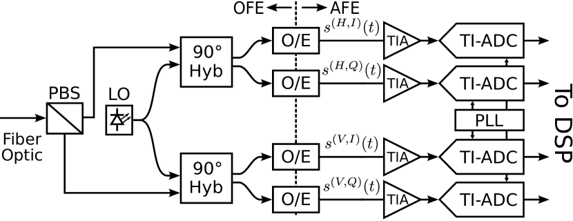
Although the new compensation algorithm proposed in this work can be applied to any high-speed digital communication receiver, to make the discussion more concrete we focus the study on dual-polarization (DP) optical coherent transceivers [1, 2, 3, 4, 5]. A block diagram of an optical front-end (OFE) for a DP coherent receiver is shown in Fig. 1. The optical input signal is decomposed by the OFE to obtain four components, the in-phase and quadrature (I/Q) components of the two polarizations (H/V). The photodetectors convert the optical signals to photocurrents which are amplified by trans-impedance amplifiers (TIAs). The analog front-end (AFE) is in charge of the acquisition and conversion of the electrical signal to the digital domain. Typically, oversampled digital receivers are used to compensate the dispersion experienced in optical links (e.g., where and are the sampling and symbol periods, respectively) [4]. Next we develop the model of the optical channel used in the remainder of this paper.
Let be the -th quadrature amplitude modulation (QAM) symbol in polarization . An optical fiber link with chromatic dispersion (CD) and polarization-mode dispersion (PMD) can be modeled as a multiple-input multiple output (MIMO) complex-valued channel [4] encompassing four complex filters with impulse responses where . Then, the received noise-free electrical signals provided by the optical demodulator can be expressed as [4]
| (1) | ||||
| (2) | ||||
where is the symbol rate and is the optical carrier frequency offset.
II-A Discrete-Time Model of the AFE and the TI-ADC
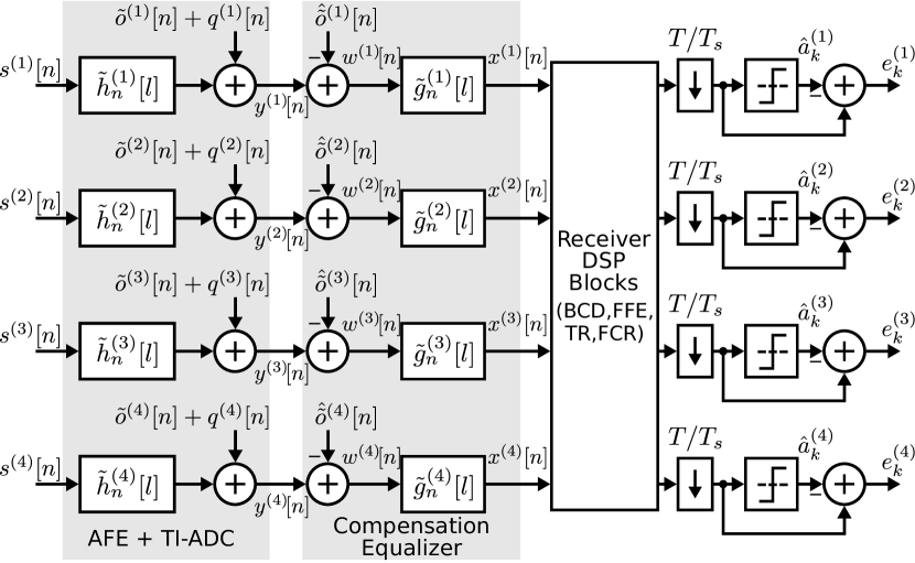
In this section we introduce a discrete-time model for the AFE and TI-ADC system of Fig. 1 including their impairments. A simplified model of the analog path for one component in a given polarization is shown in Fig. 2. Each lane of the AFE includes a filter with impulse response that models the response of the electrical interconnections between the optical demodulator and the TIA, the TIA response itself, and any other components in the signal path up to an -parallel TI-ADC system. Mismatches between and may cause time delay or skew between components and of a given polarization , which degrade the receiver performance. As we shall show here, the proposed background calibration algorithm is able to compensate not only the imperfections of the TI-ADC, but also the I/Q skew and any other mismatches among the signal paths.
The independent frequency responses of the track and hold units in an -channel TI-ADC system are modeled by blocks with . Each -way interleaved TI-ADC path is sampled every seconds with a proper sampling phase. Parameters and model the sampling time errors and the DC offsets, respectively. Path gains are modeled by
| (3) |
where is the gain error.
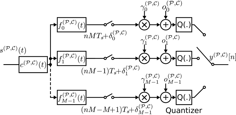
Following [30, 38], the sampling phase error and the path gain are modeled by an analog interpolation filter with impulse response followed by ideal sampling as depicted in Fig. 3. Assuming that the bit-resolution of the ADC’s is sufficiently high, the quantizer can be modeled as additive white noise with uniform distribution. Also, at high-frequency (i.e., ), the offsets generate an -periodic signal denoted as such that with
| (4) |
Then, the digitized high-frequency samples can be expressed as
| (5) |
where is the signal component provided by the -channel TI-ADC, and is the quantization noise (see Fig. 3).
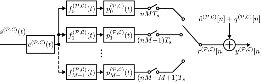
We define the total impulse response of a given subchannel as
| (6) |
where and denotes the convolution operation. Let and be the Fourier transforms (FTs) of and , respectively. In digital communication systems with spectral shaping is for . Further assuming that for , the analog filtering of Fig. 3 can be represented by a real discrete-time model as depicted in Fig. 4 by using
| (7) |
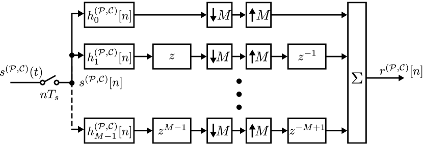
Therefore it can be shown that the digitized high-frequency signal can be expressed as:
| (8) |
where and is the impulse response of a time-varying filter, which is an -periodic sequence such , and defined by
| (9) |
with given by (7)111See [39] and references therein for more details about this formulation.. We highlight that (8) includes the impact of both the AFE mismatches and the -channel TI-ADC impairments. Replacing (8) in (5), the digitized high-frequency sequences result
| (10) |
II-B Compensation of AFE Mismatch and TI-ADC Impairments
Similar to what was done in previous works [30, 38, 39], we propose to use an adaptive digital compensation filter applied after the mitigation of the offset sequence, i.e.,
| (11) |
where is the -periodic time-varying impulse response of the compensation filter (i.e., ), is the number of taps of the compensation filters, and is the offset compensated signal given by
| (12) |
with being the estimated -periodic offset sequence. The combination of the offset compensation blocks and the compensation filters constitutes the Compensation Equalizer (Fig. 5).
A proper strategy to estimate the response of the CE is required. Notice that adaptive calibration techniques based on a reference ADC such as in [39] cannot be used to compensate mismatches between the and signal paths. In the following we propose the backpropagation technique to adapt the CE.
III Error Backpropagation Based Compensation of AFE and TI-ADC Impairments in DP Optical Coherent Receivers
Based on the previous analysis, Fig. 5 depicts a block diagram of the AFE+TI-ADC in a dual-polarization optical coherent receiver with the adaptive calibration block, which includes four instances of the real filter as defined by (11). For simplicity, we modified the notation of the system model of Fig. 4. Note that we use an integer index between 1 and 4 to represent a certain component in a given polarization: , and .
The main receiver functions are included in the digital signal processing (DSP) block of Fig. 5, which works with samples every seconds. In summary, some of the most important DSP algorithms used in these receivers are the chromatic dispersion equalizer (or BCD), the MIMO FFE to compensate the polarization-mode dispersion, Timing Recovery (TR) from the received symbols, the Fine Carrier Recovery (FCR) to compensate the carrier phase and frequency offset, and the Forward Error Correction (FEC) decoder. Readers interested in more details on optical coherent receivers can see [1, 2, 3] and references therein.
III-A All Digital Compensation Architecture
Let with be the filter impulse response in one period defined as
| (13) |
where and is an arbitrary time index multiple of . The filter taps of the CE are adapted by using the slicer error at the output of the receiver DSP block. Let be the slicer error defined by
| (14) |
where is the input of the slicer and is the -th detected symbol at the slicer output (see Fig. 5). Notice that the sampling rate of the slicer inputs is , therefore a subsampling of is carried out after the receiver DSP block. Then, we define the total squared error at the slicer as
| (15) |
Let be the MSE at the slicer with denoting the expectation operator. In this work we use the least mean squares (LMS) algorithm to iteratively adapt the real coefficients of the CE given by (13), in order to minimize the MSE at the slicer:
| (16) |
where ; ; denotes the number of iteration, is the -dimensional coefficient vector at the -th iteration given by
| (17) |
is the adaptation step, and is the gradient of the MSE with respect to the filter vector .
We emphasize that the computation of the MSE gradient is not trivial since is not the error at the output of the CE block. To get the proper error samples to adapt the coefficients of the filters as expressed in (16), we propose the backpropagation algorithm widely used in machine learning [34, 35]. Towards this end, the slicer errors are backpropagated as described in [40]. Finally, based on these backpropagated errors we can estimate the gradient as usual in the classical LMS algorithm.
III-B Error Backpropagation (EBP)
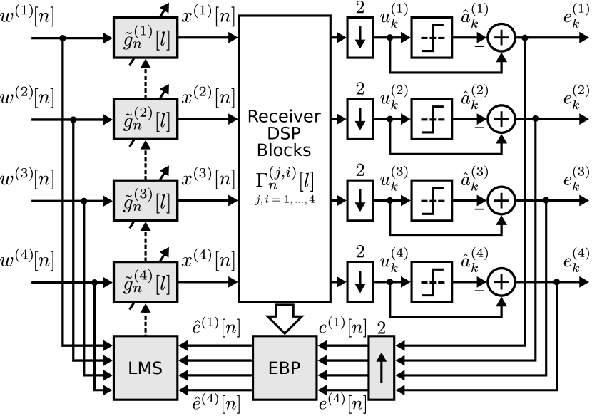
Without loss of generality, we assume that the receiver DSP block can be modeled as a real time-varying MIMO fractional spaced equalizer (i.e., ), which is able to compensate CD and PMD among other optical fiber channel effects. Then, the downsampled output of the receiver DSP block can be written as (see Fig 6)
| (18) |
where is the time-varying impulse response of the filter with input and output , is the number of taps of the filter, while is the signal at the DSP block input given by (11), i.e.,
| (19) |
where is the impulse response defined by (13), denotes the modulo operation, and is the DC compensated signal (12).
As usual with the SGD based adaptation, we replace the gradient of the MSE, , by a noisy estimate, . In the Appendix we show that an instantaneous gradient of the squared error (15) can be expressed as
| (20) |
where is a certain constant, is the -dimensional vector with the samples at the CE input, i.e.,
| (21) |
while is the backpropagated error given by
| (22) |
with being the oversampled slicer error obtained from the baud-rate slicer error in (14) as
| (23) |
Then, a full digital compensation architecture can be derived by using an adaptive CE with
| (24) |
where is the step-size. Furthermore, based on the backpropagated error (22) it is possible to estimate the DC offsets in the input samples as follows
| (25) |
where is the estimate at the -th iteration of the DC offset sequence in one period (see (12)), and is the step-size of the DC offset estimator.
Competition between the CE and any adaptive DSP blocks in (e.g., the FFE) may generate instability, therefore an adaptation constraint must be included. For example, one of the sets of the filter coefficients can be limited to only be a time delay line, for example, where and ( is assumed odd).
Since channel impairments change slowly over time, the coefficient updates given by (24) and (25) do not need to operate at full rate, and subsampling can be applied. The latter allows implementation complexity to be significantly reduced. Additional complexity reduction is enabled by: 1) strobing the algorithms once they have converged, and/or 2) implementing them in firmware in an embedded processor, typically available in coherent optical transceivers. Practical aspects of the hardware implementation shall be discussed in Section V.
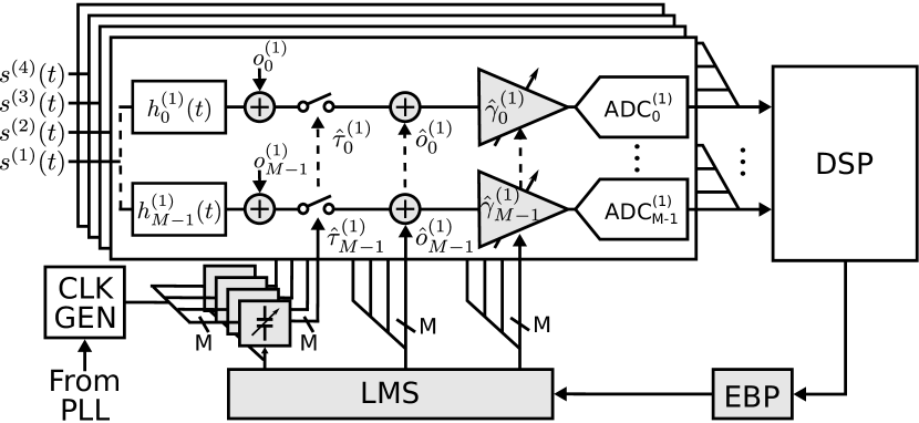
III-C Mixed-Signal Compensation Architecture
A mixed-signal based calibration technique can be also derived from the error backpropagation (EBP) algorithm described in the previous section. Toward this end, sampling phase, gain, and offsets are adjusted before the ADC222Compared to the full-digital compensation architecture, notice that the described mixed-signal solution is not able to compensate some effects such as bandwidth mismatches. by using the gradient of the backpropagated slicer error as depicted in Fig. 7. Similarly to the full digital solution, the DC offsets in the mixed-signal calibration approach are compensated by using (25). The gain is iteratively adjusted by using
| (26) |
where and . Finally, since the backpropagated slicer error is available at the ADC outputs, the sampling phase can be iteratively adjusted by using the MMSE timing recovery algorithm [41], i.e.,
| (27) | ||||
with . The calibration algorithm adjusts analog elements already present in most implementations of the TI-ADC [17, 42, 43]. The clock sampling phase is adjusted with variable delay lines, gain and offset can be corrected in the comparator or with programmable gain amplifiers (PGA), if needed.
IV Simulation Results
| Parameter | Value |
|---|---|
| Modulation | 16-QAM |
| Symbol Rate () | 96 GBd |
| Receiver Oversampling Factor () | 4/3 |
| Fiber Length | 100 km |
| Differential Group Delay (DGD) | 10 ps |
| Second Order Pol. Mode Disp. (SOPMD) | 1000 ps2 |
| Speed of Rotation of the Pol. at the Tx | 2 kHz |
| Speed of Rotation of the Pol. at the Rx | 20 kHz |
| TI-ADC Resolution | 8 bit |
| TI-ADC Sampling Rate (all interleaves) | 128 GS/s |
| Number of Interleaves of TI-ADC () | 16 |
| Number of Taps of CE () | 7 |
| Rolloff Factor | 0.10 |
| Nominal BW of Analog Paths () (see (28)) | 53 GHz |
| Gain Errors (see (3)) - UDRV | |
| Sampling Phase Errors - UDRV | |
| Bandwidth Mismatches (see (28)) - UDRV | |
| I/Q Time Skew (see (29)) - UDRV | |
| DC Offsets - UDRV | VFS |
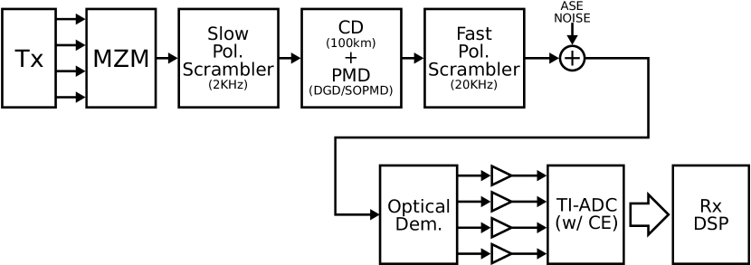
The performance of the proposed backpropagation based adaptive CE is investigated by running Montecarlo simulations of the setup shown in Fig. 8 and defined in Table I. Each test consists of 500 cases where the impairment parameters are obtained by using uniformly distributed random variables (UDRV). The electrical analog path responses (6) are simulated with first-order lowpass filters with 3dB-bandwidth defined by
| (28) |
where is the nominal BW and is the BW mismatch. Let be the mean group delay of the filter of the -th channel and -th component. The impact of the I/Q time skew of polarizations and defined as
| (29) |
with , is also investigated. We consider a 16-QAM modulation scheme with a symbol rate of . Raised cosine filters with rolloff factor for transmit pulse shaping are simulated (i.e., the nominal BW of the channel filters is GHz). The optical signal-to-noise ratio (OSNR) is set to that required to achieve a bit-error-rate (BER) of (see [44, 45] for the definition of OSNR). The oversampling factor in the DSP blocks is . The fiber length is with of differential group delay (DGD) and of second-order PMD (SOPMD). Rotations of the state of polarization (SOP) of and are included at the transmitter and receiver, respectively. TI-ADCs with 8-bit resolution, sampling rate, and are simulated. The number of taps of the digital compensation filters is .
IV-A Montecarlo Simulations of the Adaptive CE
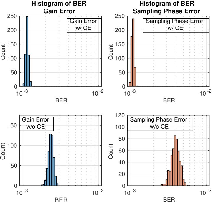
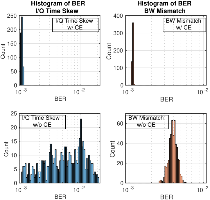
Figs. 9 and 10 show the histograms of the BER for the receiver with and without the CE in the presence of gain errors, phase errors, I/Q time skew, and BW mismatches. Only one effect is exercised in each case. Results of 500 random gain and phase errors uniformly distributed in the interval (see (3)) and , respectively, are depicted in Fig. 9, whereas Fig. 10 shows results for 500 random BW mismatches (see (28)) and I/Q time skews (see (29)) uniformly distributed in the interval and , respectively. In all cases, it is observed that the proposed compensation technique is able to mitigate the impact of all impairments when they are exercised separately333Similar performance has been verified with random DC offsets [37].. In particular, notice that the proposed CE with taps practically eliminates the serious impact on the receiver performance of the I/Q time skew values of Table I.
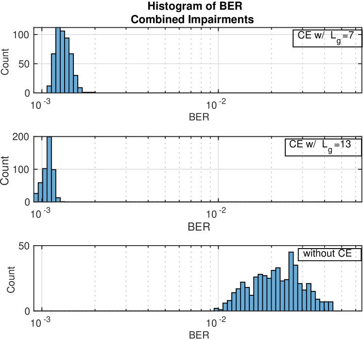
Fig. 11 shows histograms of the BER for the receiver with and without the CE in the presence of the combined effects. Results of 500 cases with random gain errors, sampling phase errors, I/Q time skews, BW mismatches, and DC offsets as defined in Table I, are presented. Performance of the CE with taps is also depicted. As before, note that the CE is able to compensate the impact of all combined impairments. Moreover, note that a slight performance improvement can be achieved when the number of taps increases from 7 to 13.
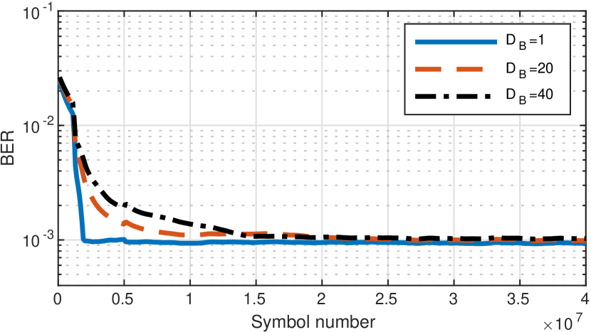
As mentioned in Section III-B, the impairments of the AFE and TI-ADCs change very slowly over time in multi-gigabit optical coherent transceivers. Therefore the coefficient updates given by (24) and (25) do not need to operate at full rate, and subsampling can be applied. Block processing and frequency domain equalization based on the Fast Fourier Transform (FFT) are widely used to implement high-speed coherent optical transceivers [1]. Then we propose to use block decimation of the error samples to update the CE. Let be the block size in samples to be used for implementing the EBP. Define the block decimation factor. In this way, only one block of consecutive samples of the oversampled slicer error (23) every blocks, i.e.,
| (30) |
with integer, is used to adapt the CE. Fig. 12 depicts an example of the temporal evolution of the BER in the presence of combined impairments according to Table I for different values of the block decimation factor with . The instantaneous BER is evaluated every symbols and then processed by a moving average filter of size . Gear shifting is used to accelerate the convergence of the CE and reduce the steady-state MSE. In all cases, notice that the use of block decimation practically does not impact on the resulting BER. Therefore it can be adopted to drastically reduce the implementation complexity, as shall be discussed in Section V.
IV-B Mixed-Signal Compensation of TI-ADC with Highly Interleaved Architectures
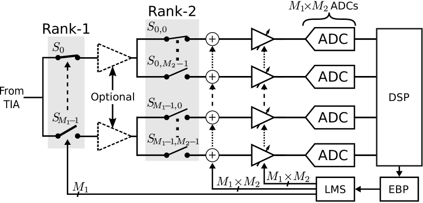
The performance of the mixed-signal scheme of Section III-C is investigated in typical hierarchical ultra high-speed TI-ADCs such as those used in high speed receivers [42, 43, 46]. This hierarchical TI-ADC architecture organizes the T&H in two or more ranks with a high number of sub-ADCs. Fig. 13 depicts an example with two ranks. Rank 1 includes switches each of which feeds T&H stages of Rank 2. Then, ADCs are used to digitize the input signal. Successive approximation register (SAR) ADCs are used for this application due to their power efficiency at the required sampling rate and resolution. This approach relaxes the requirements for the clock generation and synchronization. Furthermore, the impact on the input bandwidth is reduced in contrast to T&H with direct sampling [47]. As an example of application of the mixed-signal compensation scheme of Section III-C, its performance in a hierarchical TI-ADC with and (i.e., individual converters) is evaluated. A clock jitter of RMS is added to this simulation. Notice that the mixed-signal calibration algorithm adjusts the sampling phases of the switches in the first rank, and the gains and offsets of the individual sub-ADCs.
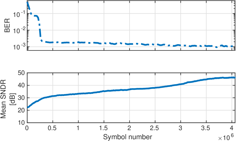
Fig. 14 shows the temporal evolution of both the BER and the mean signal-to-noise-and-distortion-ratio (SNDR) [42]. A slower convergence than the previous simulation is observed as a result of the larger number of converters (i.e., 128 vs 16). Nevertheless, we verify that the proposed backpropagation based mixed-signal compensation scheme is able to mitigate the impact of the impairments in hierarchical TI-ADC. In particular, note that the SNDR can be improved from dB to dB by using the proposed background calibration technique.
V Hardware Complexity Analysis
This section discusses some practical aspects of the implementation of the proposed compensation technique. We focus on the two main blocks of the all digital architecture: the compensation equalizer and the error backpropagation block.
V-A Implementation of the Compensation Equalizer
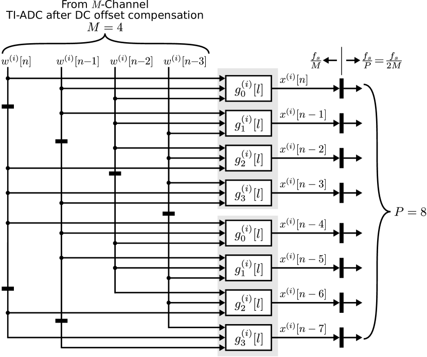
As described in Section III, the compensation equalizer in a DP optical coherent receiver comprises 4 real valued finite impulse response (FIR) filters with , and . From computer simulations of Section IV it was observed that is enough to properly compensate the AFE and TI-ADC impairments. Therefore a time domain implementation is preferred for the CE. Each of these filters has independent impulse responses which are time multiplexed as (see (13)). Note that time multiplexing of filters with independent responses does not translate to additional complexity when the filter is implemented with a parallel architecture. The use of parallel implementation is mandatory in high speed optical communication where parallelism factors on the order of 128 o higher are typical. In these architectures, the parallelism factor can be chosen to be a multiple of the ADC parallelism factor , i.e., where is an integer. Therefore the different time multiplexed coefficients are used in fixed positions of the parallelism without incurring in significant additional complexity in relation to a filter with just one set of coefficients (see Fig. 15). We highlight that the resulting filter is equivalent in complexity to the I/Q-skew compensation filter already present in current coherent receivers [1]. Since the proposed scheme also corrects skew, the classical skew correction filter can be replaced by the proposed CE without incurring significant additional area or power.
V-B Implementation of the Error Backpropagation Block
A straightforward implementation of error backpropagation must include a processing stage for each DSP block located between the ADCs and the slicers. Typically these blocks comprise the BCD, FFE, TR interpolators, and the FCR. All these blocks can be mathematically modeled as a sub-case of the generic receiver DSP block used in Section III-B and the Appendix. The EBP block is algorithmically equivalent to its corresponding DSP block with the only difference that the coefficients are transposed (i.e., compare (36) and (45)). Therefore, in the worst case, the EBP complexity would be similar to that of the receiver DSP block444Note that the LMS adaptation hardware of the FFE, the PLL of the FCR and the PLL of the TR do not need to be implemented in the EBP path, which further reduces the complexity of the latter.. Since doubling power and area consumption is not acceptable for commercial applications, important simplifications must be provided.
Considering that AFE and TI-ADC impairments change very slowly over time in multi-gigabit optical coherent transceivers, the coefficient updates given by (24) and (25) do not need to operate at full rate, and subsampling can be applied. The latter allows implementation complexity, and particularly power dissipation, to be drastically reduced. In Section IV-A we evaluated the performance with block decimation where one block of consecutive samples of the oversampled slicer error are used every blocks. Simulation results not included here have shown a good performance even with and . The block based decimation approach allows the EBP algorithm to be implemented in the frequency domain when necessary to reduce complexity (for example in the EBP of the BCD and FFE). This error decimation reduces the power dissipation of the EBP to only of the power of the corresponding DSP blocks, equivalent to less than 1% in the simulated example. However, the areas of the EBP blocks are still equivalent to the area of their corresponding DSP blocks. To reduce area, the EBP blocks could be implemented using a serial architecture555Typically, a serial implementation requires that hardware such as multipliers be reused with variable numerical values of coefficients, whereas in a parallel implementation hardware can be optimized for fixed coefficient values. This results in a somewhat higher power per operation in a serial implementation. Nevertheless, the drastic power reduction achieved through decimation greatly outweighs this effect. or a lower parallelism factor. If a serial implementation is chosen, an area reduction proportional to the parallelism factor is expected at the expense of increasing the latency by a similar amount. The resulting latency is samples, where and are the block sizes of the FFTs used to implement the BCD and FFE, respectively (factor 2 includes the FFT / IFFT pair). The latencies of the EBP blocks for the TR interpolators and FCR can be neglected. Therefore the CE adaptation speed is not reduced by a serial implementation of the EBP blocks if . Details of efficient architectures for implementing the error backpropagation block will be addressed in a future work.
VI Conclusions
A new TI-ADC background calibration algorithm based on the backpropagation technique has been presented in this paper. Two implementation variants were presented, one of them all-digital and the other mixed-signal. Simulation results have shown a fast, robust and almost ideal compensation/calibration of TI-ADC sampling time, gain, offset, and bandwidth mismatches as well as I/Q time skew effects under different test conditions in the example of application of a DSP-based optical coherent receiver. Hardware complexity is minimized with serial processing and decimation. As the technique runs in background, the calibration can track parameter variations caused by temperature, voltage, aging, etc., without operational interruptions.
Acknowledgements
The authors would like to thank Dr. Ariel Pola for his helpful advice on various technical issues related to the hardware implementation.
Appendix
In this Appendix the stochastic gradient of the squared error defined by (20) is derived. The total squared error (15) is
| (31) |
with given by (18). Define the average squared error as
| (32) |
The derivative of with respect to is
| (33) |
where , , and . From the slicer error given by (14), define the oversampled slicer error as
| (34) |
Thus, (33) can be rewritten as
| (35) |
where is the oversampled compensation equalizer output given by
| (36) |
The time index can be expressed as
| (37) |
with integer. Then, omitting the constant factor , the derivative (35) can be expressed as
| (38) |
Next we evaluate the derivative . Assuming that the DSP filter coefficients do not depend on , from (36) and (37) we verify that
| (39) |
Based on (37), the signal at the DSP block input given by (19) can be rewritten as
| (40) |
Therefore,
| (41) |
where is the Kronecker delta function (i.e., if and if ). Replacing (41) in (39) we get
| (42) |
| (43) | ||||
Finally, we set resulting
| (44) |
where
| (45) |
is the backpropagated error. Notice that (44) is the average of the instantaneous gradient component given by . Therefore, an instantaneous gradient of the square error can be obtained as
| (46) |
where is the -dimensional vector with the samples at the CE input defined by (21).
References
- [1] D. A. Morero, M. A. Castrillón, A. Aguirre, M. R. Hueda, and O. E. Agazzi, “Design Tradeoffs and Challenges in Practical Coherent Optical Transceiver Implementations,” J. Lightw. Technol., vol. 34, no. 1, pp. 121–136, Jan. 2016.
- [2] M. S. Faruk and S. J. Savory, “Digital Signal Processing for Coherent Transceivers Employing Multilevel Formats,” J. Lightw. Technol., vol. 35, no. 5, pp. 1125–1141, Mar. 2017.
- [3] C. R. S. Fludger, “Digital Signal Processing for Coherent Transceivers in Next Generation Optical Networks,” in Proc. Eur. Conf. on Optical Communication (ECOC), Cannes, France, Sep. 2014, pp. 1–3.
- [4] D. E. Crivelli, H. S. Carrer, and M. R. Hueda, “Adaptive Digital Equalization in the Presence of Chromatic Dispersion, PMD, and Phase Noise in Coherent Fiber Optic Systems,” in Proc. IEEE Global Telecommun. Conf., vol. 4, Dallas, TX, USA, Nov. 2004, pp. 2545–2551.
- [5] D. E. Crivelli, M. R. Hueda, H. S. Carrer, M. d. Barco, R. R. López, P. Gianni, J. Finochietto, N. Swenson, P. Voois, and O. E. Agazzi, “Architecture of a Single-Chip 50 Gb/s DP-QPSK/BPSK Transceiver With Electronic Dispersion Compensation for Coherent Optical Channels,” IEEE Trans. Circuits Syst. I, vol. 61, no. 4, pp. 1012–1025, Apr. 2014.
- [6] E. Agrell, M. Karlsson, A. R. Chraplyvy, D. J. Richardson, P. M. Krummrich, P. Winzer, K. Roberts, J. K. Fischer, S. J. Savory, B. J. Eggleton, M. Secondini, F. R. Kschischang, A. Lord, J. Prat, I. Tomkos, J. E. Bowers, S. Srinivasan, M. Brandt-Pearce, and N. Gisin, “Roadmap of optical communications,” J. Opt., vol. 18, no. 6, May 2016.
- [7] K. Roberts, S. H. Foo, M. Moyer, M. Hubbard, A. Sinclair, J. Gaudette, and C. Laperle, “High Capacity Transport—100G and Beyond,” J. Lightw. Technol., vol. 33, no. 3, pp. 563–578, Feb. 2015.
- [8] K. Kikuchi, “Fundamentals of Coherent Optical Fiber Communications,” J. Lightw. Technol., vol. 34, no. 1, pp. 157–179, Jan. 2016.
- [9] G. Bosco, “Advanced Modulation Techniques for Flexible Optical Transceivers: The Rate/Reach Tradeoff,” J. Lightw. Technol., vol. 37, no. 1, pp. 36–49, Jan. 2019.
- [10] C. Laperle and M. OSullivan, “Advances in High-Speed DACs, ADCs, and DSP for Optical Coherent Transceivers,” J. Lightw. Technol., vol. 32, no. 4, pp. 629–643, Feb. 2014.
- [11] L. Kull, D. Luu, P. A. Francese, C. Menolfi, M. Braendli, M. Kossel, T. Morf, A. Cevrero, I. Oezkaya, H. Yueksel, and T. Toifl, “CMOS ADCs Towards 100 GS/s and Beyond,” in Proc. IEEE Compound Semiconductor Integr. Circuit Symp., Austin, TX, USA, Oct. 2016.
- [12] L. Passetti, A. C. Galetto, D. J. Hernando, D. Morero, B. T. Reyes, and M. R. Hueda, “Backpropagation-Based Background Compensation of Frequency Interleaved ADC for Coherent Optical Receivers,” in Proc. IEEE Int. Symp. Circuits Syst., Sevilla Spain, May 2020, pp. 1–5.
- [13] N. Kurosawa, H. Kobayashi, K. Maruyama, H. Sugawara, and K. Kobayashi, “Explicit analysis of channel mismatch effects in time-interleaved ADC systems,” IEEE Trans. Circuits Syst. I, vol. 48, no. 3, pp. 261–271, Mar. 2001.
- [14] C. Vogel, “The Impact of Combined Channel Mismatch Effects in Time-Interleaved ADCs,” IEEE Trans. Instrum. Meas., vol. 54, no. 1, pp. 415–427, Feb. 2005.
- [15] B. Reyes, V. Gopinathan, P. Mandolesi, and M. Hueda, “Joint sampling-time error and channel skew calibration of time-interleaved ADC in multichannel fiber optic receivers,” in Proc. IEEE Int. Symp. Circuits Syst., May 2012, pp. 2981–2984.
- [16] C.-Y. Lin, Y.-H. Wei, and T.-C. Lee, “A 10b 2.6GS/s time-interleaved SAR ADC with background timing-skew calibration,” in Proc. IEEE Int. Solid-State Circuits Conf., San Francisco, CA, USA, Jan. 2016, pp. 468–469.
- [17] B. T. Reyes, R. M. Sanchez, A. L. Pola, and M. R. Hueda, “Design and Experimental Evaluation of a Time-Interleaved ADC Calibration Algorithm for Application in High-Speed Communication Systems,” IEEE Trans. Circuits Syst. I, vol. 64, no. 5, pp. 1019–1030, May 2017.
- [18] M. El-Chammas and B. Murmann, “A 12-GS/s 81-mW 5-bit Time-Interleaved Flash ADC With Background Timing Skew Calibration,” IEEE J. Solid-State Circuits, vol. 46, no. 4, pp. 838–847, Apr. 2011.
- [19] H. Wei, P. Zhang, B. D. Sahoo, and B. Razavi, “An 8 Bit 4 GS/s 120 mW CMOS ADC,” IEEE J. Solid-State Circuits, vol. 49, no. 8, pp. 1751–1761, Aug. 2014.
- [20] J. Song, K. Ragab, X. Tang, and N. Sun, “A 10-b 800-MS/s Time-Interleaved SAR ADC With Fast Variance-Based Timing-Skew Calibration,” IEEE J. Solid-State Circuits, vol. 52, no. 10, pp. 2563–2575, Oct. 2017.
- [21] A. Haftbaradaran and K. Martin, “A Background Sample-Time Error Calibration Technique Using Random Data for Wide-Band High-Resolution Time-Interleaved ADCs,” IEEE Trans. Circuits Syst. II, vol. 55, no. 3, pp. 234–238, 2008.
- [22] J. Elbornsson, F. Gustafsson, and J.-E. Eklund, “Blind equalization of time errors in a time-interleaved ADC system,” IEEE Trans. Signal Process., vol. 53, no. 4, pp. 1413–1424, Apr. 2005.
- [23] A. Salib, B. Cardiff, and M. F. Flanagan, “A Low-Complexity Correlation-Based Time Skew Estimation Technique for Time-Interleaved SAR ADCs,” in Proc. IEEE Int. Symp. Circuits Syst., Baltimore, MD, USA, May 2017, pp. 1–4.
- [24] J. Matsuno, T. Yamaji, M. Furuta, and T. Itakura, “All-Digital Background Calibration Technique for Time-Interleaved ADC Using Pseudo Aliasing Signal,” IEEE Trans. Circuits Syst. I, vol. 60, no. 5, pp. 1113–1121, May 2013.
- [25] S. Devarajan, L. Singer, D. Kelly, T. Pan, J. Silva, J. Brunsilius, D. Rey-Losada, F. Murden, C. Speir, J. Bray, E. Otte, N. Rakuljic, P. Brown, T. Weigandt, Q. Yu, D. Paterson, C. Petersen, J. Gealow, and G. Manganaro, “A 12-b 10-GS/s Interleaved Pipeline ADC in 28-nm CMOS Technology,” IEEE J. Solid-State Circuits, vol. 52, no. 12, pp. 3204–3218, Dec. 2017.
- [26] S. Lee, A. P. Chandrakasan, and H. Lee, “A 1 GS/s 10b 18.9 mW Time-Interleaved SAR ADC With Background Timing Skew Calibration,” IEEE J. Solid-State Circuits, vol. 49, no. 12, pp. 2846–2856, Dec. 2014.
- [27] H. Mafi, M. Yargholi, and M. Yavari, “Digital Blind Background Calibration of Imperfections in Time-Interleaved ADCs,” IEEE Trans. Circuits Syst. I, vol. 64, no. 6, pp. 1504–1514, Jun. 2017.
- [28] A. M. Ali, H. Dinc, P. Bhoraskar, S. Puckett, A. Morgan, Ning Zhu, Qicheng Yu, C. Dillon, B. Gray, J. Lanford, M. McShea, U. Mehta, S. Bardsley, P. Derounian, R. Bunch, R. Moore, and G. Taylor, “A 14-bit 2.5GS/s and 5GS/s RF sampling ADC with background calibration and dither,” in Proc. IEEE Symp. VLSI Circuits, Honolulu, HI, USA, Jun. 2016, pp. 1–2.
- [29] P. Harpe, E. Cantatore, and A. van Roermund, “An oversampled 12/14b SAR ADC with noise reduction and linearity enhancements achieving up to 79.1dB SNDR,” in Proc. IEEE Int. Solid-State Circuits Conf., San Francisco, CA, USA, Feb. 2014, pp. 194–195.
- [30] G. C. Luna, D. E. Crivelli, M. R. Hueda, and O. E. Agazzi, “Compensation of track and hold frequency response mismatches in interleaved analog to digital converters for high-speed communications,” in Proc. IEEE Int. Symp. Circuits Syst., Island of Kos, Greece, May 2006, pp. 1631–1634.
- [31] B. Murmann, “Digitally assisted data converter design,” in Proc. IEEE ESSCIRC 2013, Bucharest, Romania, Sep. 2013, pp. 24–31.
- [32] B. Verbruggen, “Digitally Assisted Analog to Digital Converters,” in High-Performance AD and DA Converters, IC Design in Scaled Technologies, and Time-Domain Signal Processing, P. Harpe, A. Baschirotto, and K. A. A. Makinwa, Eds. Springer International Publishing, 2015, pp. 25–44.
- [33] J. Song and N. Sun, “A 10-b 600-MS/s 2-way Time-Interleaved SAR ADC with Mean Absolute deviation based Background Timing-Skew Calibration,” in Proc. IEEE Custom Integr. Circuits Conf. San Diego, CA: IEEE, Apr. 2018, pp. 1–4.
- [34] D. E. Rumelhart, G. E. Hinton, and R. J. Williams, “Learning representations by back-propagating errors,” Nature, vol. 323, no. 6088, pp. 533–536, Oct. 1986.
- [35] I. Goodfellow, Y. Bengio, and A. Courville, Deep Learning. MIT Press, 2016.
- [36] T. Morie, T. Miki, K. Matsukawa, Y. Bando, T. Okumoto, K. Obata, S. Sakiyama, and S. Dosho, “A 71dB-SNDR 50MS/s 4.2mW CMOS SAR ADC by SNR enhancement techniques utilizing noise,” in Proc. IEEE Int. Solid-State Circuits Conf., San Francisco, CA, Feb. 2013, pp. 272–273.
- [37] F. Solis, A. Fernandez Bocco, D. Morero, M. R. Hueda, B. T. Reyes, and M. R. Hueda, “Background Calibration of Time-Interleaved ADC for Optical Coherent Receivers Using Error Backpropagation Techniques,” in Proc. IEEE Int. Symp. Circuits Syst., May 2020, pp. 1–5.
- [38] O. E. Agazzi, M. R. Hueda, D. E. Crivelli, H. S. Carrer, A. Nazemi, G. Luna, F. Ramos, R. Lopez, C. Grace, B. Kobeissy, C. Abidin, M. Kazemi, M. Kargar, C. Marquez, S. Ramprasad, F. Bollo, V. Posse, S. Wang, G. Asmanis, G. Eaton, N. Swenson, T. Lindsay, and P. Voois, “A 90 nm CMOS DSP MLSD Transceiver With Integrated AFE for Electronic Dispersion Compensation of Multimode Optical Fibers at 10 Gb/s,” IEEE J. Solid-State Circuits, vol. 43, no. 12, pp. 2939–2957, Dec. 2008.
- [39] S. Saleem and C. Vogel, “Adaptive Compensation of Frequency Response Mismatches in High-Resolution Time-Interleaved ADCs using a Low-Resolution ADC and a Time-Varying Filter,” in Proc. IEEE Int. Symp. Circuits Syst., Paris, France, May 2010, pp. 561–564.
- [40] D. A. Morero, M. R. Hueda, and O. E. Agazzi, “Forward and backward propagation methods and structures for coherent optical receiver,” U.S. Patent 10 128 958, Nov., 2018.
- [41] E. A. Lee and D. G. Messerschmitt, Digital Communication, 3rd ed. Dordrecht: Springer, 2004.
- [42] B. T. Reyes, L. Biolato, A. C. Galetto, L. Passetti, F. Solis, and M. R. Hueda, “An Energy-Efficient Hierarchical Architecture for Time-Interleaved SAR ADC,” IEEE Trans. Circuits Syst. I, vol. 66, no. 6, pp. 2064–2076, Jun. 2019.
- [43] L. Kull, D. Luu, C. Menolfi, M. Brändli, P. A. Francese, T. Morf, M. Kossel, A. Cevrero, I. Ozkaya, and T. Toifl, “A 24-72-GS/s 8-b Time-Interleaved SAR ADC With 2.0-3.3-pJ/Conversion and >30 dB SNDR at Nyquist in 14-nm CMOS FinFET,” IEEE J. Solid-State Circuits, vol. 53, no. 12, pp. 3508–3516, Dec. 2018.
- [44] W. Freude, R. Schmogrow, B. Nebendahl, M. Winter, A. Josten, D. Hillerkuss, S. Koenig, J. Meyer, M. Dreschmann, M. Huebner, C. Koos, J. Becker, and J. Leuthold, “Quality metrics for optical signals: Eye diagram, Q-factor, OSNR, EVM and BER,” in Proc. Int. Conf. Transparent Opt. Netw., Jul. 2012, pp. 1–4.
- [45] C. C. K. Chan, Optical Performance Monitoring: Advanced Techniques for Next-Generation Photonic Networks. Academic Press, Feb. 2010.
- [46] G. Kim, M. Kossel, A. Cevrero, I. Ozkaya, A. Burg, T. Toifl, Y. Leblebici, L. Kull, D. Luu, M. Braendli, C. Menolfi, P.-A. Francese, H. Yueksel, C. Aprile, and T. Morf, “A 161-mW 56-Gb/s ADC-Based Discrete Multitone Wireline Receiver Data-Path in 14-nm FinFET,” IEEE J. Solid-State Circuits, vol. 55, no. 1, pp. 38–48, Jan. 2020.
- [47] Y. M. Greshishchev, J. Aguirre, M. Besson, R. Gibbins, C. Falt, P. Flemke, N. Ben-Hamida, D. Pollex, P. Schvan, and S.-C. Wang, “A 40 GS/s 6b ADC in 65nm CMOS,” in Proc. IEEE Int. Solid-State Circuits Conf., Feb. 2010, pp. 390–391.