Granular superconductors for high kinetic inductance and low loss quantum devices
Abstract
Granular aluminum is a promising material for high kinetic inductance devices such as qubit circuits. It has the advantage over atomically disordered materials such as NbNx, to maintain a high kinetic inductance concomitantly with a high quality factor. We show that high quality nano-scale granular aluminum films having a sharp superconducting transition with normal state resistivity values of the order of and kinetic inductance values of the order of can be obtained, surpassing state of the art values. We argue that this is a result of the different nature of the metal-to-insulator transition, being electronic correlations driven (Mott type) in the former and disorder driven (Anderson type) in the latter.
In recent years superconducting (SC) qubit circuits (QC) have evolved considerably. The first type, the so-called Cooper pair box (Bouchiat et al., 1998; Nakamura et al., 1999), was basically composed of an island connected through a small Josephson junction (JJ) to a large pair reservoir, while a voltage V could be applied to it through a gate. States differing by one pair on the island could be weakly coupled through the JJ, creating a two-level system. More recently a different type of qubit, consisting of a small JJ shunted by a high inductance element, was developed to eliminate charge related noise and de-coherence. The large inductance element consisted originally of a one-dimensional array of large size JJ (Mooij et al., 1999; Manucharyan et al., 2009). More recently it was found that it could simply consist of a narrow line of a highly disordered superconductor such as NbNx having a high kinetic inductance thanks to a low superfluid density (Peltonen et al., 2013). Here it is virtual vortex tunneling through the narrow line that is the conjugate of the charge on the junction capacitance. It was however noted that formation of sub-gap states should be avoided in spite of disorder, as such states would introduce dissipation and thus de-coherence. We show here that nano-scale granular superconductors provide better solution because they are close to a Mott transition rather than to an Anderson transition, typical of atomic disorder, which induces a massive presence of sub-gap states.
When the mean free path of a metal is reduced by disorder to be smaller than the BCS coherence length , the superfluid density can be decreased substantially. For a given value of the current, pair velocity is much increased and the kinetic energy of the Cooper pairs becomes the dominant factor of the self-inductance of a stripe.
In a stripe of length , width and thickness the kinetic energy of the superfluid with density and velocity is stored as inductive energy
| (1) |
since and the penetration depth definition is we obtain for the inductance
| (2) |
where is the kinetic inductance divided by the number of squares . Deep in the dirty limit, defined as , , where is the London penetration depth (Tinkham, 2004). Here is the penetration depth in the clean limit where . Using the dirty limit expression for and the BCS relation for where is the Fermi velocity and is the SC gap, and taking into account that where is the relaxation time, we obtain
| (3) |
where is the normal state resistivity. In the BCS weak coupling (Bardeen et al., 1957) one can calculate from the values of the sheet resistance and the critical temperature.
A high inductance can be reached by increasing the value of the sheet resistance. This can be achieved by decreasing the film thickness (for example Nb (Annunziata et al., 2009, 2010)), and/or by using a highly disordered metal such as NbNx (Niepce et al., 2019; Peltonen et al., 2013), NbxSi1-x (le Sueur et al., 2018), TiN (Leduc et al., 2010; Vissers et al., 2010; Swenson et al., 2013; Coumou et al., 2013) and NbTiN (Niepce et al., 2019; Peltonen et al., 2013; le Sueur et al., 2018; Leduc et al., 2010; Vissers et al., 2010; Swenson et al., 2013; Coumou et al., 2013; Samkharadze et al., 2016; Grünhaupt et al., 2018; Maleeva et al., 2018). Because very thin films tend to be discontinuous the inductance values one can reach in this way are rather limited, of the order of a few pH per square (Annunziata et al., 2010). Much higher values, of the order of 1 nH per square, have been reached by using strongly disordered films approaching the metal-to-insulator (M/I) transition, such as NbNx (Peltonen et al., 2013). However it was found out that the quality factor of resonators made of such disordered films tends to deteriorate with disorder (Peltonen et al., 2013). This has so far limited the use of disordered superconducting for high inductance devices, because higher losses mean increased de-coherence effects thus making quantum computing impractical.
Another material that has been considered recently for application in QC is granular aluminum (grAl) (Grünhaupt et al., 2018; Maleeva et al., 2018; Winkel et al., 2019). grAl films can be prepared by thermally evaporating clean aluminum pellets in oxygen environment, for more details see (Moshe et al., 2019). Their structure consists of small grains separated by aluminum oxide insulating barriers. The inter-grain coupling and resulting normal state resistivity are controlled by the oxygen partial pressure and Al deposition rate. High sheet resistance is reached by reducing inter-grain coupling rather than by atomic scale disorder. The phase diagram of vs resistivity has the well known “dome” shape, first rising to reach a maximum value which depends on the temperature of the substrate during film growth (respectively 2.3 K at room temperature (Levy-Bertrand et al., 2019; Deutscher et al., 1973a; Cohen and Abeles, 1968; Dynes et al., 1984), 3 nm grain size (Deutscher et al., 1973a), and 3.2 K at 100 K (Moshe et al., 2019; Bachar et al., 2015, 2013; Pracht et al., 2016, 2017; Deutscher et al., 1973b), 2 nm grain size with a narrower distribution (Deutscher et al., 1973b; Lerer et al., 2014)) and thereafter decreasing as the metal-to-insulator transition is approached.
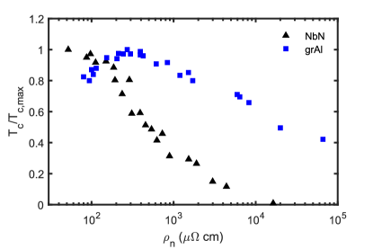
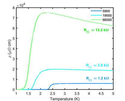
We show in Fig. 1 the decrease of with resistivity of grAl films prepared as described above on liquid nitrogen cooled substrates. This decrease is slow. At a resistivity of is still 40% of its maximum value. By contrast, the of NbNx films collapses much faster. They become useless for device applications at resistivity values of the order of less than . grAl based devices can have kinetic inductance values one order of magnitude higher than NbNx based devices, which represents a considerable advantage. Furthermore, we show in Fig. 2 that the superconductivity transition remains sharp up to the highest resistivity.
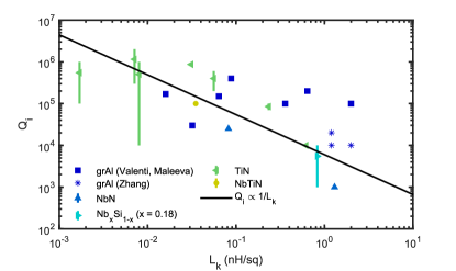
A further critical point concerns the level of losses, as seen for instance in resonators. In Fig. 3 we have collected values of internal quality factors reported for a number of devices as a function of their kinetic inductance values, with the aim of comparing devices based on atomically disordered superconductors such as NbNx with grAl devices (here using films deposited at room temperature (Valenti et al., 2019; Grünhaupt et al., 2018; Maleeva et al., 2018)). The data shows a continuous decrease for the former, and no systematic change for the later. We emphasize that the highest kinetic inductance values reported in this figure are of about 1 . This is because higher values cannot be reached for NbNx and similar atomically disorder films, for the reasons explained above. However, in view of the high quality of our grAl films deposited at liquid nitrogen temperature as shown Fig. 2 we believe that values as high as 10 can be reached without increased losses.
We propose that the origin of the different behaviors of atomically disordered and granular superconductors lies in the different nature of their metal to insulator transition. When disorder is on the atomic scale the transition is of the Anderson type. This is the case in NbNx films where disorder is created by introducing vacancies through a reduction of the nitrogen concentration (Mondal et al., 2011; Chand et al., 2012). The density of states (DOS) of delocalized states decreases progressively to zero as more carriers near the Fermi level become localized. If the metal is a superconductor, the reduced DOS results in a fast decrease of the critical temperature. At the same time the localized carriers create sub-gap states such as two-level systems or collective modes such as the Higgs modes (Sherman et al., 2015) and increased losses must be expected. An increased density of sub-gap states is intrinsic to the vicinity of an Anderson transition.
The nature of the metal-to-insulator transition is quite different in a granular metal consisting of nano-size metal crystallites weakly coupled together. When the coupling is weak enough, the Coulomb charging energy of the grains turns the granular system into an insulator (Abeles, 1977; Beloborodov et al., 2007). By analogy with the Hubbard case (Georges et al., 1996) the transition can be of the Mott type when that energy is of the order of the effective band width of the granular system (determined by the strength of the inter-grain coupling), if disorder effects are not dominant. As discussed by Beloborodov et al., disorder will in fact dominate if the spacing between the electronic levels in the individual grains is small (Beloborodov et al., 2007). The spacing can be approximated by (Kubo, 1962) where is the DOS at the Fermi level and is the grain volume. That spacing is indeed small in the Al-Ge system, in which the grain size is about 10 nm (Gerber et al., 1997). The spacing being then of the order of 1 K. But when the grain size is about 2 nm, the inter-level spacing is about 100 K (Bachar et al., 2020). If, in addition the grain size distribution is narrow as is the case here, a Mott transition can be preserved. Indeed, disorder appears to play in that case only a minor role since superconductivity persists up to values smaller than unity! (Moshe et al., 2019). Additional experimental evidence for a Mott transition in nano-scale grAl has been previously presented and discussed (Bachar et al., 2015).
| Material | t (nm) | |||
|---|---|---|---|---|
| grAl (Valenti et al., 2019) | 20 | 20 | 0.016* | |
| grAl (Valenti et al., 2019) | 40 | 20 | 0.032* | |
| grAl (Valenti et al., 2019) | 80 | 20 | 0.064* | |
| grAl (Valenti et al., 2019) | 110 | 20 | 0.088* | |
| grAl (Valenti et al., 2019) | 450 | 20 | 0.360* | |
| grAl (Valenti et al., 2019) | 800 | 20 | 0.640* | |
| grAl (Grünhaupt et al., 2018; Maleeva et al., 2018) | 2000 | 20 | ~ | 2 |
| grAl (Zhang et al., 2019) | 1645 | 26 | 1.2 | |
| grAl (Zhang et al., 2019) | 1661 | 25 | 1.2 | |
| grAl (Zhang et al., 2019) | 2706 | 37 | 2 | |
| NbNx (Niepce et al., 2019) | 500 | 20 | 0.082* | |
| NbNx (Peltonen et al., 2013) | 2000 | 2-3 | 1.3 | |
| NbxSi1-x (x=0.18) (le Sueur et al., 2018) | 600 | 15 | 0.83 | |
| TiN (Leduc et al., 2010; Vissers et al., 2010) | 25 | 40 | ~ | 0.008* |
| TiN (Swenson et al., 2013) | 45 | 22 | 0.031* | |
| TiN (Coumou et al., 2013) | 600 | 6 | ~ | 0.620 |
| TiN (Shearrow et al., 2018) | 505 | 8.9 | 0.234* | |
| TiN (Shearrow et al., 2018) | 145 | 14.2 | 0.056* | |
| TiN (Shearrow et al., 2018) | 21 | 49.8 | 0.0071* | |
| TiN (Shearrow et al., 2018) | 6 | 109 | 0.0017* | |
| NbTiN (Samkharadze et al., 2016) | 250 | 8 | ~ | 0.035* |
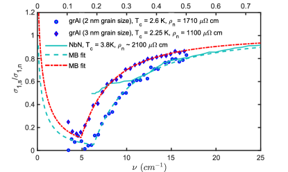
In Fig. 4 we compare the optical conductivity versus frequency of the two systems for similar values of the resistivity. In high resistivity NbNx samples the real part of the conductivity remains high below the gap value obtained from a fit to Mattis-Bardeen (MB) theory (Mattis and Bardeen, 1958) at high frequencies, indicating the massive presence of in-gap states. This deviation from MB is systematic for high resistivity low NbNx films (Sherman et al., 2015; Cheng et al., 2016). In strong contrast, in high resistivity grAl samples the fit to MB theory remains good down to low frequencies, for both grain sizes. The data for 3 nm grain size sample has been taken by us with the same setup as described in (Moshe et al., 2019). The density of sub-gap states, if present, is evidently much lower than in NbNx. The good agreement with the MB theory is in line with the measured temperature dependence of the change in resonance frequency for a series of resonators made of grAl, with resistvities up to , deposited onto substrates held at room temperature (Valenti et al., 2019).
The internal quality factor can be approximated by the expression which holds for thin film and a kinetic induction fraction of order unity (Coumou et al., 2013). At frequencies below the gap, and in the zero temperature limit the value of is expected to approach zero for (the data in Fig. 4 was taken at ~0.6-0.7 for grAl and ~0.4 for NbNx) (Mattis and Bardeen, 1958). Therefore, the presence of sub-gap states for NbNx suggests that a lower quality factor would be obtained than for grAl. A difference by two orders of magnitude in the quality factors as can be seen in Table 1 between grAl and NbNx having a similar sheet resistance of 2000 Ω is therefore reasonable.
On the basis of these compared optical conductivity data we expect higher losses in devices based on NbNx, and other atomically disordered superconductors, than in devices using nano-scale grAl. This is borne out by the respective quality factor values of resonators made of these two types of materials, see Table 1. In atomically disordered superconductors the quality factor decreases as the sheet resistance and the related inductance increase, while resonators made of grAl have both a high inductance and a high quality factor.
Regarding the possibility of other Mott granular SC, we suggest granular materials having a level spacing of the order of 100 K. The advantage of grAl is that this criterion is established naturally during the sample evaporation, without any need for expensive techniques. Al-Ge films deposited at low temperature are also a possibility (Fontaine and Meunier, 1972).
In summary, we suggest that the nature of the M/I transition is crucial for achieving both high kinetic inductance and high quality factor devices. Atomically disordered SC are less suitable for this purpose, as evident from the low quality factors which we believe result from massive presence of sub-gap states seen from optical conductivity data. In contrast, nano-scale superconductors, such as grAl, are more suitable for this purpose. Their higher quality factor at large kinetic inductance values results we believe from the absence of intrinsic sub-gap states. We have interpreted this difference as being due to the different nature of the metal-to-insulator transition in these two systems, being of the Anderson type in NbNxand of the Mott type in nano-scale grAl. We suggest therefore that high inductance devices based on superconducting granular films, consisting of grains of only a few nano-meters with a narrow size distribution so as to reduce disorder effects, should be further considered for implementation in quantum circuits.
We acknowledge fruitful discussions with Ioan Pop, Florence Levy-Bertrand, Marc Scheffler, Nimrod Bachar and Christoph Strunk, held at the Superconducting Kinetic Inductances 2019 workshop in Bad Honnef, hosted by the Wilhelm and Else Heraeus-Foundation.
DATA AVAILABILITY
The data that supports the findings of this study are available within the article.
References
- Bouchiat et al. (1998) V. Bouchiat, D. Vion, P. Joyez, D. Esteve, and M. H. Devoret, Physica Scripta T76, 165 (1998).
- Nakamura et al. (1999) Y. Nakamura, Y. A. Pashkin, and J. S. Tsai, Nature 398, 786 (1999).
- Mooij et al. (1999) J. E. Mooij, T. P. Orlando, L. Levitov, L. Tian, C. H. van der Wal, and S. Lloyd, Science 285, 1036 (1999), https://science.sciencemag.org/content/285/5430/1036.full.pdf .
- Manucharyan et al. (2009) V. E. Manucharyan, J. Koch, L. I. Glazman, and M. H. Devoret, Science 326, 113 (2009), https://science.sciencemag.org/content/326/5949/113.full.pdf .
- Peltonen et al. (2013) J. T. Peltonen, O. V. Astafiev, Y. P. Korneeva, B. M. Voronov, A. A. Korneev, I. M. Charaev, A. V. Semenov, G. N. Golt’sman, L. B. Ioffe, T. M. Klapwijk, and J. S. Tsai, Phys. Rev. B 88, 220506 (2013).
- Tinkham (2004) M. Tinkham, Introduction to Superconductivity: Second Edition, Dover Books on Physics (Dover Publications, 2004).
- Bardeen et al. (1957) J. Bardeen, L. N. Cooper, and J. R. Schrieffer, Physical Review 108, 1175 (1957).
- Annunziata et al. (2009) A. J. Annunziata, D. F. Santavicca, J. D. Chudow, L. Frunzio, M. J. Rooks, A. Frydman, and D. E. Prober, IEEE Transactions on Applied Superconductivity 19, 327 (2009).
- Annunziata et al. (2010) A. J. Annunziata, D. F. Santavicca, L. Frunzio, G. Catelani, M. J. Rooks, A. Frydman, and D. E. Prober, Nanotechnology 21, 445202 (2010).
- Niepce et al. (2019) D. Niepce, J. Burnett, and J. Bylander, Phys. Rev. Applied 11, 044014 (2019).
- le Sueur et al. (2018) H. le Sueur, A. Svilans, N. Bourlet, A. Murani, L. Bergé, L. Dumoulin, and P. Joyez, arXiv e-prints , arXiv:1810.12801 (2018), arXiv:1810.12801 [cond-mat.supr-con] .
- Leduc et al. (2010) H. G. Leduc, B. Bumble, P. K. Day, B. H. Eom, J. Gao, S. Golwala, B. A. Mazin, S. McHugh, A. Merrill, D. C. Moore, O. Noroozian, A. D. Turner, and J. Zmuidzinas, Applied Physics Letters 97, 102509 (2010), https://doi.org/10.1063/1.3480420 .
- Vissers et al. (2010) M. R. Vissers, J. Gao, D. S. Wisbey, D. A. Hite, C. C. Tsuei, A. D. Corcoles, M. Steffen, and D. P. Pappas, Applied Physics Letters 97, 232509 (2010), https://doi.org/10.1063/1.3517252 .
- Swenson et al. (2013) L. J. Swenson, P. K. Day, B. H. Eom, H. G. Leduc, N. Llombart, C. M. McKenney, O. Noroozian, and J. Zmuidzinas, Journal of Applied Physics 113, 104501 (2013), https://doi.org/10.1063/1.4794808 .
- Coumou et al. (2013) P. C. J. J. Coumou, M. R. Zuiddam, E. F. C. Driessen, P. J. de Visser, J. J. A. Baselmans, and T. M. Klapwijk, IEEE Transactions on Applied Superconductivity 23, 7500404 (2013).
- Samkharadze et al. (2016) N. Samkharadze, A. Bruno, P. Scarlino, G. Zheng, D. P. DiVincenzo, L. DiCarlo, and L. M. K. Vandersypen, Phys. Rev. Applied 5, 044004 (2016).
- Grünhaupt et al. (2018) L. Grünhaupt, N. Maleeva, S. T. Skacel, M. Calvo, F. Levy-Bertrand, A. V. Ustinov, H. Rotzinger, A. Monfardini, G. Catelani, and I. M. Pop, Phys. Rev. Lett. 121, 117001 (2018).
- Maleeva et al. (2018) N. Maleeva, L. GrÃŒnhaupt, T. Klein, F. Levy-Bertrand, O. Dupre, M. Calvo, F. Valenti, P. Winkel, F. Friedrich, W. Wernsdorfer, A. V. Ustinov, H. Rotzinger, A. Monfardini, M. V. Fistul, and I. M. Pop, Nature Communications 9, 3889 (2018).
- Winkel et al. (2019) P. Winkel, K. Borisov, L. Grünhaupt, D. Rieger, M. Spiecker, F. Valenti, A. V. Ustinov, W. Wernsdorfer, and I. M. Pop, arXiv e-prints , arXiv:1911.02333 (2019), arXiv:1911.02333 [quant-ph] .
- Moshe et al. (2019) A. G. Moshe, E. Farber, and G. Deutscher, Phys. Rev. B 99, 224503 (2019).
- Levy-Bertrand et al. (2019) F. Levy-Bertrand, T. Klein, T. Grenet, O. Dupré, A. Benoît, A. Bideaud, O. Bourrion, M. Calvo, A. Catalano, A. Gomez, J. Goupy, L. Grünhaupt, U. v. Luepke, N. Maleeva, F. Valenti, I. M. Pop, and A. Monfardini, Phys. Rev. B 99, 094506 (2019).
- Deutscher et al. (1973a) G. Deutscher, H. Fenichel, M. Gershenson, E. Grunbaum, and Z. Ovadyahu, Journal of Low Temperature Physics 10, 231 (1973a).
- Cohen and Abeles (1968) R. W. Cohen and B. Abeles, Phys. Rev. 168, 444 (1968).
- Dynes et al. (1984) R. C. Dynes, J. P. Garno, G. B. Hertel, and T. P. Orlando, Phys. Rev. Lett. 53, 2437 (1984).
- Bachar et al. (2015) N. Bachar, S. Lerer, A. Levy, S. Hacohen-Gourgy, B. Almog, H. Saadaoui, Z. Salman, E. Morenzoni, and G. Deutscher, Physical Review B 91, 041123 (2015).
- Bachar et al. (2013) N. Bachar, S. Lerer, S. Hacohen-Gourgy, B. Almog, and G. Deutscher, Physical Review B 87, 214512 (2013).
- Pracht et al. (2016) U. S. Pracht, N. Bachar, L. Benfatto, G. Deutscher, E. Farber, M. Dressel, and M. Scheffler, Physical Review B 93, 100503 (2016).
- Pracht et al. (2017) U. S. Pracht, T. Cea, N. Bachar, G. Deutscher, E. Farber, M. Dressel, M. Scheffler, C. Castellani, A. M. GarcÃa-GarcÃa, and L. Benfatto, Physical Review B 96, 094514 (2017).
- Deutscher et al. (1973b) G. Deutscher, M. Gershenson, E. Grunbaum, and Y. Imry, Journal of Vacuum Science and Technology 10, 697 (1973b).
- Lerer et al. (2014) S. Lerer, N. Bachar, G. Deutscher, and Y. Dagan, Physical Review B 90, 214521 (2014).
- Mondal et al. (2011) M. Mondal, A. Kamlapure, M. Chand, G. Saraswat, S. Kumar, J. Jesudasan, L. Benfatto, V. Tripathi, and P. Raychaudhuri, Phys. Rev. Lett. 106, 047001 (2011).
- Valenti et al. (2019) F. Valenti, F. Henriques, G. Catelani, N. Maleeva, L. Grünhaupt, U. von Lüpke, S. T. Skacel, P. Winkel, A. Bilmes, A. V. Ustinov, J. Goupy, M. Calvo, A. Benoît, F. Levy-Bertrand, A. Monfardini, and I. M. Pop, Phys. Rev. Applied 11, 054087 (2019).
- Chand et al. (2012) M. Chand, G. Saraswat, A. Kamlapure, M. Mondal, S. Kumar, J. Jesudasan, V. Bagwe, L. Benfatto, V. Tripathi, and P. Raychaudhuri, Phys. Rev. B 85, 014508 (2012).
- Sherman et al. (2015) D. Sherman, U. S. Pracht, B. Gorshunov, S. Poran, J. Jesudasan, M. Chand, P. Raychaudhuri, M. Swanson, N. Trivedi, A. Auerbach, M. Scheffler, A. Frydman, and M. Dressel, Nature Physics 11, 188 (2015).
- Abeles (1977) B. Abeles, Physical Review B 15, 2828 (1977).
- Beloborodov et al. (2007) I. S. Beloborodov, A. V. Lopatin, V. M. Vinokur, and K. B. Efetov, Rev. Mod. Phys. 79, 469 (2007).
- Georges et al. (1996) A. Georges, G. Kotliar, W. Krauth, and M. J. Rozenberg, Rev. Mod. Phys. 68, 13 (1996).
- Kubo (1962) R. Kubo, Journal of the Physical Society of Japan 17, 975 (1962).
- Gerber et al. (1997) A. Gerber, A. Milner, G. Deutscher, M. Karpovsky, and A. Gladkikh, Phys. Rev. Lett. 78, 4277 (1997).
- Bachar et al. (2020) N. Bachar, A. Levy, T. Prokscha, A. Suter, E. Morenzoni, Z. Salman, and G. Deutscher, Phys. Rev. B 101, 024424 (2020).
- Zhang et al. (2019) W. Zhang, K. Kalashnikov, W.-S. Lu, P. Kamenov, T. DiNapoli, and M. Gershenson, Phys. Rev. Applied 11, 011003 (2019).
- Shearrow et al. (2018) A. Shearrow, G. Koolstra, S. J. Whiteley, N. Earnest, P. S. Barry, F. J. Heremans, D. D. Awschalom, E. Shirokoff, and D. I. Schuster, Applied Physics Letters 113, 212601 (2018), https://doi.org/10.1063/1.5053461 .
- Cheng et al. (2016) B. Cheng, L. Wu, N. J. Laurita, H. Singh, M. Chand, P. Raychaudhuri, and N. P. Armitage, Phys. Rev. B 93, 180511 (2016).
- Mattis and Bardeen (1958) D. C. Mattis and J. Bardeen, Phys. Rev. 111, 412 (1958).
- Fontaine and Meunier (1972) A. Fontaine and F. Meunier, Physik der kondensierten Materie 14, 119 (1972).