Broadband, millimeter-wave anti-reflective structures on sapphire ablated with femto-second laser
Abstract
We designed, fabricated, and measured anti-reflection coating (ARC) on sapphire that has 116% fractional bandwidth and transmission of at least 97% in the millimeter wave band. The ARC was based on patterning pyramid-like sub-wavelength structures (SWS) using ablation with a 15 W femto-second laser operating at 1030 nm. One side of each of two discs was fabricated with SWS that had a pitch of 0.54 mm and height of 2 mm. The average ablation volume removal rate was 1.6 mm3/min. Measurements of the two-disc sandwich show transmission higher than 97% between 43 and 161 GHz. We characterize instrumental polarization (IP) arising from differential transmission due to asymmetric SWS. We find that with proper alignment of the two disc sandwich RMS IP across the band is predicted to be 0.07% at normal incidence, and less than 0.6% at incidence angles up to 20 degrees. These results indicate that laser ablation of SWS on sapphire and on other hard materials such as alumina is an effective way to fabricate broad-band ARC.
I Introduction
Sapphire, alumina, and silicon have material properties that make them appealing for use as optical elements in the millimeter and sub-millimeter (MSM) waveband, loosely defined as 30 - 3000 GHz. Compared to plastic-based materials, they have indices of refraction near 3, giving more aberration correction power per unit lens thickness Lamb . They have amongst the lowest absorption loss at room temperature and when cooled to cryogenic temperatures parshin1995 , and they have thermal conductance higher by factors of hundreds, making them useful for cryogenic applications child_1973 . Sapphire has 10% birefringence making it an ideal half-wave plate (HWP) material for polarimetric applications. A number of astrophysical instruments operating in the MSM waveband are using these materials Thornton_2016 ; EBEX2018 ; SPT-3G ; Kaneko2020 .
The high index of refraction leads to high reflection loss; the average reflectance across 30% fractional bandwidth of a 1 cm thick slab of non-birefringent sapphire at 150 GHz is 40%. Reduction of reflection loss is achieved by applying an anti-reflection coating (ARC). There are two generic approaches for implementing ARC: (i) applying layers of materials with appropriately chosen intermediate indices; and (ii) machining sub-wavelength structures (SWS) on the native optical element material Raut2011AntireflectiveCA .
An advantage of the SWS approach is that it does not require new materials and glues. This advantage matches well the needs of cryogenic instruments in which differences in coefficients of thermal expansion make the application of multi-layers challenging. Another advantage is that SWS give flexibility in synthesizing any index profile between free space and the substrate material. Prescriptions exist for index profiles that give fractional bandwidths exceeding 100% with maximal, in some sense optimal, in-band transmission Klopfenstein .
Two classes of MSM instruments that require broad-bandwidths and cryogenic optical elements are those mapping the spatial polarization of the cosmic microwave background radiation (CMB)Johnson_2007 ; EBEX2018 ; SPT-3G ; Simon2018 ; Kaneko2020 ; SO-OverviewGalitzki10.1117/12.2312985 ; cmb-s4techbookfirsted , and others measuring the properties of Galactic dust Dober_blastpol10.1117/12.2054419 ; blasttngLourie10.1117/12.2314396 ; nika2pisano2020 . A number of these instruments have used, or plan to use, a sapphire-based HWP polarization modulator. To reduce detector noise the HWP is maintained at cryogenic temperatures, typically near 4 K, and to increase instrument throughput a single HWP operates over a broad range of frequencies, making a single quarter-wave layer of ARC inadequate. Examples of relevant past instruments include BLASTpol and EBEX, which had sapphire HWPs with operating bandwidth of 69% and 109%, respectivelyDober_blastpol10.1117/12.2054419 ; EBEX2018 . The bandwidth of the EBEX HWP is the largest reported to date. Ongoing and future experiments include POLARBEAR2, Simons Observatory and LiteBIRDKaneko2020 ; SO-OverviewGalitzki10.1117/12.2312985 ; sugai .
LiteBIRD is a Japanese-led space mission scheduled to be launched late in the next decade sugai ; YSakurai . LiteBIRD’s low frequency telescope (LFT), designed to operate between 34 and 161 GHz (a fractional bandwidth of 130%), will have an aperture diameter of 40 cm with a HWP operating at 20 K. Currently no ARC technology on sapphire is available over this broad bandwidth. Implementing SWS ARC for the LiteBIRD HWP has motivated the developments we report in this paper.
Although SWS have advantages as ARC, their implementation on hard materials such as sapphire and alumina present fabrication challenges Araujo2016 ; JAIN20021269 ; TUERSLEY1994377 ; machining_difficult . Broad bandwidths require SWS with aspect ratios – defined as height/pitch – reaching four. Diameters of anticipated sapphire and alumina optical elements, which are reaching 80 cmAliCPTHong10.1093/nsr/nwy019 , require commercially viable machining speed. To overcome these challenges we demonstrated a technique to fabricate mm-wave SWS on sapphire, alumina, and silicon using laser micro-fabrication tomo ; karl ; victor ; tomo_ISSTT . With laser ablation, which has already been used in the past to ablate these and other materials Bonse2002 ; Ihlemann1995 ; WANG2004221 , there is no wear and tear of the machining tool. Even for materials that can be machined using conventional tools, laser ablation gives finer control of structure shapes, because laser spot diameters can be focused to smaller sizes than other tools. A spot diameter of 16 m has been demonstrated at the IR HSakurai ; smaller spot diameters are achievable in the UV. Finer control of SWS shapes would give higher transmission over broader bandwidth.
Schütz et al. and Matsumura et al. (Refs. victor, ; tomo, ) demonstrated laser-ablated aspect ratios 2.2 and 2.5 and heights between 700 and 800 m, with sapphire and alumina, respectively. Young et al. (Ref. karl, ) extended the technique to silicon, showing with height near 700 m. To demonstrate applicability to lower frequencies and broader bandwidths, Matsumura et al. (Ref. tomo_ISSTT, ) fabricated structures with and total height of 2.1 mm on sapphire. In all of these cases, the volume ablation rate was small, making fabrication of large samples prohibitively expensive; for example, at the rate Matsumura et al. (Ref. tomo_ISSTT, ) quoted for the 2.1 mm tall structures on sapphire it would have taken two months to fabricate a 10 cm diameter sample. Further steps in the development of laser micro-fabrication of mm-wave SWS include demonstrating ablation rates that would make commercial fabrication viable with SWS aspect ratios suitable for broad bandwidth applications wen_inprep . In this paper we present progress in the design, fabrication, and characterization of laser-ablated SWS ARC, aiming for 130% fractional bandwidth ARC centered on 97 GHz with improved fabrication speed. In Section II, we present the design of the SWS. Sections III and IV give details of the fabrication of two sapphire samples and their transmission properties. We discuss the results and give conclusions in Sections V and VI.
II Design
LiteBIRD’s LFT, one of three telescopes aboard the spacecraft sugai , will operate over a frequency range between 34 and 161 GHz. The focal plane will have about 1200 bolometric detectors tuned to nine broad-band, 25% fractional bandwidth frequency bands. A single HWP placed at the entrance aperture of the LFT will modulate the polarization of sky signals across the entire bandwidth. Thus, the goal is to demonstrate SWS ARC with 130% fractional bandwidth centered on 97 GHz.
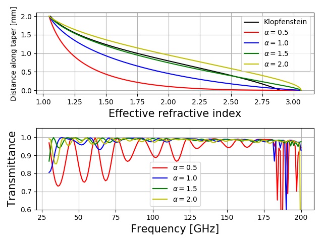
Klopfenstein (Ref. Klopfenstein, ) derived a prescription for impedance matching between free space and a sample of index . The prescription gives an optimal index of refraction profile and depends on a parameter that controls the trade-off between the lowest frequency of the passband and transmission ripple in-band Grann . All values of between 0.01 and 0.1 give average band transmission between 98% and 99%, and we chose as a fiducial value. With this value average transmission is near 99%. There are several approaches to transforming the index profile to a physical shape but there is no single closed-form solution Grann ; Chen:95 . We employ an empirical design approach: we construct physical shapes and use effective medium theory (EMT) EMT and rigorous coupled-wave analysis (RCWA) 1457488 ; Moharam to calculate the resulting index profile. We choose the physical shape that most closely reproduces the desired Klopfenstein index profile. RCWA calculations were carried out using DiffractMOD diffractmod .
We model the SWS as a grid of identical pyramids, see Figure 1. We search for a pyramid shape that closely matches the Klopfenstein index profile by constructing a shape function that gives the width of the pyramid as a function of distance from the substrate material
| (1) |
where the parameters are defined in Figure 1. A value of gives linear slopes; smaller (larger) values give concave (convex) slopes. We considered several values for , but in all cases used mm and mm, giving . The pitch is set by requiring that at normal incidence the smallest value of the highest pass-band frequency be GHz. Thus mm, where is the index of c-cut sapphire. Smaller value of implies shorter , higher , and thus larger bandwidth. In Section V.2 we discuss non-normal incidence. Guidance for the minimum required is obtained by considering the lowest pass-band frequency and applying the standard criterion for maximum transmission with a single ARC layer that has a uniform index . In that case , and the thickness of the layer should be , where is the vacuum wavelength. For the pyramids we found empirically that should satisfy mm, where mm. We required mm. The choice of was determined iteratively by trying several values. We determined that mm is the largest value that would still give an effective index that matches the Klopfenstein profile. Larger values produce a mismatch of the indices near . We assumed that the deep laser ablated grooves will give making (see Figure 1).
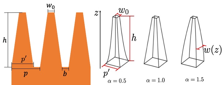
We used second-order EMT to calculate the effective index of refraction as a function of , and RCWA to calculate the expected transmission as a function of frequency; see Figure 2. A convex pyramid shape with gives an index profile that closely matches the Klopfenstein profile with the fiducial . The average band transmissions for and 2 are 97.7%, 98.4%, and 98.3%, respectively; see Figure 2. The sharp reflection features apparent in the Figure above 180 GHz are due to the onset of diffraction.
III Sample Preparation and characterization
III.1 Sapphire
We procured three samples of c-cut sapphire that were cut from the same ingot, each mm thick and 100 mm diameter. We used one sample and the apparatus discussed in Section IV to measure the index of refraction and loss and obtained and , which is consistent with other data Lamb . In subsequent analysis and simulations we assume that these values are common to all three samples.
We fabricated the SWS on a circular area of 34.5 mm diameter on one side of each of two samples, to which we refer as Sample 1 and Sample 2. We patterned only one side because LiteBIRD’s LFT HWP will be a Pancharatnam multi-stack achromatic HWP Pancharatnam1 with SWS only on the outermost surfaces. In Section IV we present transmission measurements of each sample and when they are stacked flat side on flat side.
Using c-cut, non-birefringent sapphire, simplifies interpretation of the results. At normal incidence, which is the only experimental data we present here, any apparent birefringence is the result of asymmetry in fabrication, not of inherent asymmetry in the material, as would be the case with birefringent a-cut sapphire.
III.2 Laser machining
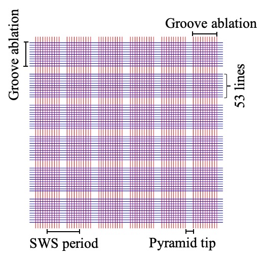
The SWS are patterned using a 15 W average power femto-second laser operating at 1030 nm; the laser parameters are given in Table 1. The laser beam scans lines in two orthogonal directions to make grooves, and thus produce the pyramids; see Figure 3. This scan strategy largely follows an approach we used in the past, see for example Young et al. (Ref karl, ). The focus position is set at a fixed mm throughout the ablation. The surface of the disk at the beginning of ablation is at and negative values are inside the sample.
| Model: Pharos, PH1-15W | |
|---|---|
| Wavelength | 1030 nm |
| Repetition rate | 75 kHz |
| Pulse duration | 290 fs |
| Pulse energy | 200 J |
| Spot diameter () | 15.5 m |
III.3 Characterization of fabricated structures
The SWS were imaged using confocal imaging. A three-dimensional image of a section of the fabricated region is shown in Figure 4. Visual inspection indicates that all SWS are physically intact with no breakage nor damaged tips. We measured 160 structures at each of five locations in each sample, in the center and in four edge regions, and quantified several geometrical parameters as detailed in Figure 4 and Table 2. Values given in the Table are averages and standard deviations of the 800 measurements. We established a global cartesian coordinate system that was aligned with the grooves, and for each measured pyramid we defined and planes that intersected the center of its peak. For both planes (and for each pyramid) we quantified the widths and and two ‘saddle’ heights and , which quantified the depths between pyramids in the and directions. The total height is given by the depth into trenches in the diagonal direction where the laser beam ablates in both the and passes. We best-fit the slopes of the pyramids as imprinted in the and planes to produce measured and .
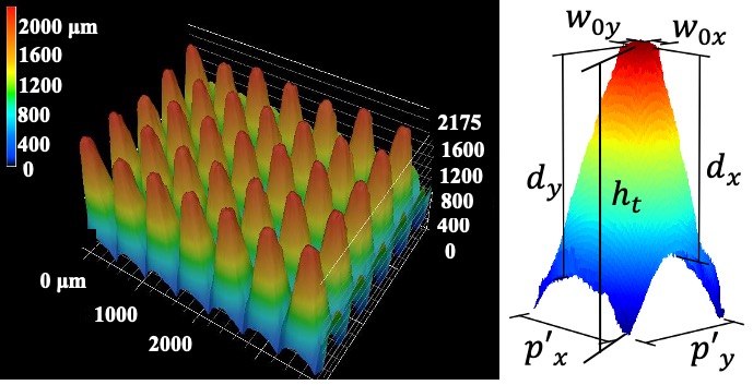
There is good agreement between the design and fabricated values for the pitch and total height, and there is - symmetry in the measured pitch. There is good repeatability between the two samples, which were fabricated several days apart. Asymmetry of 5%-20% is apparent at the tip of the structures, the saddle heights, and the slope values . This structural asymmetry could have been caused by laser beam polarization, which was not monitored; by the ablation scan strategy, for example the order in which and directions were scanned; or by laser beam projection, if the sample was not precisely normal to the beam.
It took 10.5 hours to fabricate each sample giving an average volume removal rate (AVRR) of 1.6 mm3/min. This rate is 18 times faster than achieved in one of our earlier publications tomo_ISSTT . The higher rate is due to using five times higher averaged power and a more efficient sample scan pattern. Matsumura et al. (Ref. tomo, ) report a higher AVRR of 2.2 mm3/min, but with higher power (25 W) and for SWS with smaller total height of 715 m; Schuetz et al. (Ref. victor, ) show that AVRR increases with power and lower structure height.
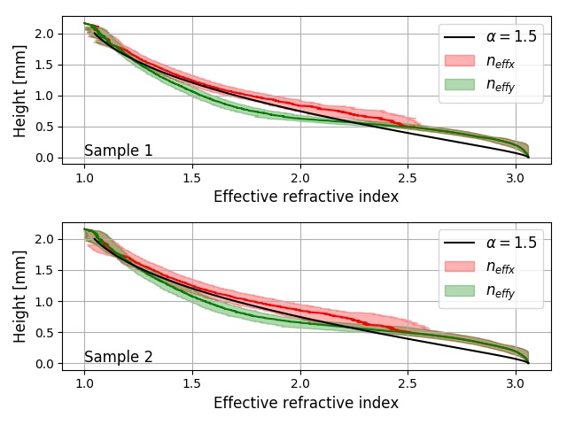
Using EMT and the average values given in Table 2 we calculated effective index profiles in and for each sample; see Figure 5. To indicate the variance we included the index profiles for all 800 measured structures as shaded regions. As the values in Table 2 indicate, the measured profiles in match the design profile with better than the measured profiles in .
| Parameter | Design value | Sample 1 | Sample 2 |
|---|---|---|---|
| (mm) | (mm) | (mm) | |
| Top width () | 0.1 | ||
| Top width () | 0.1 | ||
| Saddle height () | |||
| Saddle height () | |||
| Total height () | 2.0 | ||
| Pitch () | 0.54 | ||
| Pitch () | 0.54 | ||
| † | 1.5 | ||
| † | 1.5 | ||
| † dimensionless quantity | |||
IV Transmission
We measured the transmittance of the samples at normal incidence between 33 and 190 GHz. The apparatus, a schematic of which is shown in Figure 6, consisted of a source of microwaves, an optical chopper operating at 30 Hz, two parabolic mirrors, a diode detector, and a lock-in amplifier. Between the two mirrors there was an aperture of 30 mm diameter, a sample holder, attenuators to reduce standing waves, and two always identically aligned wire grid polarizers with calculated efficiency exceeding 99% across the bandwidth. The transmission axis of the polarizers was aligned to within 3 degrees with the axis of the samples, and the stacked samples were aligned relative to each other to within 0.5 degrees.
To further reduce the effects of standing waves our reported transmittance at each frequency is the average of two transmission measurements taken with the detector positioned at two locations spaced by along the light path. Each transmission measurement is the ratio of power detected with the sample to the power detected without it.
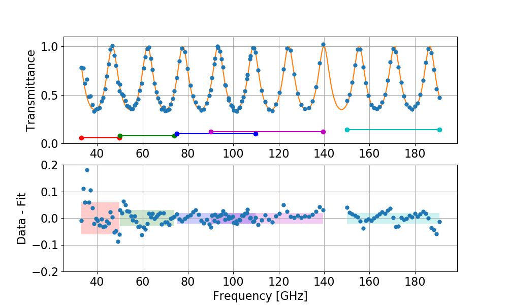
Measurements of transmission through one of the native samples establish error estimates for subsequent data analysis. We measured transmission using different RF sources at five sub-bands between 33 and 190 GHz; see the top panel of Figure 7. We fit the transmittance to a model with two free parameters, the index of refraction and loss tangent, and find the residuals; see the bottom panel of Figure 7. We identify systematic residuals as arising from incomplete cancellation of standing waves and quote the RMS of the residual as the error of transmission measurements in each sub-band. They are 6% (33-50 GHz), 3% (50-75 GHz), and 2% (75-190 GHz).
The errors quoted in Section III.1 for the values of the index of refraction and loss were derived by fitting the transmittance data using statistical errors with magnitude per band as given above and including uncertainty on the measurement of sample thickness. The index and loss errors are dominated by the thickness measurement uncertainty.

We measured the transmittance of each sample and of both mechanically attached flat-side to flat-side. The two samples were held together; no glue was used. The samples were stacked with orientations aligned parallel to each other. Each of the measurements was conducted with the transmission axis of the wire grid polarizers parallel and perpendicular to the axis of the samples. We refer to these measurements as and , respectively, indicating that the incident and measured polarization states align with the and orientations of the samples. The measurements are shown in Figure 8 together with the predicted transmission, which was calculated using RCWA and was based on the average values given in Table 2 and no loss. The transmittances and of individual samples agree with predictions and are only 0.75 because they were patterned only on one side.
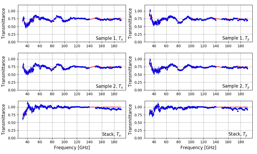
For the stacked samples we find 91% transmittance averaged between the and data for the lowest LiteBIRD frequency band between 34 and 46 GHz. For the second lowest band between 43 and 58 GHz the average is 97%. Other frequency bands have above 98% averaged transmittance. At frequencies above 150 GHz the transmittance of the stack is decreasing and is lower than predicted. An analysis using data over the entire bandwidth (33-190 GHz) and varying the loss tangent in the fit model gives a minimum for , which is consistent with measurements with the native sample.
While determining the precise cause of lower transmittance at higher frequencies is beyond the scope of this paper, we discuss several candidates. Calculations indicate that a uniform 30 m air gap between the stacked samples could explain the observed feature. Measurements set an upper limit of 24 m. Ruze scattering from a flat surface with 30 m RMS roughness could decrease transmittance to 95% at 180 GHz 1446714 . This roughness value is close to the 30 m uncertainty we quote for SWS height measurements (see Table 2), which could be interpreted as an effective roughness. However, transmission measurements of the single samples indicate lower levels of effective roughness. Evidently, any such higher loss is not sufficiently prominent to be exhibited with significant signal-to-noise ratio with transmission measurements of the individual samples. A combination of these effects could be the cause of the lower transmission.
V Systematic Effects
Systematic asymmetry in fabrication along the two orthogonal axes, due to laser beam polarization or birefringent material properties (if such is used), leads to different effective indices of refraction along the two axes. Differential index causes differential transmission, which is a source of instrumental polarization (IP), the conversion of unpolarized to polarized light by the optical element. Even when the structures are two-dimensional symmetric there is differential reflection at non-normal incidence, as there would with any ARC scheme; differences in transmission between S and P polarization states of the incident light lead to IP.
To quantify the IP induced by normal incidence differential transmission we use the figure of merit radio_astronomy ; karl
| (2) | ||||
| (3) |
where we have introduced in the last expression the relative rotation angle between the orientation of the sample and the direction along which transmission is probed. IP vanishes for normal incidence light when the substrate and ARC are -projected isotropic. At normal incidence Equations 2 and 3 could have been written equivalently in terms of and , the transmissions for S and P polarization states.
At non-normal incidence and in the presence of - ARC asymmetry and depend on both the angle of incidence and on the azimuthal angle of the plane of incidence, measured relative to . We now have
| (4) |
see Figure 9.
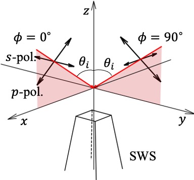
In Secs. V.1 and V.2, we quantify systematic effects due to asymmetry in the fabricated SWS at normal incidence (Section V.1) and due to non-normal incidence (Section V.2), and discuss the level of mitigation provided by appropriately stacking the two-disc sandwich. We refer to ‘parallel’ and ‘perpendicular’ configurations, in which the two plates are stacked with their axes parallel, or with of one perpendicular to of the other, respectively. In the perpendicular configuration the quantities and refer to transmission measurements relative to the axis of the source-side sample of the stack, which was Sample 1.
V.1 Asymmetry of SWS at normal incidence
Figure 10 shows IP inferred from the measured data (Figure 8) for the individual samples and when stacked in the parallel and perpendicular configurations. It also shows the calculated response (using RCWA) using the average parameters for the and orientations in Table 2. We find values of IP reaching 10% at frequencies below 100 GHz for the individual samples, and below 50 GHz for the parallel stacking. For the entire bandwidth the RMS IP is 2.5%. At frequencies higher than 50 GHz, IP in the parallel stacking configuration is smaller than in the individual samples because of higher transmission and because of some averaging of the two somewhat different asymmetries. However, when the plates are stacked in the perpendicular configuration we find lower IP across the band as shown in the bottom panel of Figure 10. The data and the RCWA prediction are consistent within measurement errors, which take into account residual standing waves (see Section IV). If the errors are assumed to be statistical, we find an upper limit of 1% on the RMS across the band. The RMS IP calculated based on RCWA is 0.07%, a value that is nearly 35 times smaller than in the parallel configuration, and is below our measurement limits.
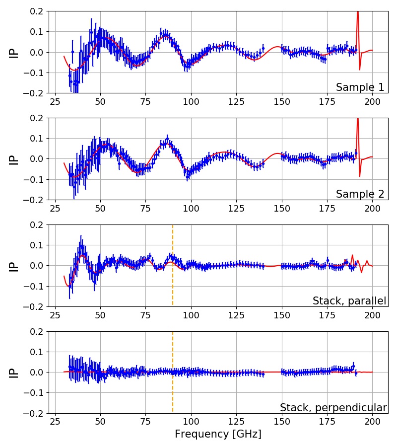
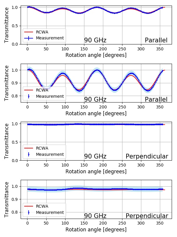
Figure 11 gives data and RCWA predictions for normal incidence transmittance as a function of stacked sample rotation angle for the two configurations at 90 GHz. Concentrating on the parallel configuration first, the effective differential index in and is an effective stack birefringence that causes 8.6% modulation as a function of with periodicity only with fully polarized incident light. That is, the measurements, which were conducted with fully polarized light, give
| (5) |
with , GHz, and indicates that we average all values at the indicated and with periodicity. If the experiment and simulation were conducted with partially polarized or unpolarized light, this -periodic modulation would have diminished or vanished, respectively. For the HWP, SWS using a-cut sapphire, effect also could vanish with unpolarized light. Given measurement errors in this band of frequencies as shown in Figure 7, the -periodic modulation of 0.086 has an uncertainty of 0.014.
The IP signal due to differential transmission has periodicity. Given the measurement uncertainty the data only give a upper limit of IP , when calculated using Equation 3. This value is consistent with the IP value at 90 GHz in the third panel of Figure 10, . This level would persist if the measurement was done with unpolarized light. In the perpendicular configuration both the and -periodic modulation amplitudes, calculated using Equations 5 and 3, are consistent with zero within measurement errors.
The transmission data as a function of , such as presented in Figure 11, reveal that measurements at only two orientations and as shown in Figure 10 and IP calculated using Equation 2 combine information from distinct physical effects. The effects correspond to, and can be quantified with higher accuracy using decomposition to Fourier harmonicsHanany:05 ; kkomatsu . We fit the data of Figure 11 to the model
| (6) |
and constrain the amplitudes and phases. We find IP and , in the parallel and perpendicular configurations, respectively; and and , respectively, for the effect of stack birefringence. The data in the perpendicular configuration is consistent with zero we thus quote an upper limit of 0.5% on the values of and . We find that (1) the and periodic modulations quantified through and are more tightly constrained compared to using Equations 3 and 5; (2) the modulation amplitude constraints calculated using the two techniques are consistent; (3) there is a significant detection of IP, that is, periodic modulation, in the parallel case but not in the perpendicular case; and (4) the relatively large 7.9% periodic modulation measured in the parallel case is not detectable in the perpendicular case.
With the structures as fabricated, perpendicular stacking is predicted to constrain IP to below 0.5% at 90 GHz, a value that is limited by measurement uncertainty, not by inherent asymmetry.
V.2 Non-normal incident light
Optical systems are designed to admit rays over a range of incidence planes and angles and thus calculations of systematic effects arising from ARC SWS asymmetry should take account of the entire range of incidence planes and angles. Including the full range amounts to averaging that gives smaller systematic effects compared to using a single incidence plane and the extreme incidence angle. In the discussion below we analyze the effects of non-normal incidence angles without any such averaging, and therefore the quantitative values should be understood as upper limits. The analysis relies solely on RCWA calculations of the perpendicular configuration; we have already established that this configuration has smaller level of systematic effects.
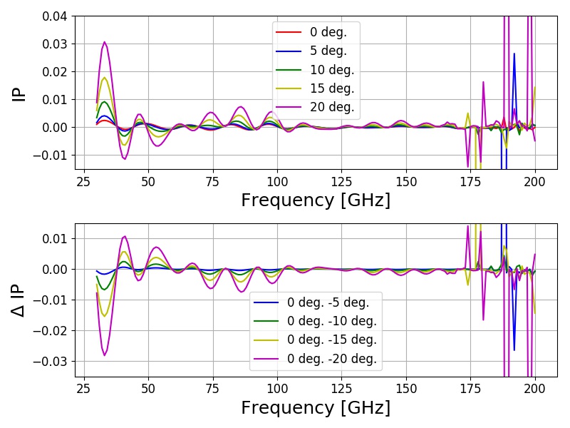
The upper panel of Figure 12 shows calculated IP as a function of frequency for normal incidence and for the 5, 10, 15 and 20 degrees incidence angle. For normal incidence the calculation is identical to the one shown in the lower panel in Figure 10. The lower panel shows the difference between transmission at normal incidence and at other angles, again for . For LiteBIRD’s maximum planned incidence angle of 15 degrees RMS IP across the band is 0.4%, an increase of 0.3% relative to normal incidence. At 20 degrees incidence, RMS IP increases to 0.6%. For degrees, RMS IP values at 15 and 20 degrees incidence are smaller by 0.1%.
Onset of diffraction is apparent at lower frequencies with larger incidence angles. For non-normal incidence, the frequency of diffraction onset – that is, at the lowest order – is Grann ; Bruckner:07
| (7) |
providing qualitative agreement with the RCWA calculation. We do not expect exact quantitative agreement because the RCWA calculation assumes the full average shape information for the two samples, as given in Table 2, whereas Equation 7 only assumes a periodic array of scattering centers.
VI Conclusions
SWS have advantages as ARC because they obviate the need for multiple materials and glues with precisely tuned indices of refraction, and because the index gradient produced can be smoother and tailored to specific applications. SWS are superior for cryogenic applications, because there is no need to match materials with different coefficients of thermal expansion. Fabricating SWS on alumina and sapphire – materials that have favorable optical properties in the millimeter and sub-millimeter wave band – using standard machining approaches has been challenging because both materials are among the hardest available. They rank 9/10 on the relative hardness Mohs scale, and sapphire (alumina) has a value of 2500 (2000) HV on the Vickers hardness scale. In this paper we have extended our development of laser ablation as a tool to fabricate SWS for the millimeter and sub-millimeter band. We demonstrated structures on sapphire with aspect ratio . The newly fabricated SWS give a working bandwidth of 130% with transmission above 90% centered on 97 GHz, and of 116% with transmission of at least 97% centered on 102 GHz, arguably the largest bandwidths yet demonstrated in this wavelength range.
Using shorter pulse duration higher power laser and a more efficient fabrication process we have accelerated the AVRR for sapphire by a factor of 18 to 1.6 mm3/min. Further acceleration is achievable with increase in laser power Neuenschwander ; boerner2019 and improvements in fabrication efficiency.
Although the native material was non-birefringent we found shape asymmetries in the fabricated SWS. The origin of the asymmetries is yet to be understood. However, calculations show that proper relative alignment of samples reduces the magnitude of induced instrumental polarization due to differential reflection by a factor of 35 to 0.07% at normal incidence, and to less than 0.6% for incidence angles up to 20 degrees. Measurements at normal incidence are consistent with these predictions as they show the expected reduction in instrumental polarization, but are currently limited to an upper limit of 1%.
These results and newer ones showing even higher ablation rates indicate that laser ablation of SWS on sapphire and on other hard materials such as alumina is an effective way to fabricate broad-band ARC; the technique has particularly strong advantages in the case of cryogenic applications.
Acknowledgements.
We acknowledge the World Premier International Research Center Initiative (WPI), MEXT, Japan for support through Kavli IPMU. This work was supported by JSPS KAKENHI Grant Numbers JP17H01125, 19K14732, 18J20148, 18KK0083, and JSPS Core-to-Core Program, A. Advanced Research Networks. This work was also supported by the New Energy and Industrial Technology Development Organization (NEDO) project “Development of advanced laser processing with intelligence based on high-brightness and high efficiency laser technologies” by Council for Science, Technology and Innovation (CSTI), Cross-ministerial Strategic Innovation Promotion Program (SIP), “Photonics and Quantum Technology for Society 5.0” and by the Center of Innovation Program, from Japan Science and Technology Agency, JST.DATA AVAILABILITY
The data that support the findings of this study are available from the corresponding author upon reasonable request.
References
- (1) James W. Lamb. Miscellaneous data on materials for millimetre and submillimetre optics. International Journal of Infrared and Millimeter Waves, 17(12):1997–2034, Dec 1996.
- (2) V. V. Parshin, R. Heidinger, B. A. Andreev, A. V. Gusev, and V. B. Shmagin. Silicon as an advanced window material for high power gyrotrons. International Journal of Infrared and Millimeter Waves, 16(5):863–877, May 1995.
- (3) Gregg E. Childs, Lewis J. Ericks, and Robert L. Powell. Thermal Conductivity of Solids At Toom Temperature and Below. Monogram. 131. U.S. Department of commerce, 1973. National Bureau of Standards Boulder Colorado 80302 september.
- (4) R. J. Thornton, P. A. R. Ade, S. Aiola, F. E. Angilè, M. Amiri, J. A. Beall, D. T. Becker, H-M. Cho, S. K. Choi, P. Corlies, K. P. Coughlin, R. Datta, M. J. Devlin, S. R. Dicker, R. Dünner, J. W. Fowler, A. E. Fox, P. A. Gallardo, J. Gao, E. Grace, M. Halpern, M. Hasselfield, S. W. Henderson, G. C. Hilton, A. D. Hincks, S. P. Ho, J. Hubmayr, K. D. Irwin, J. Klein, B. Koopman, Dale Li, T. Louis, M. Lungu, L. Maurin, J. McMahon, C. D. Munson, S. Naess, F. Nati, L. Newburgh, J. Nibarger, M. D. Niemack, P. Niraula, M. R. Nolta, L. A. Page, C. G. Pappas, A. Schillaci, B. L. Schmitt, N. Sehgal, J. L. Sievers, S. M. Simon, S. T. Staggs, C. Tucker, M. Uehara, J. van Lanen, J. T. Ward, and E. J. Wollack. THE ATACAMA COSMOLOGY TELESCOPE: THE POLARIZATION-SENSITIVE ACTPol INSTRUMENT. The Astrophysical Journal Supplement Series, 227(2):21, dec 2016.
- (5) Asad M. Aboobaker, Peter Ade, Derek Araujo, François Aubin, Carlo Baccigalupi, Chaoyun Bao, Daniel Chapman, Joy Didier, Matt Dobbs, Christopher Geach, Will Grainger, Shaul Hanany, Kyle Helson, Seth Hillbrand, Johannes Hubmayr, Andrew Jaffe, Bradley Johnson, Terry Jones, Jeff Klein, Andrei Korotkov, Adrian Lee, Lorne Levinson, Michele Limon, Kevin MacDermid, Tomotake Matsumura, Amber D. Miller, Michael Milligan, Kate Raach, Britt Reichborn-Kjennerud, Ilan Sagiv, Giorgio Savini, Locke Spencer, Carole Tucker, Gregory S. Tucker, Benjamin Westbrook, Karl Young, and Kyle Zilic. The EBEX balloon-borne experiment—optics, receiver, and polarimetry. The Astrophysical Journal Supplement Series, 239(1):7, nov 2018.
- (6) J. Sobrin, P. Ade, Z. Ahmed, A. J. Anderson, J. Avva, R. Basu Thakur, A. Bender, B. Benson, J. Carlstrom, F. Carter, T. Cecil, C. Chang, J. Ding, A. Harke-Hosemann, J. Henning, T. Khaire, S. Kuhlmann, V. Novosad, J. Pearson, C. Posada, G. Wang, and V. Yefremenko. Design and characterization of the SPT-3G receiver. In 2018 SPIE Astronomical Telescopes and Instrumentation (Austin, TX, US, 06/10/2018 - 06/15/2018), volume 10708, pages – ,. Millimeter, Submillimeter, and Far-Infrared Detectors and Instrumentation for Astronomy IX, 2018, 10.1117/12.2314366.
- (7) Daisuke Kaneko, S. Adachi, P. A. R. Ade, M. Aguilar Faúndez, Y. Akiba, K. Arnold, C. Baccigalupi, D. Barron, D. Beck, S. Beckman, F. Bianchini, D. Boettger, J. Borrill, J. Carron, S. Chapman, K. Cheung, Y. Chinone, K. Crowley, A. Cukierman, M. Dobbs, R. Dűnner, H. El-Bouhargani, T. Elleflot, J. Errard, G. Fabbian, S. M. Feeney, C. Feng, T. Fujino, N. Galitzki, A. Gilbert, N. Goeckner-Wald, J. Groh, G. Hall, N. W. Halverson, T. Hamada, M. Hasegawa, M. Hazumi, C. A. Hill, L. Howe, Y. Inoue, G. Jaehnig, O. Jeong, N. Katayama, B. Keating, R. Keskitalo, S. Kikuchi, T. Kisner, N. Krachmalnicoff, A. Kusaka, A. T. Lee, D. Leon, E. Linder, L. N. Lowry, A. Mangu, F. Matsuda, Y. Minami, M. Navaroli, H. Nishino, J. Peloton, A. T. P. Pham, D. Poletti, G. Puglisi, C. L. Reichardt, C. Ross, Y. Segawa, M. Silva-Feaver, P. Siritanasak, N. Stebor, R. Stompor, A. Suzuki, O. Tajima, S. Takakura, S. Takatori, D. Tanabe, G. P. Teply, T. Tomaru, C. Tsai, C. Verges, B. Westbrook, and Y. Zhou. Deployment of polarbear-2a. Journal of Low Temperature Physics, 199(3):1137–1147, May 2020.
- (8) Hemant K. Raut, V. Anand Ganesh, Appukuttan Sreekumaran Nair, and Seeram Ramakrishna. Anti-reflective coatings: A critical, in-depth review. Number 4, pages 3779–3804. Energy Environ. Sci.
- (9) R. W. Klopfenstein. A transmission line taper of improved design. Proceedings of the IRE, 44(1):31–35, Jan 1956.
- (10) B. R. Johnson, J. Collins, M. E. Abroe, P. A. R. Ade, J. Bock, J. Borrill, A. Boscaleri, P. de Bernardis, S. Hanany, A. H. Jaffe, T. Jones, A. T. Lee, L. Levinson, T. Matsumura, B. Rabii, T. Renbarger, P. L. Richards, G. F. Smoot, R. Stompor, H. T. Tran, C. D. Winant, J. H. P. Wu, and J. Zuntz. MAXIPOL: Cosmic microwave background polarimetry using a rotating half-wave plate. The Astrophysical Journal, 665(1):42–54, aug 2007.
- (11) S. M. Simon, J. A. Beall, N. F. Cothard, S. M. Duff, P. A. Gallardo, S. P. Ho, J. Hubmayr, B. J. Koopman, J. J. McMahon, F. Nati, M. D. Niemack, S. T. Staggs, E. M. Vavagiakis, and E. J. Wollack. The advanced actpol 27/39 ghz array. Journal of Low Temperature Physics, 193(5):1041–1047, Dec 2018.
- (12) Nicholas Galitzki, Aamir Ali, Kam S. Arnold, Peter C. Ashton, Jason E. Austermann, Carlo Baccigalupi, Taylor Baildon, Darcy Barron, James A. Beall, Shawn Beckman, Sarah Marie M. Bruno, Sean Bryan, Paolo G. Calisse, Grace E. Chesmore, Yuji Chinone, Steve K. Choi, Gabriele Coppi, Kevin D. Crowley, Kevin T. Crowley, Ari Cukierman, Mark J. Devlin, Simon Dicker, Bradley Dober, Shannon M. Duff, Jo Dunkley, Giulio Fabbian, Patricio A. Gallardo, Martina Gerbino, Neil Goeckner-Wald, Joseph E. Golec, Jon E. Gudmundsson, Erin E. Healy, Shawn Henderson, Charles A. Hill, Gene C. Hilton, Shuay-Pwu Patty Ho, Logan A. Howe, Johannes Hubmayr, Oliver Jeong, Brian Keating, Brian J. Koopman, Kenji Kiuchi, Akito Kusaka, Jacob Lashner, Adrian T. Lee, Yaqiong Li, Michele Limon, Marius Lungu, Frederick Matsuda, Philip D. Mauskopf, Andrew J. May, Nialh McCallum, Jeff McMahon, Federico Nati, Michael D. Niemack, John L. Orlowski-Scherer, Stephen C. Parshley, Lucio Piccirillo, Mayuri Sathyanarayana Rao, Christopher Raum, Maria Salatino, Joseph S. Seibert, Carlos Sierra, Max Silva-Feaver, Sara M. Simon, Suzanne T. Staggs, Jason R. Stevens, Aritoki Suzuki, Grant Teply, Robert Thornton, Calvin Tsai, Joel N. Ullom, Eve M. Vavagiakis, Michael R. Vissers, Benjamin Westbrook, Edward J. Wollack, Zhilei Xu, and Ningfeng Zhu. The Simons Observatory: instrument overview. In Jonas Zmuidzinas and Jian-Rong Gao, editors, Millimeter, Submillimeter, and Far-Infrared Detectors and Instrumentation for Astronomy IX, volume 10708, pages 1 – 13. International Society for Optics and Photonics, SPIE, 2018.
- (13) Maximilian H. Abitbol et al. CMB-S4 Collaboration. Cmb-s4 technology book, first edition, 2017.
- (14) Bradley J. Dober, Peter A. R. Ade, Peter Ashton, Francesco E. Angilè, James A. Beall, Dan Becker, Kristi J. Bradford, George Che, Hsiao-Mei Cho, Mark J. Devlin, Laura M. Fissel, Yasuo Fukui, Nicholas Galitzki, Jiansong Gao, Christopher E. Groppi, Seth Hillbrand, Gene C. Hilton, Johannes Hubmayr, Kent D. Irwin, Jeffrey Klein, Jeff Van Lanen, Dale Li, Zhi-Yun Li, Nathan P. Lourie, Hamdi Mani, Peter G. Martin, Philip Mauskopf, Fumitaka Nakamura, Giles Novak, David P. Pappas, Enzo Pascale, Fabio P. Santos, Giorgio Savini, Douglas Scott, Sara Stanchfield, Joel N. Ullom, Matthew Underhill, Michael R. Vissers, and Derek Ward-Thompson. The next-generation BLASTPol experiment. In Wayne S. Holland and Jonas Zmuidzinas, editors, Millimeter, Submillimeter, and Far-Infrared Detectors and Instrumentation for Astronomy VII, volume 9153, pages 137 – 148. International Society for Optics and Photonics, SPIE, 2014.
- (15) Nathan P. Lourie, Peter A. R. Ade, Francisco E. Angile, Peter C. Ashton, Jason E. Austermann, Mark J. Devlin, Bradley Dober, Nicholas Galitzki, Jiansong Gao, Sam Gordon, Christopher E. Groppi, Jeffrey Klein, Gene C. Hilton, Johannes Hubmayr, Dale Li, Ian Lowe, Hamdi Mani, Philip Mauskopf, Christopher M. McKenney, Federico Nati, Giles Novak, Enzo Pascale, Giampaolo Pisano, Adrian Sinclair, Juan D. Soler, Carole Tucker, Joel N. Ullom, Michael Vissers, and Paul A. Williams. Preflight characterization of the BLAST-TNG receiver and detector arrays. In Jonas Zmuidzinas and Jian-Rong Gao, editors, Millimeter, Submillimeter, and Far-Infrared Detectors and Instrumentation for Astronomy IX, volume 10708, pages 52 – 66. International Society for Optics and Photonics, SPIE, 2018.
- (16) A. Monfardini C. Tucker P.A.R. Ade A. Shitvov A. Benoit M. Calvo A. Catalano J. Goupy S. Leclercq J. Macias-Perez A. Andrianasolo N. Ponthieu G. Pisano, A. Ritacco. Development and application of metamaterial-based half-wave plates for the nika and nika2 polarimeters, 2020.
- (17) H. Sugai, P. A. R. Ade, Y. Akiba, D. Alonso, K. Arnold, J. Aumont, J. Austermann, C. Baccigalupi, A. J. Banday, R. Banerji, R. B. Barreiro, S. Basak, J. Beall, S. Beckman, M. Bersanelli, J. Borrill, F. Boulanger, M. L. Brown, M. Bucher, A. Buzzelli, E. Calabrese, F. J. Casas, A. Challinor, V. Chan, Y. Chinone, J.-F. Cliche, F. Columbro, A. Cukierman, D. Curtis, P. Danto, P. de Bernardis, T. de Haan, M. De Petris, C. Dickinson, M. Dobbs, T. Dotani, L. Duband, A. Ducout, S. Duff, A. Duivenvoorden, J.-M. Duval, K. Ebisawa, T. Elleflot, H. Enokida, H. K. Eriksen, J. Errard, T. Essinger-Hileman, F. Finelli, R. Flauger, C. Franceschet, U. Fuskeland, K. Ganga, J.-R. Gao, R. Génova-Santos, T. Ghigna, A. Gomez, M. L. Gradziel, J. Grain, F. Grupp, A. Gruppuso, J. E. Gudmundsson, N. W. Halverson, P. Hargrave, T. Hasebe, M. Hasegawa, M. Hattori, M. Hazumi, S. Henrot-Versille, D. Herranz, C. Hill, G. Hilton, Y. Hirota, E. Hivon, R. Hlozek, D.-T. Hoang, J. Hubmayr, K. Ichiki, T. Iida, H. Imada, K. Ishimura, H. Ishino, G. C. Jaehnig, M. Jones, T. Kaga, S. Kashima, Y. Kataoka, N. Katayama, T. Kawasaki, R. Keskitalo, A. Kibayashi, T. Kikuchi, K. Kimura, T. Kisner, Y. Kobayashi, N. Kogiso, A. Kogut, K. Kohri, E. Komatsu, K. Komatsu, K. Konishi, N. Krachmalnicoff, C. L. Kuo, N. Kurinsky, A. Kushino, M. Kuwata-Gonokami, L. Lamagna, M. Lattanzi, A. T. Lee, E. Linder, B. Maffei, D. Maino, M. Maki, A. Mangilli, E. Martínez-González, S. Masi, R. Mathon, T. Matsumura, A. Mennella, M. Migliaccio, Y. Minami, K. Mistuda, D. Molinari, L. Montier, G. Morgante, B. Mot, Y. Murata, J. A. Murphy, M. Nagai, R. Nagata, S. Nakamura, T. Namikawa, P. Natoli, S. Nerval, T. Nishibori, H. Nishino, Y. Nomura, F. Noviello, C. O’Sullivan, H. Ochi, H. Ogawa, H. Ohsaki, I. Ohta, N. Okada, L. Pagano, A. Paiella, D. Paoletti, G. Patanchon, F. Piacentini, G. Pisano, G. Polenta, D. Poletti, T. Prouvé, G. Puglisi, D. Rambaud, C. Raum, S. Realini, M. Remazeilles, G. Roudil, J. A. Rubiño-Martín, M. Russell, H. Sakurai, Y. Sakurai, M. Sandri, G. Savini, D. Scott, Y. Sekimoto, B. D. Sherwin, K. Shinozaki, M. Shiraishi, P. Shirron, G. Signorelli, G. Smecher, P. Spizzi, S. L. Stever, R. Stompor, S. Sugiyama, A. Suzuki, J. Suzuki, E. Switzer, R. Takaku, H. Takakura, S. Takakura, Y. Takeda, A. Taylor, E. Taylor, Y. Terao, K. L. Thompson, B. Thorne, M. Tomasi, H. Tomida, N. Trappe, M. Tristram, M. Tsuji, M. Tsujimoto, C. Tucker, J. Ullom, S. Uozumi, S. Utsunomiya, J. Van Lanen, G. Vermeulen, P. Vielva, F. Villa, M. Vissers, N. Vittorio, F. Voisin, I. Walker, N. Watanabe, I. Wehus, J. Weller, B. Westbrook, B. Winter, E. Wollack, R. Yamamoto, N. Y. Yamasaki, M. Yanagisawa, T. Yoshida, J. Yumoto, M. Zannoni, and A. Zonca. Updated design of the cmb polarization experiment satellite LiteBIRD. Journal of Low Temperature Physics, 2020.
- (18) Y. Sakurai et al. Design and development of a polarization modulator unit based on a continuous rotating half-wave plate for LiteBIRD. In Jonas Zmuidzinas and Jian-Rong Gao, editors, Millimeter, Submillimeter, and Far-Infrared Detectors and Instrumentation for Astronomy IX, volume 10708, pages 28 – 39. International Society for Optics and Photonics, SPIE, 2018.
- (19) L. A. O. Araujo, C. R. Foschini, R. G. Jasinevícius, and C. A. Fortulan. Precision dicing of hard materials with abrasive blade. The International Journal of Advanced Manufacturing Technology, 86(9):2885–2894, Oct 2016.
- (20) V.K Jain, S.K Choudhury, and K.M Ramesh. On the machining of alumina and glass. International Journal of Machine Tools and Manufacture, 42(11):1269 – 1276, 2002.
- (21) I.P. Tuersley, A. Jawaid, and I.R. Pashby. Review: Various methods of machining advanced ceramic materials. Journal of Materials Processing Technology, 42(4):377 – 390, 1994.
- (22) H. A. Kishawy and A. Hoseini. Machining difficult to cut materials: Basic principles and challenges. 2195. Springer International Publishing, 2019.
- (23) Hong Li, Si-Yu Li, Yang Liu, Yong-Ping Li, Yifu Cai, Mingzhe Li, Gong-Bo Zhao, Cong-Zhan Liu, Zheng-Wei Li, He Xu, Di Wu, Yong-Jie Zhang, Zu-Hui Fan, Yong-Qiang Yao, Chao-Lin Kuo, Fang-Jun Lu, and Xinmin Zhang. Probing primordial gravitational waves: Ali CMB Polarization Telescope. National Science Review, 6(1):145–154, 02 2018.
- (24) Tomotake Matsumura, Karl Young, Qi Wen, Shaul Hanany, Hirokazu Ishino, Yuki Inoue, Masashi Hazumi, Jürgen Koch, Oliver Suttman, and Viktor Schütz. Millimeter-wave broadband antireflection coatings using laser ablation of subwavelength structures. Appl. Opt., 55(13):3502–3509, May 2016.
- (25) Karl Young, Qi Wen, Shaul Hanany, Hiroaki Imada, Jürgen Koch, Tomotake Matsumura, Oliver Suttmann, and Viktor Schütz. Broadband millimeter-wave anti-reflection coatings on silicon using pyramidal sub-wavelength structures. Journal of Applied Physics, 121(21):213103, 2017.
- (26) V. Schütz, K. Young, Tomotake Matsumura, Shaul Hanany, J. Koch, Oliver Suttmann, Ludger Overmeyer, and Qi Wen. Laser processing of sub-wavelength structures on sapphire and alumina for millimeter wavelength broadband anti-reflection coatings. 11:204–209, 01 2016.
- (27) T. Matsumura, R. Takaku, S. Hanany, H. Imada, Hirokazu Ishino, N. Katayama, Y. Kobayashi, K. Komatsu, K. Konishi, M. Kuwata-Gonokami, S. Nakamura, H. Sakurai, Y. Sakurai, Q. Wen, K. Young, and J. Yumoto. Prototype demonstration of the broadband anti-reflection coating on sapphire using a sub-wavelength structure. pages 54–60, January 2018. 29th IEEE International Symposium on Space Terahertz Technology, ISSTT 2018 ; Conference date: 26-03-2018 Through 28-03-2018.
- (28) J. Bonse, S. Baudach, J. Krüger, W. Kautek, and M. Lenzner. Femtosecond laser ablation of silicon–modification thresholds and morphology. Applied Physics A, 74(1):19–25, Jan 2002.
- (29) J. Ihlemann, A. Scholl, H. Schmidt, and B. Wolff-Rottke. Nanosecond and femtosecond excimer-laser ablation of oxide ceramics. Applied Physics A, 60(4):411–417, Apr 1995.
- (30) X.C. Wang, G.C. Lim, H.Y. Zheng, F.L. Ng, W. Liu, and S.J. Chua. Femtosecond pulse laser ablation of sapphire in ambient air. Applied Surface Science, 228(1):221 – 226, 2004.
- (31) Haruyuki Sakurai, Natsuki Nemoto, Kuniaki Konishi, Ryota Takaku, Yuki Sakurai, Nobuhiko Katayama, Tomotake Matsumura, Junji Yumoto, and Makoto Kuwata-Gonokami. Terahertz broadband anti-reflection moth-eye structures fabricated by femtosecond laser processing. OSA Continuum, 2(9):2764–2772, Sep 2019.
- (32) Q. Wen et al. In preparation.
- (33) Eric B. Grann, M. G. Moharam, and Drew A. Pommet. Optimal design for antireflective tapered two-dimensional subwavelength grating structures. J. Opt. Soc. Am. A, 12(2):333–339, Feb 1995.
- (34) F. T. Chen and H. G. Craighead. Diffractive phase elements based on two-dimensional artificial dielectrics. Opt. Lett., 20(2):121–123, Jan 1995.
- (35) Ralf Bräuer and Olof Bryngdahl. Design of antireflection gratings with approximate and rigorous methods. Appl. Opt., 33(34):7875–7882, Dec 1994.
- (36) T. K. Gaylord and M. G. Moharam. Analysis and applications of optical diffraction by gratings. Proceedings of the IEEE, 73(5):894–937, 1985.
- (37) Synopsys. Diffractmod product overview. https://www.synopsys.com/photonic-solutions/rsoft-photonic-device-tools/passive-device-diffractmod.html.
- (38) S. Pancharatnam. Achromatic combinations of birefringent plates part i. an achromatic circular polarizer. Indian Academy of Sciences, 41:130–136, 1995.
- (39) Kunimoto Komatsu, Tomotake Matsumura, Hiroaki Imada, Hirokazu Ishino, Nobuhiko Katayama, and Yuki Sakurai. Demonstration of the broadband half-wave plate using the nine-layer sapphire for the cosmic microwave background polarization experiment. Journal of Astronomical Telescopes, Instruments, and Systems, 5(4):1 – 14, 2019.
- (40) J. Ruze. Antenna tolerance theory—a review. Proceedings of the IEEE, 54(4):633–640, 1966.
- (41) John D Kraus. Radio Astronomy. Cygnus-Quasar Books, 1986.
- (42) Shaul Hanany, Johannes Hubmayr, Bradley R. Johnson, Tomotake Matsumura, Paul Oxley, and Matthew Thibodeau. Millimeter-wave achromatic half-wave plate. Appl. Opt., 44(22):4666–4670, Aug 2005.
- (43) Claudia Brückner, Boris Pradarutti, Olaf Stenzel, Ralf Steinkopf, Stefan Riehemann, Gunther Notni, and Andreas Tünnermann. Broadband antireflective surface-relief structure for THz optics. Opt. Express, 15(3):779–789, Feb 2007.
- (44) Beat Neuenschwander, Beat Jaeggi, Marc Schmid, Vincent Rouffiange, and Paul-E. Martin. Optimization of the volume ablation rate for metals at different laser pulse-durations from ps to fs. In Guido Hennig, Xianfan Xu, Bo Gu, and Yoshiki Nakata, editors, Laser Applications in Microelectronic and Optoelectronic Manufacturing (LAMOM) XVII, volume 8243, pages 43 – 55. International Society for Optics and Photonics, SPIE, 2012.
- (45) Paul Boerner, Melik Hajri, Norbert Ackerl, and Konrad Wegener. Experimental and theoretical investigation of ultrashort pulsed laser ablation of diamond. Journal of Laser Applications, 31(2):022202, 2019.