A Generalized Strong–Inversion CMOS Circuitry for Neuromorphic Applications
Abstract
It has always been a challenge in neuromorphic field to systematically translate biological models into analog electronic circuitry. In this paper, a generalized circuit design platform is introduced where biological models can be conveniently implemented using CMOS circuitry operating in strong–inversion. The application of the method is demonstrated by synthesizing a relatively complex two–dimensional (2–D) nonlinear neuron model. The validity of our approach is verified by nominal simulated results with realistic process parameters from the commercially available AMS 0.35 technology. The circuit simulation results exhibit regular spiking response in good agreement with their mathematical counterpart.
1 Introduction
Researchers in the neuromorphic community intend to mimic the neuro-biological structures in the nervous system using electronic circuitry. To do so different approaches have been developed so far:
-
1.
Special purpose computing architectures have been developed to simulate complex biological networks via special software tools [1, 2, 3, 4, 5]. Even though these systems are biologically plausible and flexible with remarkably high performance thanks to their massively parallel architecture, they run on bulky and power-hungry workstations with relatively high cost and long development time.
-
2.
Digital platforms are good candidates nowadays for implementing such biological and bio-inspired systems. Most digital approaches [6, 7, 8, 9, 10, 11, 12, 13, 14, 15], use digital computational units to implement the mathematical equations codifying the behavior of biological intra/extracellular dynamics. Such an approach can be either implemented on FPGAs or custom ICs, with FPGAs providing lower development time and more configurability. Generally, a digital platform benefits from high reconfigurability, short development time, notable reliability and immunity to device mismatch. Although, the digital platform’s silicon area and power consumption is comparatively high compared to its analog counterpart.
-
3.
Analog CMOS platforms are considered to be the main choice for direct implementation of intra– and extracellular biological dynamics [16, 17, 18, 19, 20, 21, 22, 23, 24]. This approach is very power efficient, however, model development and adjustment is generally challenging. Moreover, since the non–linear functions in the target models are directly synthesized by exploiting the inherent non–linearity of the circuit components, very good layout is imperative in order for the resulting topology not to suffer from the variability and mismatch particularly CMOS circuits operating in subthreshold.
To address the challenges explained in #3, in this paper we propose a novel approach enabling researcher in the field to systematically synthesize biological mathematical models to CMOS circuitry operating in strong–inversion. To the best of our knowledge, this is the first systematic strong–inversion circuit capable of emulating such nonlinear bilateral dynamical systems. The application of the method is verified by synthesizing a relatively complex neuron model and transistor–level simulations confirm that the resulting circuits are in good agreement with their mathematical counterparts. Further application of the proposed circuitry on different case studies is left to the interested readers.
2 A Novel Strong–inversion CMOS Circuitry
In this section, a novel current–input current–output circuit is proposed that supports a systematic realization procedure of strong–inversion circuits capable of computing bilateral dynamical systems at higher speed compared to the previously proposed log–domain circuit. The validity of our approach is verified by nominal simulated results with realistic process parameters from the commercially available AMS 0.35 technology. The current relationship of an NMOS and PMOS transistor operating in strong–inversion saturation when can be expressed as follows:
| (1) |
| (2) |
where and are the charge–carrier effective mobility for NMOS and PMOS transistors, respectively; is the gate width, is the gate length, is the gate oxide capacitance per unit area and is the threshold voltage of the device.
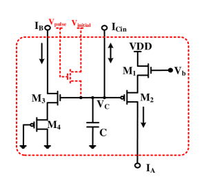
Setting and in (1) and (2) and differentiating with respect to time, the current expression for (see Figure 1) yields:
| (3) |
| (4) |
(3) and (4) are equal, therefore:
| (5) |
where . Similarly, we can derive the following equation for transistors and :
| (6) |
The application of Kirchhoff’s Voltage Law (KVL) and applying the derivative function show the following relations:
| (7) |
| (8) |
where is the capacitor voltage and the bias voltage which is constant (see Figure 1). Substituting (5) and (6) into (7) and (8) respectively yields:
| (9) |
| (10) |
Setting the current in Figure 1 as the state variable of our system and using (3) and the corresponding equation for , the following relation is derived:
| (11) |
Bearing in mind that the capacitor current can be expressed as , relation (12) yields:
| (13) |
One can show that:
| (14) |
Equation (14) is the main core’s relation. In order for a high speed mathematical dynamical system with the following general form to be mapped to (14):
| (15) |
where and are the external and state variable currents, the quantities and must be respectively equal to and . Note that the ratio value can be satisfied with different individual values for and . These values should be chosen appropriately according to practical considerations (see Section V.G). Since is a bilateral function, in general, it will hold:
| (16) |
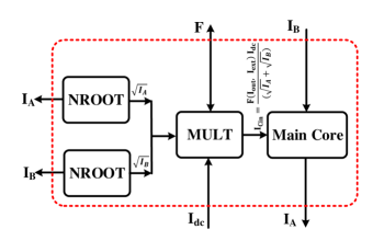
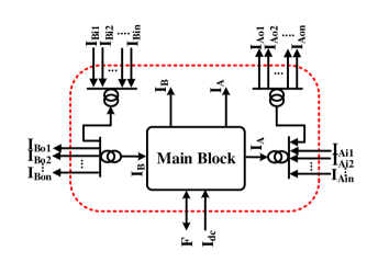
where and are calculated respectively by a root square block (see Figure 2(a) and is separated to + and – signals by means of splitter blocks. Note that is a scaling dc current and has dimensions of . Since can be a complicated nonlinear function in dynamical systems, we need to provide copies of or equivalently of and to simplify the systematic computation at the circuit level. Therefore, the higher hierarchical block shown in Figure 2(b) is defined as the NBDS (Nonlinear Bilateral Dynamical System) circuit [16] (see Figure Figure 2(b)) including the main block and associated current mirrors. The form of (15) is extracted for a 1–D dynamical system and can be extended to dimensions in a straightforward manner as follows:
| (17) |
where and .
3 Basic Electrical Blocks
3.1 Root Square Block
This block performs current mode root square function on single–sided input signals. By setting , considering and as the currents flowing respectively into and and all transistors operate in strong–inversion saturation, the governing TL principle for this block becomes (highlighted with dotted blue arrow):
| (18) |
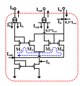
3.2 MULT Core Block
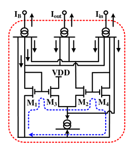
This block is the main core forming the final bilateral multiplier which is introduced in the next subsection. The block contains six transistors as well as two current mirrors. By assuming and as the currents flowing respectively into and and the same aspect ratio for all transistors operating in strong–inversion saturation, the KVL at the highlighted TL with dotted blue arrow yields:
| (23) |
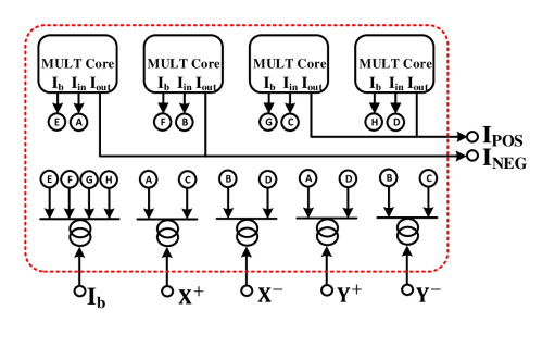
3.3 Bilateral MULT Block
This block is able to perform current mode multiplication operation on bilateral input signals. If inputs are split to positive and negative sides we have:
| (28) |
The multiplication result can be expressed as . By extending equation (27) to for every basic MULT core block, the output signal constructed by a positive and negative side can be written as:
| (29) |
and by further simplifications:
| (30) |
3.4 Circuit Realization of FHN neuron model
The systematic synthesis procedure provides the flexibility and convenience required for the realization of nonlinear dynamical systems by computing their time-dependent dynamical behavior. In this subsection, we showcase the methodology through which we systematically map the mathematical dynamical models onto the proposed electrical circuit. Here, the application of the method is demonstrated by synthesizing the 2–D nonlinear FitzHugh–Nagumo neuron model. In the FHN neuron model [25] with the following representation: and describing the membrane potential’s and the recovery variable’s velocity, the state variables in the absence of input stimulation remain at , while these values go up to in the presence of input stimulation. According to this biological dynamical system, we can start forming the electrical equivalent using (17):
| (31) |
where , , and are functions given by:
| (32) |
where , , and .
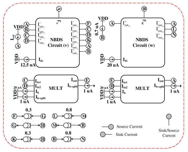
Schematic diagrams for the FHN neuron model is seen in Figure 5, including the symbolic representation of the basic TL blocks introduced in the previous sections. According to these diagrams, it is observed how the mathematical model is mapped onto the proposed electrical circuit. The schematic contains two NBDS circuits implementing the two dynamical variables, followed by two MULT and current mirrors realizing the dynamical functions. As shown in the figure, according to the neuron model, proper bias currents are selected and the correspondence between the biological voltage and electrical current is .

| Specifications | Value |
| Power Supply (Volts) | 3.3 |
| Bias Voltage (Volts) | 3.3 |
| Capacitances (pF) | 800 |
| ratio of PMOS and NMOS Devices () | and |
| Static Power Consumption () | 8.94 |
4 Discussion
Here, we demonstrate the simulation–based results of the high speed circuit realization of the FHN neuron model. The hardware results simulated by the Cadence Design Framework (CDF) using the process parameters of the commercially available AMS 0.35 CMOS technology are validated by means of MATLAB simulations as shown in Figure 6. For the sake of frequency comparison, a regular spiking mode is chosen. Generally, results confirm an acceptable compliance between the MATLAB and Cadence simulations while the hardware model operates at higher speed (almost 1 million times faster than real–time). Table 1 summarizes the specifications of the proposed circuit applied to this case study. As shown in the table, the circuit uses a higher compared to the subthreshold version to force the circuit to operate in strong–inversion region. This comes at the expense of higher power consumption (95000 times higher than the subthreshold version).
References
- [1] S B Furber, F Galluppi, S Temple, and L A Plana. The spinnaker project. Proceedings of the IEEE, 102(5):652–665, 2014.
- [2] H Soleimani and A Ahmadi. A gpu based simulation of multilayer spiking neural networks. In 19th Iranian Conference on Electrical Engineering, pages 1–5. IEEE, 2011.
- [3] Tesla k80 gpu accelerator. Board Specification https://images.nvidia.com/content/pdf/kepler/Tesla-K80-BoardSpec-07317-001-v05.pdf, 2015.
- [4] Intel xeon processor e5–4669 v3. http://ark.intel.com/products/85766/Intel-Xeon-Processor-E5-4669-v3-45M-Cache-210-GHz, 2016.
- [5] J M Nageswaran, N Dutt, J L Krichmar, A Nicolau, and A V Veidenbaum. A configurable simulation environment for the efficient simulation of large-scale spiking neural networks on graphics processors. Neural networks, 22(5):791–800, 2009.
- [6] H Soleimani and M Drakakis, E. A low-‐power digital ic emulating intracellular calcium dynamics. International Journal of Circuit Theory and Applications, 46(11):1929–1939, 2018.
- [7] H Soleimani and M Drakakis, E. An efficient and reconfigurable synchronous neuron model. IEEE Transactions on Circuits and Systems II: Express Briefs, 65(1):91–95, 2017.
- [8] T Matsubara and Torikai. Asynchronous cellular automaton-based neuron: theoretical analysis and on-fpga learning. IEEE transactions on neural networks and learning systems, 24(5):736–748, 2013.
- [9] A Cassidy and A G Andreou. Dynamical digital silicon neurons. IEEE Biomedical Circuits and Systems Conference, pages 289–292, 2008.
- [10] T Hishiki and H Torikai. A novel rotate-and-fire digital spiking neuron and its neuron-like bifurcations and responses. Neural Networks and Learning Systems, IEEE Transactions on, 22(5):752–767, 2011.
- [11] H Soleimani, A Ahmadi, and M Bavandpour. Biologically inspired spiking neurons: Piecewise linear models and digital implementation. Circuit and System I Regular Paper, IEEE Transactions on, 59(12):2991–3004, 2012.
- [12] H Soleimani, M Bavandpour, A Ahmadi, and D Abbott. Digital implementation of a biological astrocyte model and its application. IEEE Trans. Neural Netw. Learn. Syst., 26(1):127–139, 2015.
- [13] H Soleimani and E M Drakakis. A compact synchronous cellular model of nonlinear calcium dynamics: simulation and fpga synthesis results. IEEE Trans. Biomedical Circuit and Systems, 17(3):703–713, 2017.
- [14] E Jokar and H Soleimani. Digital multiplierless realization of a calcium-based plasticity model. IEEE Transactions on Circuits and Systems II: Express Briefs, 64(7):832–836, 2016.
- [15] A Makhlooghpour, H Soleimani, A Ahmadi, M Zwolinski, and M Saif. High accuracy implementation of adaptive exponential integrated and fire neuron model. In 2016 International Joint Conference on Neural Networks (IJCNN), pages 192–197. IEEE, 2016.
- [16] E Jokar, H Soleimani, and M Drakakis, E. Systematic computation of nonlinear bilateral dynamical systems with a novel low-power log-domain circuit. IEEE Transactions on Circuits and Systems I: Regular Papers, 64(8):2013 – 2025, 2017.
- [17] S S Woo, J Kim, and R Sarpeshkar. A cytomorphic chip for quantitative modeling of fundamental bio-molecular circuits. Biomedical Circuits and Systems, IEEE Transactions on, 9(4):527–542, 2015.
- [18] G Indiveri, E Chicca, and R Douglas. A vlsi array of low-power spiking neurons and bistable synapses with spike-timing dependent plasticity. Neural Networks, IEEE Transactions on, 17(1):211–221, 2006.
- [19] A Houssein, K I Papadimitriou, and E M Drakakis. A 1.26 w cytomimetic ic emulating complex nonlinear mammalian cell cycle dynamics: Synthesis, simulation and proof-of-concept measured results. Biomedical Circuits and Systems, IEEE Transactions on, 9(4):543–554, 2015.
- [20] K I Papadimitriou, G B V Stan, and E M Drakakis. Systematic computation of nonlinear cellular and molecular dynamics with low-power cytomimetic circuits: a simulation study. PloS one, 8(2):e53591, 2013.
- [21] S Moradi and G Indiveri. An event-based neural network architecture with an asynchronous programmable synaptic memory. Biomedical Circuits and Systems, IEEE Transactions on, 8(1):98–107, 2014.
- [22] M Bavandpour, H Soleimani, S Bagheri-Shouraki, A Ahmadi, D Abbott, and L O Chua. Cellular memristive dynamical systems (cmds). International Journal of Bifurcation and Chaos, 24(5):1430016–1–1430016–22, 2014.
- [23] M Bavandpour, H Soleimani, B Linares-Barranco, D Abbott, and L O Chua. Generalized reconfigurable memristive dynamical system (mds) for neuromorphic applications. Frontiers in neuroscience, 9(409):1–19, 2015.
- [24] H Soleimani, A Ahmadi, M Bavandpour, and O Sharifipoor. A generalized analog implementation of piecewise linear neuron models using ccii building blocks. INeural networks, 51:26–38, 2014.
- [25] R FitzHugh. Impulses and physiological states in theoretical models of nerve membrane. J. Biophys., 1(6):445–466, 1961.