Linear Delay-cell Design for Low-energy Delay Multiplication and Accumulation
Abstract
A practical deep neural network’s (DNN) evaluation involves thousands of multiply-and-accumulate (MAC) operations. To extend DNN’s superior inference capabilities to energy constrained devices, architectures and circuits that minimize energy-per-MAC must be developed. In this respect, analog delay-based MAC is advantageous due to reasons both extrinsic and intrinsic to the MAC implementation (1) lower fixed-point precision requirement for a DNN’s evaluation, (2) better dynamic range than charge-based accumulation, for smaller technology nodes, and (3) simpler analog-digital interfacing. Implementing DNNs using delay-based MAC requires mixed-signal delay multipliers that accept digitally stored weights and analog voltages as arguments. To this end, a novel, linearly tune-able delay-cell is proposed, wherein, the delay is realized using an inverted MOS capacitor’s () steady discharge from a linearly input-voltage dependent initial charge. The cell is analytically modeled, constraints for its functional validity are determined, and jitter-models are developed. Multiple cells with scaled delays, corresponding to each bit of the digital argument, must be cascaded to form the multiplier. To realize such bit-wise delay-scaling of the cells, a biasing circuit is proposed that generates sub-threshold gate-voltages to scale ’s discharging rate, and thus area-expensive transistor width-scaling is avoided. For 130nm CMOS technology, the theoretical constraints and limits on jitter are used to find the optimal design-point and quantify the jitter versus bits-per-multiplier trade-off. Schematic-level simulations show a worst-case energy-consumption close to the state-of-art, and thus, feasibility of the cell.
Index Terms:
Analog-computing, delay-cell, mixed-signal delay multiplier, multiply-and-accumulateI Introduction
Recent advances in machine learning algorithms and, particularly, deep neural networks (DNNs), have equipped portable computing devices with human-like inferring, classifying and planning capabilities. Enormous sizes of these networks, with number of operations per evaluation often running into millions, make remote computing servers indispensable. Reliance on servers increases inference latency, communication energy, risk of privacy loss, traffic, and needs a perpetual connection to the server. Some of these metrics are critical in applications like self-driven cars, that cannot afford delays while making decisions. Delocalizing computational effort for evaluating ML model, away from server and towards the leaf nodes, requires ML-specific energy-efficient computing architectures [1]. Many such architectures have been proposed to greatly accelerate the training and inference speed of DNNs [2, 3, 4], but much work is needed to efficiently run these networks under severe energy restrictions many portable devices operate under.
The computing-energy’s problem [5] is tackled by: (1) using simpler data-types: these algorithms do not require a large precision and continue to provide similar accuracy with simpler data-types and restricted widths [6, 7, 8, 9, 10, 11] (2) minimizing data-transfer: the number of data-fetches shoots up for human-level, large-scale applications of these algorithms causing significant non-compute (latent) energy losses [2, 4, 12].
Relative robustness of DNNs to precision-loss, together with a limitation on energy, motivates the use of analog computing systems, wherein, the loss of information due to noise and process-variability can effectively be modeled as the loss in precision. To maintain the energy-efficiency without an excessive (counter-productive) precision-loss, these systems constitute both analog and digital computing units. The computational roles are distributed such that the multiply-and-accumulate (MAC) operations, which form the bulk of a DNN’s evaluation, are executed in an analog domain, while other operations (e.g. control-flow, data-communication and storage) are done using binary voltages. Superposable electrical variables like charge [13, 14] and current [15, 16, 17] physically represent partial sums of a MAC, with a capacitor as a an accumulator to store the sum of physical variables.
Recently, time was proposed as an accumulation variable, as it is better than charge and current in following regards: (1) time-to-voltage/digital converters (TDC, and vice versa – DTC) are more area and power-efficient than voltage-based converters [18, 19]. For instance, both DTC and TDC can be realized out of clocked counters, while voltage ADC/DACs require area and energy-expensive operational amplifiers; (2) while the noise-floor is relatively constant, the supply voltage, , drops with technology nodes. Thus, the dynamic-range of accumulation of voltage, current or charge gets increasingly limited; (3) the transition frequency of the FETs, which dictates the temporal resolution of a TDC, increases with tech. nodes.
Within the purview of time-based accumulation, pulse-width [20, 21] and pulse-delay [18, 22, 23] are the two modulation schemes that have been demonstrated on-chip. Of these, pulse- (or, event) delay is more promising for MAC applications due to (1) free addition/subtraction in case of delay, and (2) requirement of peripheral pulse re-routing circuitry requirements in the prior.
A practical delay-MAC must meet following specifications: firstly, it must accept mixed-signal arguments one analog while other digital, for locally stored weights; secondly, it should posses linear voltage-delay (transfer) characteristics to accept externally sensed analog voltages and allow cascading of multiple layers of MACs. To implement a low-energy mixed-signal delay-multiplier, major challenge is the design of a tune-able delay-cell, having linear transfer characteristics. Miyashita et al. [18] first proposed the use of analog-digital mixed signal delay-MAC. Common mathematical operations like addition, subtraction, multiplication, and max-/minimization were demonstrated in a clocked time-domain. However, the multiplication using clocked time-to-digital converters negated power-savings expected from an analog processor. Clock-less tune-able delay-cells for MACs were later proposed in [22], where the accumulation after each dot-product in a binary convolutional neural network was carried implicitly by the delays of a series of nMOS resistor-based delay-cells. However, the use of resistors for enabling scaling of delay, lead to an area-expensive solution.
Delay-modulation via programming voltages, for both low-power front-end analog processing and approximate-computing acceleration, was demonstrated in [23]. Applying a small-signal analog input to the back-gate of the transistor modulated the threshold voltage and hence, the delay. Since the threshold voltage varies with the input in a square-root fashion, the delay is inherently non-linear. Also, variation in the threshold voltage across a chip can introduce non-homogeneity in the multiplier.
In this work, a novel CMOS referential delay-cell, based on a steady discharge of a MOSCAP () via a constant current (), is proposed. Block-diagram in Fig. 1 depicts three sequential processes that undergoes, from :
-
1.
instantaneous pre-charge to (colored red)
-
2.
steady discharge, through a constant current (blue)
-
3.
thresholding of at , using a threshold detector (green).
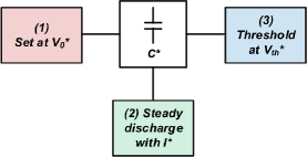
With these three processes, time taken for to reach is:
| (1) |
If is a linear function of , then time taken to discharge to (or simply, the delay) becomes a linear function of . This forms the basis of the proposed delay-cell. For use within a multiplier, its delay is exponentially scaled through gate-voltages of the source of , rather than transistor widths. Next, analytical models for all the sub-processes in the delay-cell are developed, key sources of jitter identified and a model for the net jitter is formed. From these models, constraints on and for the usability of delay-cells in a multiplier are found, and it’s shown that the multiplier cannot accommodate more than 5 bits of (signed) digital-input. Biasing circuits that generate the gate-voltages to scale and the delay exponentially, are then proposed and validated.
The paper is divided as follows: in Sec. II, necessary but brief background on mixed-signal delay multipliers, delay-MACs and how multiple delay-cells together constitute a multiplier, is presented. In Sec. III, the concept behind the proposed delay cell is presented in more details. For each of the three sub-processes, CMOS implementation details are presented and constraints for a linear delay transfer characteristics developed. Jitter-models are then developed for the two sub-processes that contribute most to the jitter. In Sec. IV, the constraints and jitter model developed are employed to find the minimum latency and maximum number of bits that can be accommodated within the multiplier. Also, a biasing circuit that enables an accurate exponential scaling of delays of cells within a multiplier is presented. In Sec. V, we discuss about the chosen noise-floor and its connection with the maximum number of bits, and input dependence of energy consumption. Next, the proposed delay-cell is compared with the state-of-art, before concluding in Sec. VI.
II Background
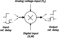


A delay-MAC comprises of several delay multipliers, whose delays serially accumulate, before undergoing further non-linear processing. The multiplier accepts a time-referenced event signal, which it propagates forward as-is, but after a delay in proportion to the product of its arguments. When several such multipliers are placed in series, and a reference event is applied to the first, then, the ref. event is propagated forward, and the net (accumulation of) delay models the dot-product of inputs. By using delays, the need of adders is eliminated, because the delays are summed up naturally. Since negative numbers cannot be represented using individual events, a pair of events is used, where, the time of instance of one’s occurrence referred to the other’s, is called referential delay (Fig. 2).
A delay multiplier, besides two input arguments, has a pair of a variable and a reference event-signals (henceforth called referential events) at its input and output. For a mixed-signal multiplier, a signed, fixed-point weight vector ( and an n-bit wide vector ) and an analog scalar () form the argument, and a pair of rising (or, falling) edges of voltages form referential event-signals (Fig. 2). To accommodate negative weights, symmetric 2:2 multiplexers (or, relays) are placed within each multiplier that are realized using transmission-gates. The relay ensures that for each negative weight, the referential events are swapped before multiplication (Fig. 3a,b).
Each multiplier consists of smaller referential delay-cells that correspond to each bit of and create a referential delay equaling , where, is the common delay-factor and . The common delay-factor, , is a linear function of . For reasons explained Sec. III-C, two, falling edges, as referential event signals, are propagated through the multiplier. Weight bits, , individually determine whether reference-event signals are delayed by or not, by making the falling-edge pass or skip a delay-cell.
Each referential delay-cell has a pair of identical and parallel, linearly tunable delay-cells. One delay-cell inputs and outputs the falling-edge after delay linearly dependent on . The second cell inputs a constant reference voltage, , and outputs the event after a fixed time. If , then variable event gets more delayed compared to the reference, which represents a positive partial sum. A negative partial sum is produced if and zero, if . Thus, using a pair of delay-cells homogenises the multiplier with respect to the multiplicand and allows negative weights and referential delays.
For illustration, a 1-bit multiplier is shown in Fig. 3a. The multiplier comprises of a 2:2 relay and a referential delay cell. implies a negative weight which causes the falling-edges to get swapped. The referential delay-cell further contains two delay-cells, with one variable input () and the other with a reference input (). When , cell-bypassing MUX is enabled leading to both negligible delay and ref. delay. Next, 3-bit multiplier is shown in Fig. 3b. The referential delays are scaled in the ratio 1,2 and 4, by scaling the absolute delays in the ratio 1,2 and 4.
One may also use differential mode of operations, where, the referential-delay cell is replaced with differential delay-cell. In this mode, the analog input are changed from and to and . This may remove second order distortion terms of the multiplier without changing the multiplier’s circuitry.
III Delay-cell Design in CMOS
III-A Steady discharge-based delay-cells
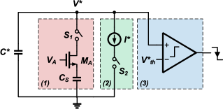


An idealized circuit implementing this process’s equivalent is shown in Fig. 4, where, each component responsible for the three sub-processes have been boxed and colored correspondingly.
In branch 1, the key component is a -accepting that has a net source-capacitance . Initially, both and are open and is charged to . Once is closed, NFET initializes by sinking its charge into , until its source-voltage reaches approximately below the gate voltage, to . From charge conservation, the lowers by:
| (2) |
Thus, the n-FET conducts until the source voltage rises enough to cut-off the channel, establishing a linear relationship between and . The approximation in Eq. 2 comes from the fact that a real sub-micron FET doesn’t have a well defined threshold-voltage. However, as later shown in Sec. III-C, the linear relationship still holds well if .
Once the voltage across is set, is opened and is closed causing to spontaneously discharge via , at a constant rate (Fig. 4). The steady discharge process can be described as:
| (3) |
where, is the drop in below . Next, a threshold-detector, with a threshold , outputs a falling-edge once drops below . Time taken for () to reach a given threshold , called the absolute delay (), is given by:
| (4) |
This is a linear function of . So, the delay can be adjusted linearly with the input (Fig. 5). As discussed in II, to homogenize the delay-input relationship, referential delay is used. For a pair of steady discharge based delay-cells, the referential delay is:
| (5) |
which, is independent of . In case varies with , the referential delay may be written as:
| (6) |
For to be a linear function of , needs to be maximally constant for the range of . If is scaled (exponentially) by factor of (Fig. 5), then a delay multiplier with a digital input vector will yield the following referential delay:
| (7) |
where, is the ref. delay from the delay cell i. This forms the basis of our mixed-signal delay multiplier.
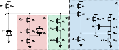
The schematic of the delay-cell in CMOS is given in Fig. 6, detailed design methodology of which, is discussed next.
III-B CMOS implementation:
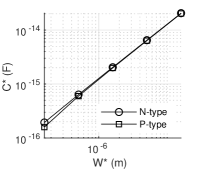
Later in Sec. IV-A, it is shown that of approximately is optimal for minimizing energy, latency and jitter. An inverted MOSCAP, steadily discharging towards depletion, reliably provides capacitance in this range. Since an n-type MOSCAP has a larger inversion capacitance-density than p-type (Fig. 7), the prior is used.
III-C CMOS implementation: Voltage initialization
This stage comprises of min. sized transistors and pMOSCAP in Fig. 6, key design considerations of which are discussed next:
-
1.
Input nFET (): To nullify effect of process variations (PV), the -accepting nFET is unique to a multiplier, i.e. it is shared by all delay-cells within a multiplier. Specifically, random dopant-fluctuation, oxide-thickness variations and other process-related non-idealities may offset , that may in-turn offset output ref. delay by:
(8) where, models effect of PV
-
2.
: This capacitor is unique to a delay-cell, and a min. sized pFET is assigned to each cell. The pFET stays in the inversion regime regardless of , because saturates to a value that is at least less than
-
3.
Switch S-1 (): In the relevant regime of operation, remains close to , necessitating a p-type FET. The switch is unique to each delay-cell, as it isolates of each cell from a shared of the multiplier
-
4.
Reset switch (): A switch to reset the to zero before each computation is kept common to all cells within a multiplier
If the initial charge on is zero, then, can be expressed as a linear function of and an offset term:
| (9) |
Here, is the parasitic capacitors, arising from and ; models the zero-offset at dependent on several parameters: , ’s width and other parasitic effects like feed-forward of input falling-edge into . Note that has two distinct values: first is defined within the discharge-pulse application (MD) and it contains a feed-forward component of the falling-edge. The second is defined after the discharge-pulse application (PD), and is slightly less than MD.
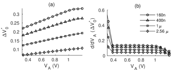
To quantify linearity, is plotted in Fig. 8 against and its derivative w.r.t. in 8b for ranging between and , with (or ) as parameters of design. For this range, less than 10% variation is seen. The figure shows that larger capacitors can provide better linearity.
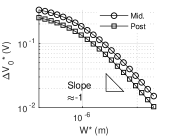
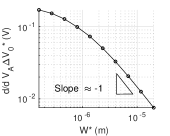
Fig. 9 plots the for and its average derivative, versus (), in a log-log fashion. Both plots have a constant slope of for sufficiently large , validating Eq. 9 as a model for the discharge process. and are then empirically determined by fitting the model of Eq. 9, yielding and (MD).
Eq. 9 is only valid when the ’s voltage is big enough to charge up . Mathematically,
| (10) |
For , we get:
| (11) |
This sets the lower limit on , which is employed later in Sec. IV-A.
To slightly enhance the linearity without adding to the area, one in every 5 pMOSCAP of the is replaced by an nMOSCAP. For , PFET is inverted and provides a close to a constant cap. For , pFET’s capacitance diminishes but nFET offsets the loss. Since NMOS is smaller, it does so, only to a small extent.
III-D CMOS implementation: Steady discharge
This part of the delay-cell consists of transistors in Fig. 6, key design considerations of which are discussed next:
-
1.
: This is realized using bi-cascoded nFET current source, with the FETs at their min. widths. The exponential current scaling is done via an external biasing circuit, that generates gate-voltages for both and . The biasing circuits are discussed in Sec. IV-B.
-
2.
Switch S-2 (): An NMOS switch is placed in series with the current-source. Unlike S-1, the switch was placed away from , preventing the feed-forward through the parasitic capacitors.
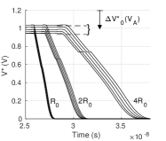
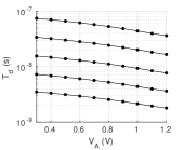
For () at its minimum value () and , ’s discharge transient is shown in Fig. 10a. Referring back to Fig. 6, the switch () is turned ON at , by ramping-up , the input to . As expected, discharges at a near-constant rate (Fig. 10a). Its constancy depends solely on output resistance of the current source. Kinks observable in the transients are caused by the feedback from the half-latch and do not practically affect the performance. The absolute delay for various (), spaced exponentially with a factor of 2, is plotted in Fig. 10b.
III-E CMOS Implementation: Threshold detector
It comprises of as the falling-edge, uni-polar threshold detectors, half-latch and other switches for resetting. Details and design consideration are discussed next:
-
1.
Falling-edge inverter (): To minimize the area requirements, the width of is kept minimum. As discussed below, under certain constraints on , this inverter contributes to a -independent delay, thus keeping distortion negligible
-
2.
Leak-prevention switch (): It prevents the sub-threshold from leaking and set-up the latch pre-maturely. It inputs the falling-edge of the previous delay cell
-
3.
Half-latching inverter (): These transistors latch to and the -node to , once reaches
-
4.
Latch-en-/disable switches (): These switches enable the half-latch operation when closed and otherwise, disable it, reducing the energy required to reset the half-latch
-
5.
Reset-FETs (): resets node to 0. sets the OFE node to before the start of computation. These transistors are shared within the multiplier
A CMOS inverter can serve as a low-energy threshold detector, whose switching-voltage can be set by designing the ratio of sizes of pMOS and nMOS. However, it consumes short-circuit energy () given by:
| (12) |
where and,
Since decreases exponentially, increases exponentially. Hence, a delay-cell implementing the n-th exponent will expend the of the cell implementing the first. For a n-bit multiplier, the total short-circuit energy lost is . Thus, an exponential requirement in energy consumption motivates an alternative inverting mechanism.
The low-energy alternative to the CMOS inverter is a standalone pFET ( in Fig. 6), due to its switch-like I-V relationship. If it were an ideal switch, with a switching voltage ), would jump to after a fixed delay following . This would conserve the linearity of Eq. 5 with respect to , as it only adds a constant delay. However, a real PFET has a close to exponential I-V relationship and conservation of linearity needs to be established, or at least constraints for maximal linearity determined.
With the assumption of exponential I-V characteristics and large output-resistance (), the sub-threshold current can be expressed as a function of the gate-source voltage () using the following equation:
| (13) |
where, is the thermal voltage. Eq. 13 is valid only for ; for , I-V relationship is usually degree-2 or less polynomial, moving the switch away from an ideal behavior.
For a that linearly decreases from with a steady rate , (Fig. 6) can be expresses as a function of time using:
| (14) |
where, is the rate of change of with time, and is net capacitance at the drain of M8. When , the half-latch is set up and the voltage at node (Fig. 6) falls to . Thus, the time taken from the start of discharge () to the drop in -node voltage to zero is:
| (15) |
becomes a linear function of under the constraint:
| (16) |
Putting , this inequality may alternatively be written as:
| (17) |
Since varies inversely with (from Eq. 9), the denominator in Eq. 17 is a monotonically decreasing function of . Then, as per this inequality, should be greater than a critical capacitance . This inequality is used in Sec. IV-A, for establishing constraints on and .
Under the validity of this inequality, can be expressed as:
| (18) |
matching the expectation of ’s linearity with , or . Note that the latch-point, or, the value of when is a constant, independent of (or ), and expressible as:
| (19) |
Though an exponential I-V characteristics is assumed for , in reality, it is exponential only for sub-threshold gate voltages. For devices with power I-V relations, Eq. 14 is re-derived with the modified I-V, and constraints of Eq. 11 re-determined. For power current-voltage relationship,
| (20) |
For an ideal switch (), the constraint is trivially satisfied and TD stage doesn’t contribute to distortion. As the I-V relationship of the pFET moves away from step-like behaviour towards linearity (), ensuring linearity from delay- characteristics becomes harder.
III-F Noise-modelling
The delay-cell essentially consists of two current-integrators that accumulate the accompanying noise-current, starting from the arrival of falling-edge () to the latch-up (). This leads to a net temporal shift in the falling-edge, or a jitter in the output falling-edge. To enable design of the delay-cell and multiplier, the two jitter components are modeled as a function and (the design variables) and an upper limit on jitter is set, yielding constraints on the design variables and . For simplifying jitter-modeling, it is assumed that:
-
1.
Out of the three, only two processes contribute to the jitter: steady discharge and threshold-detection. (Initial discharge occurs much faster than , so it contributes negligibly to the net jitter.)
-
2.
The net jitter is much smaller than
III-F1 Jitter from steady discharge
For this stage, the primary contributor of jitter the is channel noise-current from accumulating in . To simplify the model, it is assumed that the noise-current out of circulates within itself, and hence contributes negligibly to the jitter. With this assumption, the stage reduces to a noisy FET discharging a fixed capacitor, jitter modelling for which was done for ring oscillators in [24]. For an inverter-type ring-oscillator, the jitter-per-stage is modeled as:
| (21) |
where, is the excess noise factor, is the drain-source conductance at . This naturally extends to the proposed delay-cell, with the exception that is variable, dependent on the rate of discharge and . Using Eq. 4 the expression for jitter becomes:
| (22) |
To further simply, the dependence of jitter on and is neglected and a constant jitter, for a drop in , is defined and used. Owing to the fact that has a linear dependence on current, jitter from this stage is compactly express-able as:
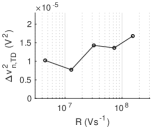
| (23) |
where, is a temperature and technology dependent constant. For model validation, the jitter is simulated in software, for IBM’s technology. Resulting , with only noise turned on, versus and is plotted in Fig.11.
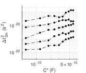
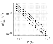
Instead of Eq. 23, the following model is used as it fits the experimental data better (R-sq. of 0.982, from 10 iterations):
| (24) |
where, and .
III-F2 Jitter from threshold detector
Since the input gate-source voltage () of increases linearly with time and drain-current exponentially, it is assumed that RMS channel noise-current out of increases exponentially. Thus, at any given instant of time post falling-edge’s arrival, noise current from only the past 3-4 -drops in , contributes to this stage’s jitter.
If is the deviation in at , then for a constant , we have:
| (25) |
Since varies exponentially over the duration , this equation cannot be applied without adjustments. Thus, the following equation is used:
| (26) |
Letting , we get:
| (27) |
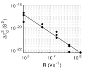
where, . This equation establishes an independence of on , which is confirmed from Fig. 12. In the figure, is varied by a factor of more than , but less than rise is seen in .
Next, the relationship between and is determined. Similar to the approach adopted in [24], can be found by extrapolating noisy along the noise-less , to the point of latch-up:
| (28) |
where, Eq. 14 was used for . Simulated jitter, with only ’s noise turned on, is plotted in Fig. 12.
For minimally sized , the fitted model from 10 iterations of (noisy) simulations is:
| (29) |
where, . Thus, the actual exponent is less than predicted.
IV Mixed-signal Delay Multiplier
With the delay-cell design considerations discussed, next, the necessary steps to employ the cells within a multiplier are presented: (1) use of constraints to find the valid region of design and operation (2) bias-circuit design for ’s exponentiation. Lastly, through simulations, the functionality of cascaded delay-cells as multiplier is validated and the key energy components for each multiplication operation are identified.
IV-A Optimizing and No. of Bits
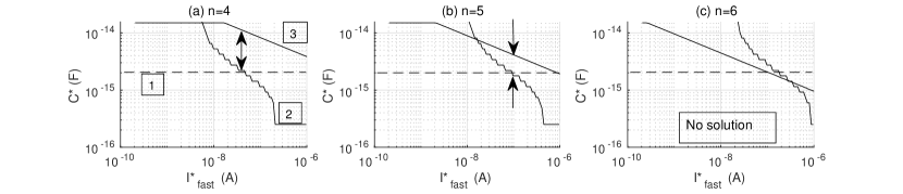
Using the inequalities involving , developed in Sec. III-C, Sec. III-E and the noise models of Sec. III-F, the constraints on and are determined. Note that these are valid only for the IBM’s technology, but may similarly be determined for other CMOS technology nodes.
IV-A1 Linearity of voltage-initialization
In the inequality of Eq. 11, replacing model-parameters extracted from the data of Fig. 8-9 gives constraint 1,
| (30) |
which, corresponds to an inverted nMOSCAP single-finger width of . This constraint is marked by ’1’ in Fig. 13a-c.
IV-A2 Linearity of threshold detection
Since of the slowest cell is times smaller than than that of the fastest cell (), constraint 2 from Eq. 17 becomes:
| (31) |
IV-A3 Upper limit on jitter
The referential delay of the fastest cell, from Eq. 5, is:
If jitter from steady discharge is denoted by and from TD by , the constraint on the net jitter is such that it is to be smaller than the maximum ref. delay of the fastest cell. For a ,
| (32a) | |||
| (32b) | |||
With its LHS being monotonic function of , Eq. 32 gives an upper limit on for a given . This constraint is marked by ’3’ in Fig. 13a-c.
Fig. 13 plots the constraints for a 4, 5 and 6-bit multiplier. For 4 and 5 bits, the valid region of operation, marked by double-sided arrows, lies between the curves corresponding to constraints 1, 2, and 3. For 6 bits, no solution exists for the chosen constraints. Thus, the 5-bit multiplier with
and
emerges as the point of design, as it works for all multipliers with less than 6 bits, minimizes the multiplication latency and energy consumption.
IV-B Biasing circuit
Accurate biasing for the current sources is required to ensure low output distortion. As discussed below, its behavior must meet two specifications:
-
1.
As discussed in Sec. IV-A, is achievable only for the sub-threshold transistors with the employed VLSI node. Hence, the biasing circuit is designed only for sub-threshold currents and works well in this regime only
-
2.
The current source within each cell consists of a pair of series NFETs ( and in Fig. 6). ’s gate-voltage (primary bias) is such that it sinks and its drain-voltage is fixed close to (). The drain voltage is maintained by gated with a secondary bias approximately above
The circuit (Fig. 14) has two branches: source and scaling. Source branch () generates biasing voltages dependent on a programmable voltage, . Scaling branch () first uses those biasing voltages to generate current in the exponents of 2 (using transistor widths) and then generates the bias for the cells’ current-source using self-biasing. Here, the primary bias out of is denoted as and the secondary out of as .
In the source branch, converts the reference voltage into current . and , being self-biased in the saturation regime, push up the gate voltages of the tri-cascode, enough to keep mirror transistors () of the scaling branch saturated. produce the multiplier-cascode’s bias.
In the scaling branch, ’s widths are down-scaled by w.r.t. the source cascode’s width, which down-scale the current in the same proportion. is self-biased to accept the current and generates the primary bias . The gate voltage of the FET with the largest current exponent (or, the smallest delay exponent) is:
| (33) |
Its drain-voltage is maintained at using a fixed biased . After down-scaling ’s size (by , being the exponent), its source voltage is maintained at a constant value. , also a down-scaled transistor, is used to generate the secondary bias (). ’s width is adjusted using parametric analysis to keep its self-bias above by . An additional exponent-dependent scaling for the is needed, given by:
| (34) |
to counter the lower turn-on voltages is required for the scaling branches. The response of the bias circuit is plotted in Fig. 15. As varies, the bias current input to the multiplier’s cascode is plotted in Fig. 15. , and of down-scaled multiplier branches (upto 8 bits) is plotted in Fig. 15.
To minimize distortion, it is essential that ’s corresponding to all exponents are applied the same drains-source voltage. Besides using a 3-level cascoding, the length of all transistors within the cascode is increased by over the minimum to minimize the CLM and short-channel effects that shoot-down the . The sizes of all transistors are summarized in Table I.


| FET Label | Width () | Length () |
|---|---|---|
| 10 | ||
| 1 | 1 |
IV-C Multiplier Simulation
Using the peripheral elements described in Sec. II, the multiplier is simulated using transient simulators, for IBM technology.
IV-C1 Functionality test
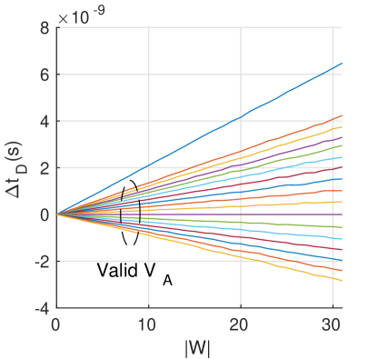
A 5-bit multiplier, composed of delay-cells cascaded as described in Sec. II, was simulated. Letting , Fig. 16a plots the ref. delay of the multiplier as it varies with , with weight () as a parameter. Conversely, ref. delay with as the independent variable and as parameter is plotted in Fig. 16b. Since the output ref. delay is distorted for , the valid range of inputs for the multiplier is to .

IV-C2 Energy analysis and simulation results
Within a delay cell, the key components of energy are:
-
1.
: Energy used up in charging for each computation. It is given by:
(35) The actual value may vary due to parasitic capacitance and the dependence of on
-
2.
: Energy stored in node corresponding to (6), once crosses the threshold. It is given by:
(36) where, is the net capacitance at the node. Part of it comes from the thresholding-pFET () and other comes from latching-pFET, ()
-
3.
: Energy used in pull-up of the event-propagating wires of the delay cell ( node in Fig. 6)
-
4.
: Energy used up in inverting the input falling-edge, to a rising edge (, input to in Fig. 6)
Next, value of these metrics is determined by simulating the 5-bit multiplier (schematic) for one cycle of computation, with arguments and . , and is determined during the computation-phase and and are determined during pre-charge phase. The energy components and their simulated values are listed in Table II. Comparing their sum with the simulated total, it is concluded that the listed components account for almost all the expended energy.
| Component | Energy/MAC (fJ) | Energy/MAC/bit (fJ) |
|---|---|---|
| 34.0 | 6.8 | |
| 5.6 | 1.1 | |
| 8.8 | 1.7 | |
| 46.0 | 9.0 | |
| 16.0 | 3.0 | |
| Total | 110 | 22 |
| Total (sim.) | 116 | 23 |
V Discussion and Bench-marking
In Sec. IV-A3, constraint on jitter was chosen such that the peak-jitter () from the slowest delay-cell, is less than the maximum referential delay of the fastest delay-cell. However, for certain inputs, the net output referential delay of a multiplier can be zero, which makes it impossible for for the noise to ever be smaller than the output signal. Thus, the chosen constraint is a practical as it grants the benefit of lower energy consumption by delay-based analog computing and simultaneously prevents excessive signal corruption by the noise. Depending on the signal-to-noise specification for an application, much tighter constraint on noise may be placed, which, in effect, reduces the maximum number of bits accomodable. Fig. 17 plots the number of bits possible within a multiplier, as a function of excess jitter margin (), where, is the ratio of maximum ref. delay of the fastest cell and peak-jitter. At , the number of bits is the highest, and decreases to 1 at .
| This work | Gopal et al. [23] | Miyashita et al. [18] | Sayal et al. [20] | Lee et al. [14] | Skrzyniarz et al. [16] | |
| Domain | Time: delay | Time: delay | Time: Clocked-delay | Time: Pulse-width | Analog-charge | Analog-current |
| Demo. node | 130nm | 65nm | 65nm | 40nm | 40nm | 65nm |
| Input-width | Analog-5b | Analog-3b | 1b | 8b | Analog-3b | 2b/1b |
| Energy (fJ/MAC/bit) | 23 | 7 | 20 | - | 15 | 13 |
| Latency | 1b: 1.2ns and 5b: 50ns | 250ps | 50ps | - | - | - |
| Negative weights | Yes | No | Yes | Yes | No | No |
| Linearity mechanism | Discharge-till-pinch-off | Body-gate biasing | Binary | Binary | NA | NA |
Note that the multiplier’s , given in Table II, is computed for the case when all weight bits are set to 1 (W=31). Otherwise, this components of energy depends on (1) the input weight and (2) number of computations being done by the MAC, per second. If the multiplier is used in a sense, or, one-time-use mode, then, the listed is accurate, as all the charged-up energy leaks out eventually. Any new MAC cycle would require the same energy to charge-up from the point of no charge. However, for acceleration mode, where same weights are used with variable , of the cells with never get an opportunity to discharge completely, since all falling-edges bypass the cell. Before it fully discharges, a new MAC cycle’s pre-charge step would charge-up to from intermediate voltage.
In Table III, two simulated performance metrics are compared with the state-of-art: (1) energy consumption per multiply-accumulate, reported above, and (2) multiplication latency (from absolute delay of the delay-cell). We also compare whether the multiplier allows negative weights and the maximum number bits accommodable for various mixed-signal MACs. From the table, it is seen that:
-
1.
The delay cell consumes per bit of digital argument/input, which, is more than lowest-reported state-of-art energy consumption. Our energy metric is at , and the lowest state-of-art metric at . Assuming that the energy scales by , the scaled energy consumption approaches that of the state-of-art
-
2.
In [23], linearity of the delay-cell is based on back-body biasing, which, is theoretically non-linear. In the proposed cell, the output-input characteristics are linear, due to the linear voltage-initialization step
-
3.
Despite noise limitations, the number of bits that can be accommodated in the mixed-signal multiplier is higher than state-of-art. All reported mixed-signal MACs use an exponential scaling of transistor widths, as a way to convert digital signals to analog. In this work, we proposed a biasing circuit that exponentially scales the currents via gate-voltages and avoid area expensive width-scaling
VI Conclusion
In this work, a linearly tunable delay-cell is proposed that realizes the analog input-dependent delay using three sequential sub-processes: (1) an input-dependant charge-up of (2) its steady discharge, via current (3) thresholding of its voltage. Each of the sub-processes is then analytically modeled, using which, constraints on the and for linearity are found. Jitter models, based on prior ones developed for CMOS inverter ring-oscillator, were modified and validated for the proposed cell. To form a multiplier, delay-cells with same analog input and scaled in the exponents of 2, must be cascaded to form a multiplier. Since is scaled using gates-source voltages, a biasing circuit that accept a ref. voltage and generates gate biases for delay cells corresponding to all exponents, is proposed and validated. From the constraints on for linearity and noise, the minimum was found to be around and maximum bits supportable to be five. Lastly we also identify key energy components of the multiplier, which sum up to be 20 fJ/MAC/bit for IBM’s 130nm technology.
References
- [1] X. Xu, Y. Ding, S. X. Hu, M. Niemier, J. Cong, Y. Hu, and Y. Shi, “Scaling for edge inference of deep neural networks,” Nature Electronics, vol. 1, no. 4, pp. 216–222, 2018.
- [2] N. P. Jouppi, C. Young, N. Patil, D. Patterson, G. Agrawal, R. Bajwa, S. Bates, S. Bhatia, N. Boden, A. Borchers, R. Boyle, P.-l. Cantin, C. Chao, C. Clark, J. Coriell, M. Daley, M. Dau, J. Dean, B. Gelb, T. V. Ghaemmaghami, R. Gottipati, W. Gulland, R. Hagmann, C. R. Ho, D. Hogberg, J. Hu, R. Hundt, D. Hurt, J. Ibarz, A. Jaffey, A. Jaworski, A. Kaplan, H. Khaitan, D. Killebrew, A. Koch, N. Kumar, S. Lacy, J. Laudon, J. Law, D. Le, C. Leary, Z. Liu, K. Lucke, A. Lundin, G. MacKean, A. Maggiore, M. Mahony, K. Miller, R. Nagarajan, R. Narayanaswami, R. Ni, K. Nix, T. Norrie, M. Omernick, N. Penukonda, A. Phelps, J. Ross, M. Ross, A. Salek, E. Samadiani, C. Severn, G. Sizikov, M. Snelham, J. Souter, D. Steinberg, A. Swing, M. Tan, G. Thorson, B. Tian, H. Toma, E. Tuttle, V. Vasudevan, R. Walter, W. Wang, E. Wilcox, and D. H. Yoon, “In-Datacenter Performance Analysis of a Tensor Processing Unit,” in Proceedings of the 44th Annual International Symposium on Computer Architecture. New York, NY, USA: ACM, 6 2017, pp. 1–12. [Online]. Available: https://dl.acm.org/doi/10.1145/3079856.3080246
- [3] J. Fowers, K. Ovtcharov, M. Papamichael, T. Massengill, M. Liu, D. Lo, S. Alkalay, M. Haselman, L. Adams, M. Ghandi, S. Heil, P. Patel, A. Sapek, G. Weisz, L. Woods, S. Lanka, S. K. Reinhardt, A. M. Caulfield, E. S. Chung, and D. Burger, “A configurable cloud-Scale DNN processor for real-Time AI,” Proceedings - International Symposium on Computer Architecture, pp. 1–14, 2018.
- [4] V. Sze, Y. H. Chen, T. J. Yang, and J. S. Emer, “Efficient Processing of Deep Neural Networks: A Tutorial and Survey,” Proceedings of the IEEE, vol. 105, no. 12, pp. 2295–2329, 2017.
- [5] M. Horowitz, “Computing’s energy problem (and what we can do about it),” Digest of Technical Papers - IEEE International Solid-State Circuits Conference, vol. 57, pp. 10–14, 2014.
- [6] P. Judd, J. Albericio, T. Hetherington, T. M. Aamodt, and A. Moshovos, “Stripes: Bit-serial deep neural network computing,” in 2016 49th Annual IEEE/ACM International Symposium on Microarchitecture (MICRO). IEEE, 10 2016, pp. 1–12. [Online]. Available: http://ieeexplore.ieee.org/document/7783722/
- [7] B. Reagen, P. Whatmough, R. Adolf, S. Rama, H. Lee, S. K. Lee, J. M. Hernandez-Lobato, G. Y. Wei, and D. Brooks, “Minerva: Enabling Low-Power, Highly-Accurate Deep Neural Network Accelerators,” Proceedings - 2016 43rd International Symposium on Computer Architecture, ISCA 2016, pp. 267–278, 2016.
- [8] M. Rastegari, V. Ordonez, J. Redmon, and A. Farhadi, “XNOR-Net: ImageNet Classification Using Binary Convolutional Neural Networks,” pp. 1–17, 3 2016. [Online]. Available: http://arxiv.org/abs/1603.05279
- [9] S. Sharify, A. D. Lascorz, K. Siu, P. Judd, and A. Moshovos, “Loom: Exploiting Weight and Activation Precisions to Accelerate Convolutional Neural Networks,” 6 2017. [Online]. Available: http://arxiv.org/abs/1706.07853
- [10] M. Courbariaux and I. Hubara, “Binarized Neural Networks: Training Neural Networks with Weights and Activations Constrained to +1 or − 1,” 2014.
- [11] B. Moons, D. Bankman, L. Yang, B. Murmann, and M. Verhelst, “BinarEye : An Always-On Energy-Accuracy-Scalable Binary CNN Processor With All Memory On Chip In 28nm CMOS,” no. Ld, pp. 2–5.
- [12] T. Chen, Z. Du, N. Sun, J. Wang, C. Wu, Y. Chen, and O. Temam, “DianNao,” in Proceedings of the 19th international conference on Architectural support for programming languages and operating systems - ASPLOS ’14. New York, New York, USA: ACM Press, 2014, pp. 269–284. [Online]. Available: http://dl.acm.org/citation.cfm?doid=2541940.2541967
- [13] M. Kang, S. K. Gonugondla, A. Patil, and N. R. Shanbhag, “A Multi-Functional In-Memory Inference Processor Using a Standard 6T SRAM Array,” IEEE Journal of Solid-State Circuits, vol. 53, no. 2, pp. 642–655, 2018.
- [14] E. H. Lee and S. S. Wong, “Analysis and Design of a Passive Switched-Capacitor Matrix Multiplier for Approximate Computing,” IEEE Journal of Solid-State Circuits, vol. 52, no. 1, pp. 261–271, 1 2017. [Online]. Available: http://ieeexplore.ieee.org/document/7579580/
- [15] H. Li, T. F. Wu, S. Mitra, and H. S. Wong, “Resistive RAM-Centric Computing: Design and Modeling Methodology,” IEEE Transactions on Circuits and Systems I: Regular Papers, vol. 64, no. 9, pp. 2263–2273, 2017.
- [16] S. Skrzyniarz, L. Fick, J. Shah, Y. Kim, D. Sylvester, D. Blaauw, D. Fick, and M. B. Henry, “24.3 A 36.8 2b-TOPS/W self-calibrating GPS accelerator implemented using analog calculation in 65nm LP CMOS,” in 2016 IEEE International Solid-State Circuits Conference (ISSCC). IEEE, 1 2016, pp. 420–422. [Online]. Available: http://ieeexplore.ieee.org/document/7418086/
- [17] Z. Wang and N. Verma, “A Low-Energy Machine-Learning Classifier Based on Clocked Comparators for Direct Inference on Analog Sensors,” IEEE Transactions on Circuits and Systems I: Regular Papers, vol. 64, no. 11, pp. 2954–2965, 2017.
- [18] D. Miyashita, R. Yamaki, K. Hashiyoshi, H. Kobayashi, S. Kousai, Y. Oowaki, and Y. Unekawa, “An LDPC Decoder With Time-Domain Analog and Digital Mixed-Signal Processing,” IEEE Journal of Solid-State Circuits, vol. 49, no. 1, pp. 73–83, 1 2014. [Online]. Available: http://ieeexplore.ieee.org/document/6630119/
- [19] G. Li, Y. M. Tousi, A. Hassibi, and E. Afshari, “Delay-Line-Based Analog-to-Digital Converters,” IEEE Transactions on Circuits and Systems II: Express Briefs, vol. 56, no. 6, pp. 464–468, 6 2009. [Online]. Available: http://ieeexplore.ieee.org/document/5075832/
- [20] A. Sayal, S. Fathima, S. S. Nibhanupudi, and J. P. Kulkarni, “14.4 All-Digital Time-Domain CNN Engine Using Bidirectional Memory Delay Lines for Energy-Efficient Edge Computing,” Digest of Technical Papers - IEEE International Solid-State Circuits Conference, vol. 2019-Febru, no. 4, pp. 228–230, 2019.
- [21] A. Sayal, S. S. Nibhanupudi, S. Fathima, and J. P. Kulkarni, “A 12.08-TOPS/W All-Digital Time-Domain CNN Engine Using Bi-Directional Memory Delay Lines for Energy Efficient Edge Computing,” IEEE Journal of Solid-State Circuits, vol. 55, no. 1, pp. 60–75, 2020.
- [22] D. Miyashita, S. Kousai, T. Suzuki, and J. Deguchi, “A Neuromorphic Chip Optimized for Deep Learning and CMOS Technology With Time-Domain Analog and Digital Mixed-Signal Processing,” IEEE Journal of Solid-State Circuits, vol. 52, no. 10, pp. 2679–2689, 2017.
- [23] S. Gopal, P. Agarwal, J. Baylon, L. Renaud, S. N. Ali, P. P. Pande, and D. Heo, “A Spatial Multi-Bit Sub-1-V Time-Domain Matrix Multiplier Interface for Approximate Computing in 65-nm CMOS,” IEEE Journal on Emerging and Selected Topics in Circuits and Systems, vol. 8, no. 3, pp. 506–518, 2018.
- [24] A. Abidi, “Phase Noise and Jitter in CMOS Ring Oscillators,” IEEE Journal of Solid-State Circuits, vol. 41, no. 8, pp. 1803–1816, 8 2006. [Online]. Available: http://ieeexplore.ieee.org/document/1661757/