Characterization of New Silicon Photomultipliers with Low Dark Noise at Low Temperature
Abstract
Silicon photomultipliers (SiPMs) have low radioactivity, compact geometry, low operation voltage, and reasonable photo-detection efficiency for vacuum ultraviolet light (VUV). Therefore it has the potential to replace photomultiplier tubes (PMTs) for future dark matter experiments with liquid xenon (LXe). However, SiPMs have nearly two orders of magnitude higher dark count rate (DCR) compared to that of PMTs at the LXe temperature ( 165 K). This type of high DCR mainly originates from the carriers that are generated by the band-to-band tunneling effect. To suppress the tunneling effect, Hamamatsu Photonics K. K. have developed a new SiPM with lowered electric field strength. We have characterized its performance in a temperature range of 153 K to 298 K. We demonstrated that the newly developed SiPMs have 6–60 times lower DCR at low temperatures than that of the conventional SiPMs.
1 Introduction
In the past three decades, numerous terrestrial experiments have been conducted to search for a faint interaction between weakly interacting massive particles (WIMPs) and ordinary matter. Among them, experiments using dual-phase (liquid/gas) xenon time projection chambers (TPCs) are leading the search for WIMPs with masses ranging from a few GeV/c2 to a few TeV/c2 [1, 2, 3, 4]. For future experiments with larger detector mass such as DARWIN [5], it is important to further decrease the backgrounds for reaching the sensitivity limited by atmospheric and supernova relic neutrinos (neutrino floor) [6]. In the current experiments with liquid xenon (LXe), photomultiplier tubes (PMTs) were used to detect the prompt primary scintillation (S1) with a wavelength of 175 nm [7] and secondary electro-luminescence of ionized electrons (S2), which are generated following an interaction between a WIMP and a xenon nucleus. However, PMTs have several important shortcomings, namely, their residual radioactivity levels [8, 9], bulkiness, and stability at cryogenic temperatures [10]. Therefore several alternative technologies are under consideration for future dark matter experiments with LXe. Recently, Silicon photomultipliers (SiPMs), sensitive to vacuum ultraviolet light (VUV), have been developed by Hamamatsu Photonics K. K. [11] and Fondazione Bruno Kessler [12, 13]. It was reported that one of these SiPMs (Hamamatsu S13371 [14]) exhibited low intrinsic radioactivity [15]. Therefore SiPMs have the potential to replace PMTs for direct dark matter experiments. However, as listed in table 1, currently available SiPM has a high dark count rate (DCR) of 0.1–0.8 Hz/mm2 at the LXe temperature ( 165 K) [16], which is (10–100) times higher than that for PMTs (Hamamatsu R11410) used in the current dark matter experiments with LXe [17]. Such a high DCR of SiPMs can generate numerous fake S1 signals due to accidental coincidences. In the XENON1T experiment, 3-fold coincidence with 100 ns time-window is required to create S1 signals [18]. Assuming the same requirement is applied for a future multi-ton LXe experiment with 1900 PMTs [5], this would result in an accidental coincidence rate of (1) Hz for PMTs, which is similar to the fake S1 rate observed in the XENON1T experiment [19]. Therefore it is necessary to reduce the DCR of SiPMs at least to the level achieved for PMTs ( 0.01 Hz/mm2) for low energy threshold and background level [20].
2 New SiPM with lowered electric field strength
We characterized a new SiPM (S12572-015C-SPL, which is hereafter referred as SPL) with a lower DCR developed by Hamamatsu as a prototype sensor. This SiPM is similar to the commercially available SiPM (S12572-015C-STD, which is hereafter referred as STD [21]), but its internal electric field structure was modified to reduce the DCR as in [12, 22]. Dark pulses of SiPMs mainly originate from the carriers generated thermally [23] and by the band-to-band tunneling effect [24]. The first component has a strong temperature dependence, while the second one has a weak dependence on temperature [25]. The high DCR of SiPM near the LXe temperature originates from the carriers due to the band-to-band tunneling, and the lowering of the internal electric field strength can suppress its effect, which enables to reduce the DCR [26]. Table 2 shows the comparison of detector parameters for SPL and STD. From the table it can be seen that SPL and STD have the same properties of the active area, number of pixels, pixel pitches, and fill factor. Also, we can see from the table that operation voltage and single photoelectron (p.e.) gain are different because of the modified electric field structure [27]. It is noted that both SiPMs are not sensitive to VUV light. The after-pulse probability of SPL is lower than that of STD because of lower doping concentration. Photo-detection efficiency of SPL is lower than that of STD due to the lower electric field strength depending on operation voltage. However, these differences are not significant for our purposes as described in appendix A and B, therefore we will focus on the measurements of DCR and their results in the following sections.
| SiPM | S12572-015C-SPL | S12572-015C-STD |
|---|---|---|
| Operation voltage | 100 V | 65 V |
| Gain at over-voltage = 6 V | 1.6 105 | 2.0 105 |
| Active area | 3 mm 3 mm | |
| Number of pixel | 40000 | |
| Pixel pitches | 15 m | |
| Fill factor | 53 % | |
| Trench | No trench | |
| Spectral response range | 320 – 900 nm | |
3 Experimental setup
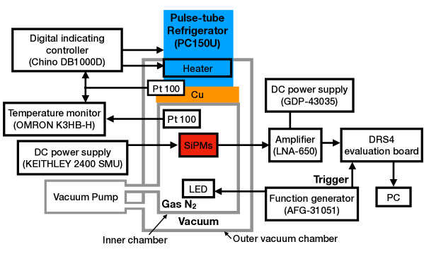
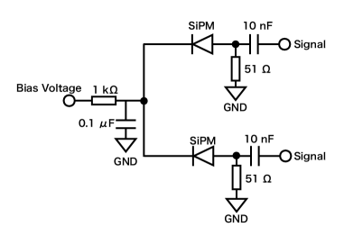
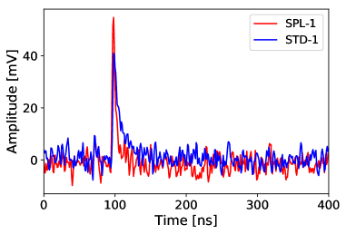
The experiment was performed in the Kamioka underground laboratory at a depth of approximately 1,000 meters. Figure 1 shows a block diagram of the setup that was used for this experiment. This setup consisted of an inner chamber filled with gas nitrogen along with an outer vacuum chamber. SiPMs were installed in the inner chamber and on a readout board, and the readout schematic is shown in figure 2, left. Voltage (Vbias) from a source meter (KEITHLEY 2400 Source Meter) was applied to the SiPMs. Signals were amplified with a low noise amplifier (RF Bay LNA-650) with a 50db gain and read out using a DRS4 evaluation board [28], which acquired data with a rate of 1 GS/s and a length of 1024 data points per time window. Square pulses from a function generator (Tektronix AFG-31051) were used to turn on an LED and trigger the data acquisition via the DRS4 board. We operated two SPLs labeled as SPL-1(-2) and two STDs labeled as STD-1(-2). Figure 2 (right), shows the typical waveforms of SPL-1 (STD-1) acquired with DRS4 at a temperature of 163 (164) K and bias voltages of 94.6 (60.0) V. The temperature was measured by two Pt-100 sensors and was controlled with a pulse-tube refrigerator (ULVAC CRYOGENICS PC150U) and a heater connected to a digital indicating controller (Chino DB1000D). We operated the setup at a temperature range of 153 K to 298 K, which was stable within 0.5 K during the measurements.
4 Measurements and Results
4.1 Gain vs voltages, breakdown voltage, and single photoelectron spectrum
To investigate the single p.e. gain, resolution, and breakdown voltage () properties of both SiPMs, we measured their responses to the blue light ( 375 nm) from an LED. The function generator inputs square pulses with a frequency of 460 Hz and width of 30 ns to the LED. We obtained 40,000 triggered events for each temperature and bias voltage. Figure 3 shows a pulse area spectrum of SPL-1 at a temperature of 163 K and a bias voltage of 94.6 V.
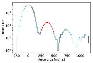
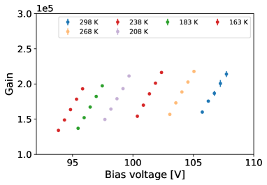
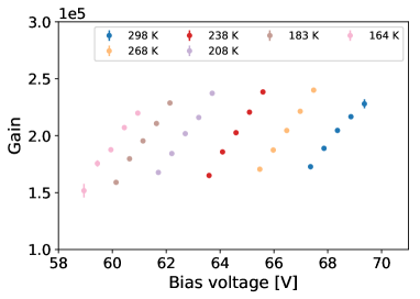
At this temperature, single p.e. gains of SPL-1 and STD-1 at a bias voltage of 94.6 V (SPL) and 60.0 V (STD) are estimated to be 1.6 105 and 2.0 105, respectively. The single p.e. resolutions () of SPL-1 and STD-1 are measured to be 17.9 % and 18.8 %, respectively, where () is mean (standard deviation) of the single p.e. pulse area obtained by fitting with Gaussian function as shown in figure 3. Figure 4 shows a single p.e. gain of SPL-1 and STD-1 as a function of bias voltage. The single p.e. gain () can be expressed as
| (4.1) |
where is a cell capacitance and is an electric charge. The slope of a linearly fitted function in figure 4 corresponds to . The cell capacitance of SPL-1 and STD-1 are estimated to be 4.3 fF at 163 K and 5.4 fF at 164 K, respectively.
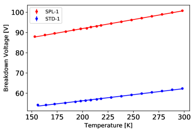
Breakdown voltage (), where the gain collapses to zero, is shown in figure 5 as a function of temperature. We can see from the figure 5 that of SPL-1 and STD-1 decrease with a slope of 88.3 mV/K and 61.2 mV/K, respectively. Also, approximately at the LXe temperature, of SPL-1 and STD-1 is estimated to be 88.8 V and 54.2 V, respectively.
Similar to low-field SiPMs developed by FBK [22], single p.e. gain of SPL is lower, and breakdown voltage and the slope in figure 5 of SPL is higher compared with STD. These observations can be explained by the fact that the depletion layer of SPL is thicker than that of STD as detailed in [22]. For all the characteristics described above, no significant sample dependence is observed.
4.2 Dark count rate and cross-talk probability
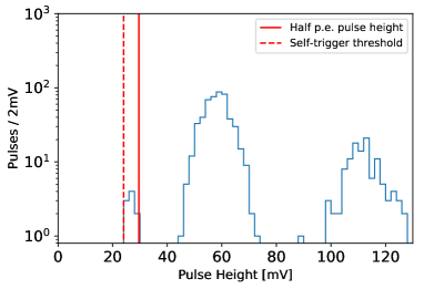
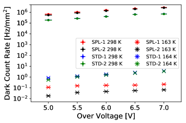
DCR is defined as the number of pulses per second whose height is larger than 0.5 p.e. In this study, it is normalized by the active area and the fill factor for each SiPMs. At a temperature between 198 K and 298 K, we acquired data with a random trigger because of high values of DCR. Below 198 K, data were obtained with a self-trigger with a threshold of 25 mV. Figure 6 (left) shows a pulse height distribution of SPL-1 at 163 K and an over-voltage of 6.0 V, where over-voltage is defined as . The peak around 60 mV corresponds to the mean of the single p.e. pulse height. A red dashed line in figure 6 shows the self-trigger threshold of 25 mV. The remaining noise contribution is discarded by requiring that pulse area is larger than . For the data acquired with self-trigger, deadtime of the DRS4 evaluation board ( 3 ) is taken into account when calculating the DCR. Figure 6 (right) shows DCRs for SPL and STD that are expressed as a function of over-voltage at temperatures of 298 K, 163 K(SPL), and 164 K(STD).
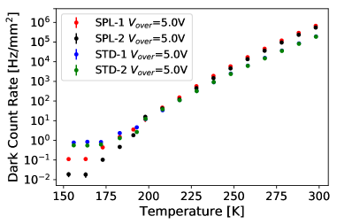
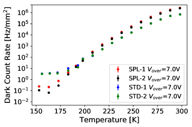
DCR, as a function of temperature is also shown in figure 7 at over-voltages of 5.0 V and 7.0 V, respectively. As discussed in section 2, between 200 K and 300 K, the contribution from thermally generated carriers is dominant; therefore, the DCR shows a rapid decrease with temperature. However, at temperatures below 200 K, the contribution from carriers originating from the band-to-band tunneling effect is dominant; therefore, the DCR has less temperature dependence. At room temperature, the DCR of SPL is found to be higher than that of STD. This can be originated from the fact that the depletion layer of SPL is thicker than that of SPL as discussed in section 4.1. The DCR for SPL-1(-2) at approximately 165 K is measured to be 0.11–0.24 (0.018–0.071) Hz/mm2 depending on over-voltage, less by a factor of 6–60 compared with that of STD, indicating that the modified inner field structure reduced the DCR.
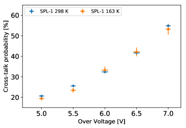
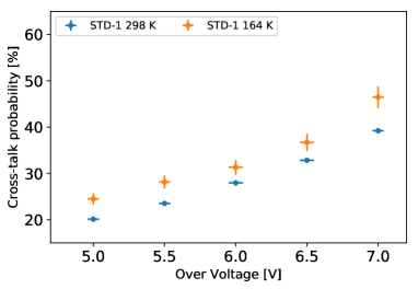
Cross-talk probability (CTP) is calculated as , where and are the number of pulses per second whose pulse heights are larger than 1.5 p.e. and 0.5 p.e., respectively [30]. Cross-talk occurs when multiplied electrons in a cell enter and fire a neighboring cell. Figure 8 shows the CTPs for SPL and STD at different temperatures as a function of over-voltage. It can be seen from the figure 8 that the CTP increases with over-voltage for both SiPMs. Moreover, the CTP of STD is found to increase with decreasing temperature. This is not well understood, but it can be because one of the cross-talk components, delayed cross-talk, has large temperature dependence as detailed in [31]. At approximately the LXe temperature and an over-voltage of 6.0 V, the CTPs of SPL-1 and STD-1 are estimated to be 33.4 % and 31.5 %, respectively. No significant sample differences in the CTP are observed.
5 Conclusion and Outlook
SiPM is a good candidate for photo-detectors in future dark matter experiments with LXe because of its low radioactivity. However, it has a high DCR, and it is necessary to reduce it at least to the same level as it is for the PMTs ( 0.01 Hz/mm2) used in LXe experiments [17]. Hamamatsu developed a dedicated SiPM (SPL) with the lowered electric field for suppressing the band-to-band tunneling effect, and we characterized it in a temperature range of 153–298 K. As a result, by modifying the inner electric field structure, the DCR at the LXe temperature could be reduced by a factor of 6–60 compared to that of STD that depended on over-voltage. Currently, both SPL and STD are not sensitive to the LXe scintillation light, but we are developing a dedicated SiPM sensitive to VUV light with the help of Hamamatsu. The DCR of S13370, a commercially available SiPM for VUV light detection, was measured to be 0.1–0.8 Hz/mm2 at the LXe temperature depending on over-voltage [16]. With the same technology developed in this work, it might be possible that the DCR of S13370 can be reduced to the same extent, enabling SiPMs to be used in future dark matter experiments using LXe.
Acknowledgments
We thank Hamamatsu Photonics K. K. for this fruitful collaboration and the production of the SiPMs used in this study. We gratefully acknowledge the cooperation of Kamioka Mining and Smelting Company. This work was supported by DAIKO FOUNDATION, Foundation of Kinoshita Memorial Enterprise, the Japanese Ministry of Education, Culture, Sports, Science and Technology, Grant-in-Aid for Scientific Research, JSPS KAKENHI Grant Number 19H05805 and 20H01931, and the joint research program of the Institute for Cosmic Ray Research (ICRR), the University of Tokyo.
Appendix A After-pulse probability
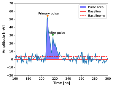
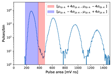
The doping density of SPL is lower than that of STD because of the lowered electric field strength, therefore SPL is expected to have lower after-pulse probability compared with STD. The number of carriers generated by the after-pulse process is less than that for single p.e., and an after-pulse signal generally piles up with a primary signal as shown in figure 9 since it is generated before the recovery time of the primary signal [32]. Therefore, a single p.e. with an after-pulse signal has a pulse area ranging between single p.e. and double p.e. Figure 10 (left) shows the pulse area distribution of SPL-1 at a temperature of 198 K and bias-voltage of 97.0 V. The first and second peaks correspond to the pulse area for single p.e. and double p.e., respectively. Pulses with after-pulses are contained in the red shaded region defined by [, ]. In this study, after-pulse probability () is defined as
| (A.1) |
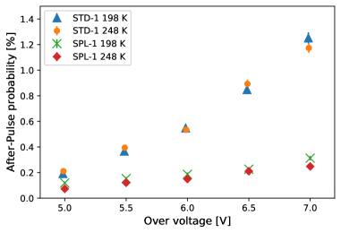
where () is the number of pulses contained in the red (blue) shaded region. Figure 10 (right) shows the after-pulse probability of SPL-1 and STD-1 as a function of over-voltage. As expected, the after-pulse probability of SPL is measured to be lower than that of STD, and no significant dependence on temperature has also been found.
Appendix B Photo-detection efficiency
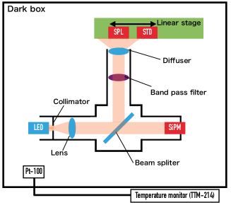
Since lowering the electric field strength can potentially reduce photo-detection efficiency (PDE), a comparison of PDE between STD and SPL has been done to investigate such an effect. Figure 11 (left) shows a setup to measure the relative PDE. Light emitted from an LED passes through a collimator with a diameter of 1 mm and a lens, and is then splitted with a beam splitter. The transmitted light illuminates the SiPM (Hamamatsu S13370-3050CS), and it is used to monitor the stability of the LED light. In this study, LED light level has been stable with 0.5 fluctuation. Reflected light passes through a band-pass filter and a diffuser, and then illuminates the SPL and STD. SPL and STD are mounted on x-y linear stage to control their positions remotely. Three LEDs with different wavelength of 405 nm, 470 nm, and 630 nm were used to investigate the wavelength dependence of PDE. Temperature inside the bark box was monitored with a Pt-100 sensor, and had been stable at 2971 K. The relative PDE in this study is calculated by
| (B.1) |
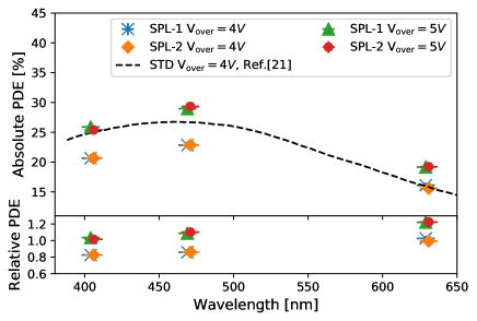
where is occupancy for each SiPMs estimated with the method detailed in [33]. The absolute PDE is then calculated by scaling the estimated relative PDE by the absolute PDE of STD at an over-voltage of 4 V provided by Hamamatsu [21]. Figure 11 (right) shows the measured (relative) PDE of SPL-1(-2) at over-voltages of 4 V and 5 V as a function of wavelength. As can be seen from the figure 11, no significant differences in the estimated PDE between SPL and STD are observed. The relative PDE is found to have a wavelength dependence. This can be originated from the fact that both SiPMs have different depth profiles, and thus the sensitivity to VUV light can be affected by lowering the internal electric field strength, resulting in a reduction of PDE. However, a dedicated VUV-sensitive SiPM with higher fill factor is planed to be developed by Hamamatsu, which should improve PDE [34].
References
- [1] E. Aprile et al. (XENON Collaboration), Dark Matter Search Results from a One Ton-Year Exposure of XENON1T, Phys. Rev. Lett. 121 111302 (2018).
- [2] X. Cui et al. (PandaX-II Collaboration), Dark Matter Results from 54-Ton-Day Exposure of PandaX-II Experiment, Phys. Rev. Lett. 119 181302 (2017).
- [3] D. S. Akerib et al. (LUX Collaboration), Results from a Search for Dark Matter in the Complete LUX Exposure, Phys. Rev. Lett. 118 021303 (2017).
- [4] K. Abe et al. (XMASS Collaboration), A direct dark matter search in XMASS-I, Physics Letters B 789 (2019) 45–53.
- [5] J. Aalbers et al. (DARWIN Collaboration), DARWIN: towards the ultimate dark matter detector, JCAP11 (2016) 017.
- [6] Ciaran A. J. O’Hare, Dark matter astrophysical uncertainties and the neutrino floor, Phys. Rev. D 94 063527 (2016).
- [7] K. Fujii et al., High-accuracy measurement of the emission spectrum of liquid xenon in the vacuum ultraviolet region, Nuclear Instruments and Methods in Physics Research Section A: Accelerators, Spectrometers, Detectors and Associated Equipment 795 (2015) 293-297.
- [8] E. Aprile et al. (XENON Collaboration), Lowering the radioactivity of the photomultiplier tubes for the XENON1T dark matter experiment, Eur. Phys. J. C 75 546 (2015).
- [9] K. Abe et al.(XMASS Collaboration), Development of low radioactivity photomultiplier tubes for the XMASS-I detector, Nuclear Instruments and Methods in Physics Research Section A: Accelerators, Spectrometers, Detectors and Associated Equipment, 922 (2019) 171–176.
- [10] E. Aprile et al. (XENON Collaboration), The XENON1T Dark Matter Experiments, Eur. Phys. J. C 77 881 (2017).
- [11] S. Ogawa et al. (MEG II Collaboration), Liquid xenon calorimeter for MEG II experiment with VUV-sensitive MPPCs, Nuclear Instruments and Methods in Physics Research Section A: Accelerators, Spectrometers, Detectors and Associated Equipment 845 (2017) 528–532.
- [12] F. Acerbi et al., Silicon photomultipliers: technology optimizations for ultraviolet, visible and near-infrared range, Instruments, 3(1), 15 (2019).
- [13] M. Capasso et al., FBK VUV-sensitive Silicon Photomultipliers for cryogenic temperatures, Nuclear Instruments and Methods in Physics Research Section A: Accelerators, Spectrometers, Detectors and Associated Equipment, 982, (2020), 164478.
- [14] Hamamatsu Photonics, https://www.hamamatsu.com/jp/ja/product/optical-sensors/mppc/mppcmppc-array/index.html
- [15] L. Baudis et al., Characterisation of Silicon Photomultipliers for Liquid Xenon Detectors, 2018 JINST 13 P10022.
- [16] G. Gallina et al., Characterization of the Hamamatsu VUV4 MPPCs for nEXO, Nuclear Instruments and Methods in Physics Research Section A: Accelerators, Spectrometers, Detectors and Associated Equipment, 940 (2019) 371–379.
- [17] P. Barrow et al., Qualification tests of the R11410-21 photomultiplier tubes for the XENON1T detector, 2017 JINST 12 P01024.
- [18] E. Aprile et al. (XENON Collaboration), The XENON1T data acquisition system, 2019 JINST 14 P07016.
- [19] E. Aprile et al. (XENON Collaboration), XENON1T dark matter data analysis: Signal and background models and statistical inference, Phys. Rev. D 99 112009.
- [20] J. Wulf, Direct Dark Matter Search with XENON1T and Developments for Multi-Ton Liquid Xenon Detectors, Ph.D thesis, Universität Zürich (2018).
- [21] Hamamatsu Photonics, https://www.hamamatsu.com/resources/pdf/ssd/s12572-010etckapd1045j.pdf
- [22] F. Acerbi et al., Cryogenic Characterization of FBK HD Near-UV Sensitive SiPMs, IEEE Transactions on Electron Devices, 64(2), 521-526 (2017).
- [23] G. A. M. Hurkx et al., A New Analytical Diode Model Including Tunneling and Avalanche Breakdown, IEEE Trans. Electron Devices 39 (1992) 2090–2098.
- [24] R. H. Haitz, Mechanisms Contributing to the Noise Pulse Rate of Avalanche Diodes, J. Appl. Phys. 36 (1965) 3123.
- [25] G. Collazuol et al., Studies of silicon photomultipliers at cryogenic temperatures, Nuclear Instruments and Methods in Physics Research Section A: Accelerators, Spectrometers, Detectors and Associated Equipment 628 (2011) 389–392.
- [26] M. Ghioni et al., Large-area low-jitter silicon single photon avalanche diodes, Quantum Sensing and Nanophotonic Devices V 6900 (2008) 267–279.
- [27] N. Serra et al., Experimental and TCAD Study of Breakdown Voltage Temperature Behavior in SiPMs, IEEE Transactions on Nuclear Science 583 (2011) 1233–1240.
- [28] PSI, DRS4 Evaluation Board, https://www.psi.ch/en/drs/evaluation-board
- [29] F. Acerbi et al., Understanding and simulating SiPMs, Nuclear Instruments and Methods in Physics Research Section A: Accelerators, Spectrometers, Detectors and Associated Equipment, 926 (2019) 16–35.
- [30] Hamamatsu Photonics, Opto-semiconductor Handbook, https://www.hamamatsu.com/resources/pdf/ssd/e03handbooksiapdmppc.pdf
- [31] A. N. Otte et al., Characterization of three high efficiency and blue sensitive silicon photomultipliers, Nuclear Instruments and Methods in Physics Research Section A: Accelerators, Spectrometers, Detectors and Associated Equipment, 846 (2017) 106–125.
- [32] F. Nagy et al., Afterpulse and delayed crosstalk analysis on a STMicroelectronics silicon photomultiplier, Nuclear Instruments and Methods in Physics Research Section A: Accelerators, Spectrometers, Detectors and Associated Equipment 759 (2014) 44-49.
- [33] R. Saldanha et al., Model independent approach to the single photoelectron calibration of photomultiplier tubes, Nuclear Instruments and Methods in Physics Research Section A: Accelerators, Spectrometers, Detectors and Associated Equipment 863 (2017) 35–46.
- [34] Hamamatsu Photonics, https://indico.cern.ch/event/818783/contributions/3598485/attachments/1951255/3239319/ 191026_CHEF2019_HPK.pdf