Coupling of Light and Mechanics in a Photonic Crystal Waveguide
Abstract
Observations of thermally driven transverse vibration of a photonic crystal waveguide (PCW) are reported. The PCW consists of two parallel nanobeams with a vacuum gap between the beams. Models are developed and validated for the transduction of beam motion to phase and amplitude modulation of a weak optical probe propagating in a guided mode (GM) of the PCW for probe frequencies far from and near to the dielectric band edge. Since our PCW has been designed for near-field atom trapping, this research provides a foundation for evaluating possible deleterious effects of thermal motion on optical atomic traps near the surfaces of PCWs. Longer term goals are to achieve strong atom-mediated links between individual phonons of vibration and single photons propagating in the GMs of the PCW, thereby enabling opto-mechanics at the quantum level with atoms, photons, and phonons. The experiments and models reported here provide a basis for assessing such goals, including sensing mechanical motion at the Standard Quantum Limit (SQL).
Recent decades have seen tremendous advances in the ability to prepare and control the quantum states of atoms, atom-like systems in the solid state, and optical fields in cavities and free space. However, the integration of these diverse elements to achieve efficient quantum information processing still faces diverse challenges, including the wide range of highly dissimilar physical systems (e.g., atoms, ions, solid-state defects, quantum dots) that could be utilized to realize heterogeneous systems for quantum logic, memory, and long-range coupling. Each of these systems has unique advantages, but they are disparate in their frequencies, their spatial modes, and the fields to which they couple. For example, the electronic degrees of freedom in atoms and atom-like defects typically respond at optical frequencies, while their spin degrees of freedom, which are suitable for long-term storage of quantum states, respond to microwave or radio frequencies. On the other hand, the transmission of quantum information over long distances at room temperature requires the use of telecom-band photons in single-mode optical fibers.
Beginning with the pioneering work in Refs. Braginsky et al. (2001); Rokhsari et al. (2005), mechanical systems have now been recognized as broadly applicable means for overcoming these disparities and transferring quantum states between different quantum degrees of freedom Hammerer et al. (2009a); Rabl et al. (2010, 2009); Hammerer et al. (2009b). This is because mechanical systems Aspelmeyer et al. (2014a) can be engineered to couple efficiently and coherently to many different systems and can possess very low damping, particularly when operated at cryogenic temperatures. To date, quantum effects have been observed in mechanical systems coupled to superconducting qubits (via piezoelectric coupling) O’Connell et al. (2010), optical photons Chan et al. (2011); Purdy et al. (2013a); Safavi-Naeini et al. (2012); Brooks et al. (2012); Safavi-Naeini et al. (2013); Purdy et al. (2013b), and microwave photons Teufel et al. (2011); Palomaki et al. (2013). Efficient coupling has also been demonstrated between mechanical oscillators and spins in various solid-state systems, although to date the mechanical components of these devices have operated in the classical regime Rugar et al. (2004); Hong et al. (2012); Kolkowitz et al. (2012); Arcizet et al. (2011); MacQuarrie et al. (2013); Teissier et al. (2014); Ovartchaiyapong et al. (2014).
In this manuscript we describe nascent efforts to utilize strong coupling of atoms, photons, and phonons in nanophotonic PCWs to create a new generation of capabilities for quantum science and technology. Our long-term goal is to use optomechanical systems operating in the quantum regime to realize controllable, coherent coupling between isolated, few-state quantum systems. In our case, the system will consist of atoms trapped along a photonic crystal waveguide (PCW) that interact strongly with photons propagating in the guided modes (GMs) of the PCW Chang et al. (2018). The mechanical structure of the PCW in turn supports phonons in its various eigenmodes of motion. While much has been achieved in theory and experiment for strong coupling of atoms and photons in nano-photonics, much less has been achieved (or even investigated) for the optical coupling of motion and light in the quantum regime for devices such as described in Refs. Chang et al. (2018); Lodahl et al. (2017).
A longstanding challenge for this work is to achieve the integration of ultracold atoms with nanophotonic devices. If this challenge were overcome, quantum motion could be harnessed to investigate enhanced nonlinear atom-light interactions with single and multiple atoms. New quantum phases Manzoni et al. (2017), novel mechanisms for controlling atoms near dielectric objects Chang et al. (2013), and strong atom-photon-phonon coupling Hammerer et al. (2009b) could be realized in the laboratory. Although difficult, this approach potentially benefits from several advantages when compared to conventional optomechanics, including (a) the extreme region of parameter space that atomic systems occupy (such as low mass and high mechanical Q factors), (b) the exquisite level of control and configurability of atomic systems, and (c) the pre-existing quantum functionality of atoms, including internal states with very long coherence times.
Of course, many spectacular advances of atomic physics already build upon these features Blatt and Wineland (2008); Haffner et al. (2008); Duan and Monroe (2010). On one hand, experiments with linear arrays of trapped ions achieve coherent control over phonons interacting with the ions’ internal states as pseudo spins. Goals that are very challenging for quantum optomechanics with nano- and micro-scopic masses, such as phonon-mediated entanglement of remote oscillators and single-phonon strong coupling, are routinely implemented with trapped ions. On the other hand, cavity QED with neutral atoms produces strong interactions between single photons and the internal states of single atoms or ensembles, leading to demonstrations of state mapping and atom-photon entanglement Reiserer and Rempe (2015).
What is missing thus far, and what motivates the initial steps described here, is a strong atom-mediated link between individual photons and phonons, to enable optomechanics at the quantum level. Initial steps described here include 1) observation and characterization of the low frequency, mechanical eigenmodes of an alligator photonic crystal waveguide (APCW) and 2) the development of theoretical models that are validated in the nontraditional regime in which our system works Shelby et al. (1985a, b), namely, well localized mechanical modes, but non-localized propagating photons both far from and near to the band edges of PCWs.
I The alligator photonic crystal waveguide
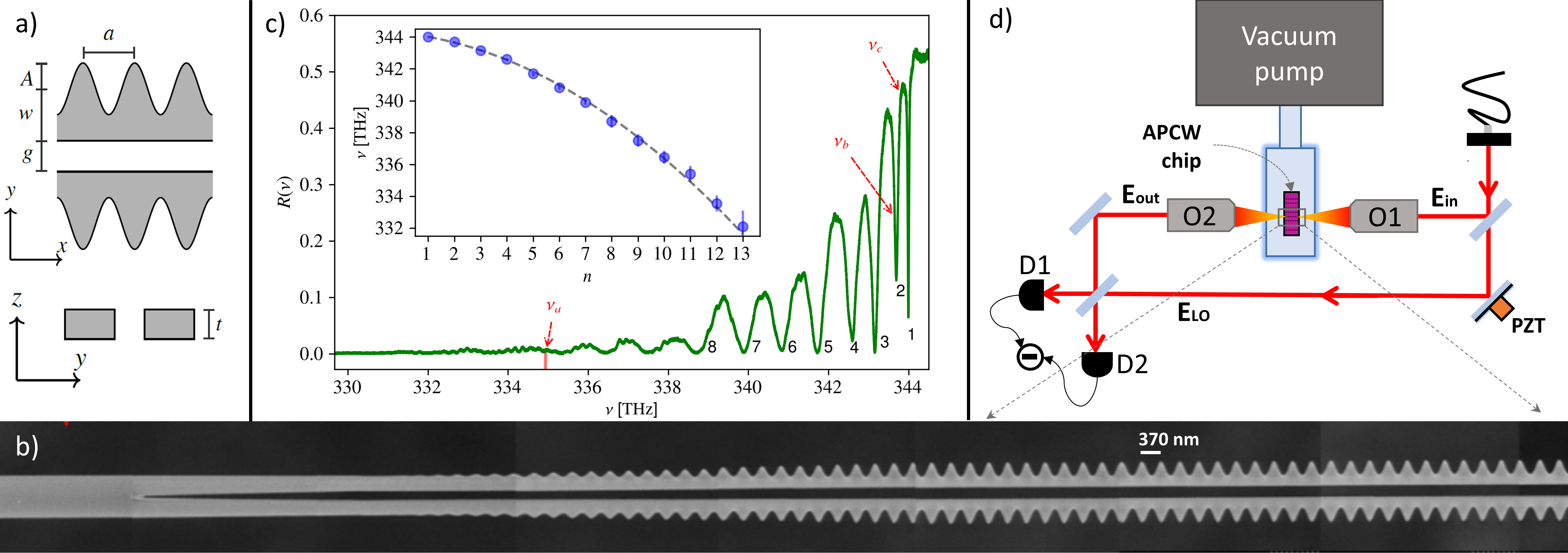
Figure 1 provides an overview of the APCW utilized in our experiments with details related to device fabrication and characterization provided in Refs. Yu et al. (2014a); Hood et al. (2016); Yu (2017); McClung (2017). The photonic crystal itself is formed by external sinusoidal modulation of two parallel nano-beams to create a photonic bandgap for TE modes with polarization predominantly along in Figure 1(a). The TE band edges have frequencies near the D1 and D2 transitions in atomic Cesium (Cs). Calculated and measured dispersion relations for such devices are presented in Ref Hood et al. (2016) where good quantitative agreement is found. Here, we focus on coupling of light and motion for TE modes of the APCW. TM modes of the APCW near the TE band edges resemble the guided modes of an unstructured waveguide.
As shown by the SEM image in Fig. 1(b), the APCW is connected to single-beam waveguides on both end and thereby freely suspended in the center of a 2 mm wide window in a Silicon chip. Well beyond the field of view in Fig. 1(b), a series of tethers are attached transversely to the single-beam waveguides along to anchor the waveguides to two side rails that run parallel to the axis of the device to provide thermal anchoring and mechanical support, with the coordinate system defined in Fig. 1(a). Important for our current investigation, the single-beam waveguides and the APCW itself are held in tension with .
Light is coupled into and out of TE guided modes of the APCW by a free-space coupling scheme that eliminates optical fibers within the vacuum envelope Béguin et al. (2020); Luan et al. (2020). An example of a reflection spectrum is given Fig. 1(c), which is acquired by way of light launched from and recollected by the microscope objective O1 shown in Fig. 1(d). Objectives O1, O2 are mode-matched to the fields to/from the terminating ends of the waveguide resulting in overall throughput efficiency from input objective O1 through the device with the APCW to output objective O2 for the experiments described here. The silicon chip itself contains a set of APCWs and is affixed to a small glass optical table inside a fused silica vacuum cell by way of silicate bonding Béguin et al. (2020); Luan et al. (2020).
II Observations of modulation spectra
With reference to Fig. 1(d), we have recorded spectra for the difference of photocurrents from detectors for light transmitted through an APCW for various probe frequencies below the frequency of the dielectric band edge. Here we employ a balanced homodyne scheme with and having identical optical frequency and each absent radio frequency modulation save that from propagation in the APCW. With free-space coupling to guided modes of the APCW, homodyne fringe visibility up to is obtained.
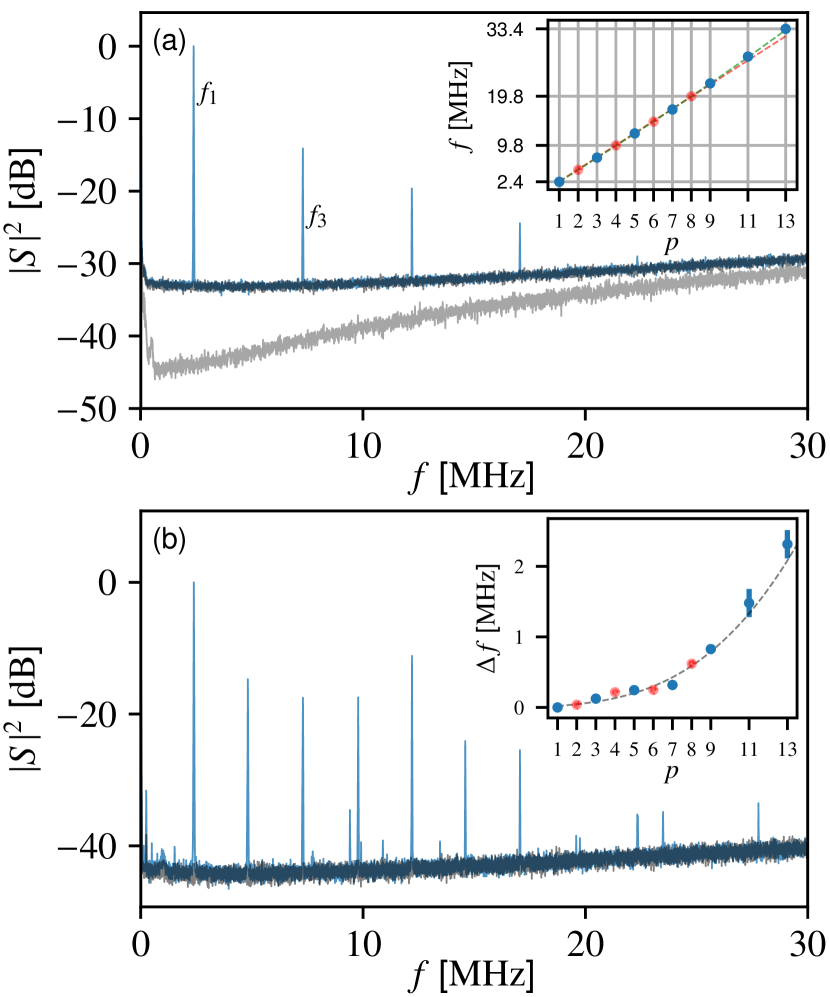
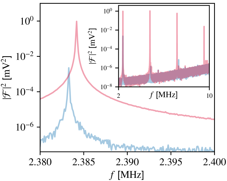
Measurement results for are displayed in Figures 2 and 3 for three optical frequencies (i.e., wavelengths ) moving from far below to near the dielectric band edge, as marked by red arrows in Figure 1c. The spectra display a series of narrow peaks and are of increasing complexity as the band edge is approached. All spectra are taken for a weak probe beam with power , while . The phase offset between and is set to maximize the observed spectral peaks whose frequencies exhibit only small shifts with changes in , as illustrated in Figure 9 in SM (2020). In vacuum () and at room temperature, the quality factor for the lowest peak at is . This value is compatible with the numerically predicted increase of the intrinsic from the high material pre-stress for thin SiN beams Villanueva and Schmid (2014).
An important feature of the spectra in Figure 2(a) is that peaks beyond occur at frequencies that are approximately odd harmonics of , with for . By contrast in Figure 2(b), the largest peaks double in number with now the presence of even harmonics of the fundamental frequency in addition to the odd harmonics from Figure 2(a). As shown by the inset in Figure 2(a), the dispersion relation is approximately linear with frequencies , where .
Further understanding emerges if we consider higher accuracy for the frequencies and examine the measured frequency differences as in the inset of Figure 2(b). Also plotted as the dashed line is the theoretical prediction for the mechanical frequency differences of a long, narrow, and thin beam, which is supported at hinged ends. For this model, the mechanical resonances are (Hocke et al., 2014)
| (1) |
where is the integer mode index, the Young’s modulus, the moment of inertia, the cross sectional beam area, the beam length, the mass density, and the beam stress.
Our APCW and connecting nano-beams are fabricated from SiN with high-tensile stress Yu et al. (2014b); Yu (2017). Together with the largely 1D geometry of the APCW (large aspect ratio of transverse to longitudinal dimension), the contribution of the bending term in can be neglected for the lowest order modes such that , giving rise to a close approximation of the linear dispersion of a tensioned string as in the inset to Figure 2(a). However, higher order modes have a clear quadratic contribution from the bending term that is evident in the inset to Figure 2(b).
In terms of absolute agreement between measured and predicted frequencies for the spectra in Fig. 2, from Eq. 1 we calculate a fundamental frequency from the total length , the manufacturer’s quoted tensile stress , and the mass density for LPCVD (stochiometric) Silicon Nitride (Pierson, 1999), . For the length , we consider the unit cells of the actual PCW region, plus the 30 tapered cells on each end, and finally the length from the beginning of the Y-split junction which separates the two corrugated beams. The devices are designed for small stress relaxation from that of the original SiN on Silicon chip Yu (2017). The predicted is close to the measured frequency .
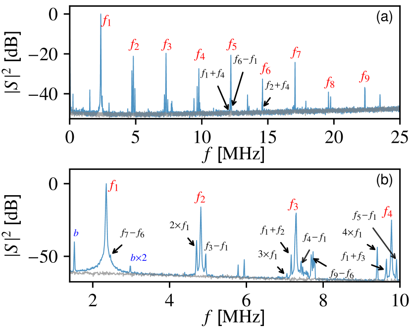
While the frequencies of the largest peaks in Figure 2 are well-described by Eq. 1, the complexity of the spectra increases as the band edge is approached with the appearance of many small satellite peaks as in Figure 3 for (i.e., wavelength ).
After labeling for clarity the dominant even and odd quasi-harmonics that also appear in Figure 2, we clearly observe a secondary series of integer harmonics in Figure 3, such as the second, third and fourth harmonics of the lowest frequency . The majority of the remaining peaks have frequencies which coincide with sums and differences of the main quasi-harmonics frequency components . Other peaks (e.g., at ) originate from unbalanced input laser light noise.
III Mechanical modes of the APCW
From measurements as in Figures 2 and 3 in hand and some understanding of the dispersion relation for the observed mechanical modes of the APCW, we turn next to more detailed characterization by way of numerical simulation. Principal goals are 1) to determine the mechanical eigenfunctions (and not just eigenfrequencies) associated with the observed modulation spectra and 2) to investigate the transduction mechanisms that convert mechanical motion of the various eigenfunctions to modulation of our probe beam. Beyond numerics to find the mechanical eigenmodes, we will present simple models to describe the transduction of mechanical motion to light modulation for various regimes far from and near to a band edge of the APCW. Quantitative numerical evaluation of the opto-mechanical coupling coefficient and eigenmodes for the full APCW structure will be presented in Section .
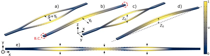
Figure 4 shows the fundamental mechanical modes of a small APCW structure obtained via numerical solution of the elastic equations. For clarity, we illustrate with a reduced geometry due to the large aspect ratio of our structure. The top panels represents the 3D deformed geometry as prescribed by the displacement vector field associated to each of the mechanical eigenmodes, with an arbitrary choice of mechanical energy. The displacement normalized to its maximum value is indicated by the colormap. The bottom panel displays a higher-order anti-symmetric mode with in the x-y plane for a longer structure
The design of the relatively long Y-junction arises from the need for efficient (i.e., adiabatic) conversion of the light guided from the single waveguide into the mode of the double-beam photonic crystal. While it does not represent a sharp boundary for the mechanics (please refer to refs. Yu (2017); McClung (2017) for details of full suspended structure with anchoring tethers), it does impose a symmetric termination geometry for both patterned beams. For the choice of effective two end-clamped boundary conditions, the four types of eigenmodes consist of two pairs of symmetric and antisymmetric oscillation, one pair with motion predominantly along , which we denote by , and the other with motion mainly along , denoted by and labelled by the mode number . For the actual full APCW structure, the eigenfrequencies for the fundamental modes are in the ratio .
While the modes in Figure 4 correspond to the mode families with lowest eigenfrequencies, at higher frequency other type of beam motion with mixed displacements appear. Also, as discussed in the conclusion, the APCW is a 1D phononic crystal. The eigenmodes shown in Figure 4 correspond roughly to those of two weakly coupled nanobeam oscillators. Regarding the accuracy of the choice of boundary condition, we note that the mechanical properties of the differential modes are little impacted by the length of the single beam beyond the merging point of the junction.
IV Mapping motion to optical modulation
IV.1 Optical frequencies far from a band edge
A simple model for the transduction of motion of the APCW nano-beams into optical modulation explains some of the key observations from the previous sections. First of all, for a fixed GM frequency input to the APCW, each mechanical eigenmode adiabatically modifies the band structure of the APCW and thereby the optical dispersion relation for GM propagation along with frequency relative to the case with no displacement from equilibrium. In our original designs of the APCW, we undertook extensive numerical simulations of the band structure for variations of all the dimensions shown in Fig. 1(a) Refs. Yu (2017); McClung (2017); Hood et al. (2016). Guided by these earlier investigations, we deduce that the largest change in band structure with low frequency motion as in Fig. 4 arises from variation of the gap width from displacements for the antisymmetric eigenmode illustrated in Figure 4 (a).
As suggested by Eq. 1, we then consider a string model with describing displacement at each point along , namely , with maximum displacement . Here, is the mechanical wave vector with subject to boundary conditions, which in the simplest case are with then eigenvalues for . Again, denotes the mechanical eigenmode in Fig. 4(a) and represents antisymmetric displacements of each nanobeam, with one beam of the APCW having displacement from equilibrium and the opposing beam with phase-coherent displacement , leading to a cyclic variation of the total gap width as described by along the -axis of the APCW. For small displacements and fixed frequency far from the band edge, we can then expand the dispersion relation to find , where , with .
Since displacements vary along as described by the particular mechanical eigenmode , will also vary along . The differential phase shift due to a mechanical eigenmode for propagation of an optical GM from input to output of the APCW is then given by (in our simple model) for odd, and for even. Here, is the differential phase shift between optical propagation through the APCW with and without mechanical motion (i.e., and ).
When driven by thermal Langevin forces, the mechanical mode oscillates principally along at frequency with rms amplitude , where as calculated in SM (2020). For small, thermally driven phase shifts, likewise oscillates predominantly at with rms amplitude linearly proportion to displacement, . Far from a band edge, both and should be Gaussian random variables, with for example, probability density .
IV.2 Measurements of phase and amplitude modulation
Overall, our simple model describes mechanical motion via eigenmodes that modifies the dispersion relation for an optical GM, which in turn leads to nonzero phase modulation at frequency for odd eigenmodes and zero phase modulation for even modes, precisely as observed in Fig. 2(a) far from the band edge. Here we present measurements to substantiate further this model.
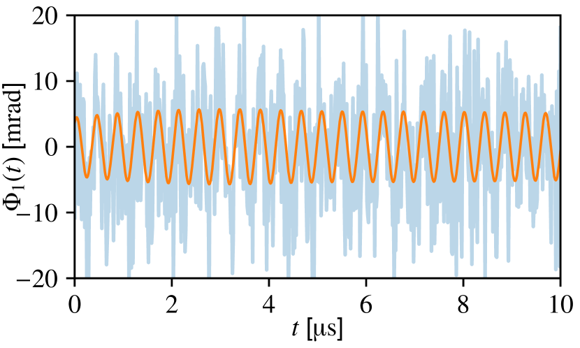
With reference to Fig. 1(d), the balanced homodyne detector enables measurement of an arbitrary phase quadrature by offset of the relative phase between the probe output field and the local oscillator field with set by adjusting the voltage of the piezoelectric mirror mount (PZT) shown in Fig. 1(d). Phase or amplitude modulation of the probe field is then unambiguously identified by offset for PM or for AM. By calibrating the low-frequency () fringe amplitude for the difference current of the balanced homodyne signal as a function of and then setting (i.e., at the zero-crossing of the interferometer fringe signal for highest phase sensitivity), we observe periodic variation in at , corresponding precisely to the lowest eigenfrequency in the phase imprinted on the probe from propagation through the APCW. Figure 5 displays an example of a single time trace for fixed clearly evidencing both for broad bandwidth detection and for processing with a digital bandpass filter centered at with bandpass.
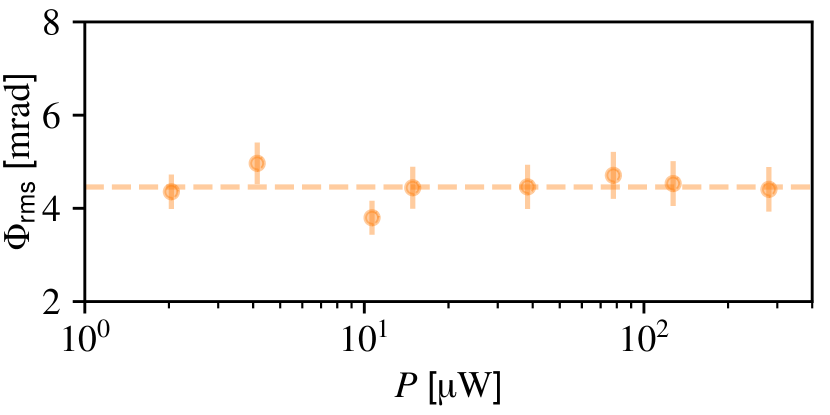
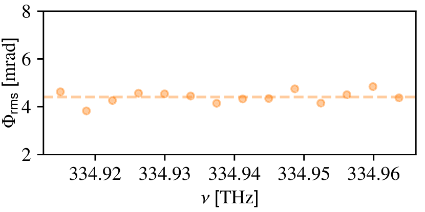
Over a range of probe powers (Fig. 10) and frequencies far from the band edge (Fig. 11), the typical observed rms amplitude of the detected phase modulation at is . This measured modulation for should be compared to the value predicted from our simple model. The thermally driven amplitude is calculated in SM (2020), and can be combined with a transduction factor inferred from band structure calculations to arrive to a predicted rms value for thermally driven phase modulation at frequency of about SM (2020). In Section we will address the origin of disparity between measured and modeled phase modulation by way of full numerical simulation for the APCW.
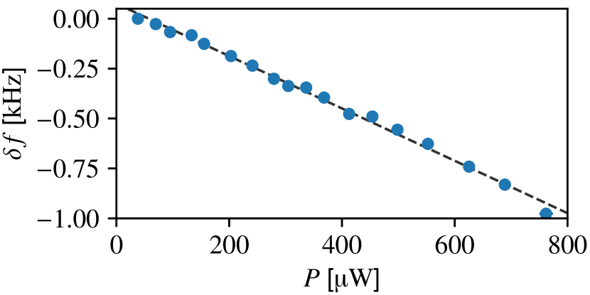
Note that we observe a shift of the mechanical frequency with guided probe power, which allows an inference of the bare mechanical frequency in the absence of probe light. Representative data for the power-dependent shift can be found in Fig. 9, which shows a linear decrease with probe power of with and . This shift with probe power is consistent with thermal expansion of the APCW due to absorption of probe power.
IV.3 Missing modes
There remains the question of ‘missing modes’. If indeed the dominant spectral peaks in Fig. 2 are associated with the eigenfunctions , what has become of the other three sets of eigenfunctions ? The answer provided by our simple model of mechanical motion modifying the dispersion relation is that is unique in producing a large first-order change in with displacement.
Figure 4 reveals that only has distinct geometries for displacements (i.e., the two nanobeams are more separated for and less separated for ) leading to a much larger calculated transduction factor for motion along than for motion along . Moreover, far from the band edge, the symmetric modes have small transduction factors comparable to those for modes of a single unmodulated nanobeam of the thickness and average width of the APCW. This issue is addressed in quantitative detail in Section with a full numerical simulation of optomechanical coupling for the APCW.
IV.4 Optical frequencies near a band edge
Near the band edge of a PCW, the mapping of mechanical motion to modification of an optical probe has a qualitatively distinct origin from that in the previous section for the dispersive regime of a PCW. For a finite length PCW, there appears a series of optical resonances with as displayed in Figure 1(c). Each optical resonance arises from the condition with at the band edge Hood et al. (2016); Hood (2017). The mapping from wave vector to frequency involves a nonlinear dispersion relation near the band edge, which for our devices takes the form
| (2) |
where () is the lower (upper) band edge frequency, and is a frequency related to the curvature of the band near the band edge. Validation of this model by measurement and numerical simulation is provided in Refs. Hood et al. (2016); Hood (2017).
For our current investigation, the lower frequency for which is the dielectric band edge frequency. We model how displacements of the APCW geometry for the various mechanical eigenmodes illustrated in Fig. 4 lead to variation of the parameters in Equation 2. Specifically, since the resonance condition involves only the effective length of the APCW (i.e., with the number of unit cells and lattice constant ), each optical resonance will be taken to have fixed with then the associated optical frequency changing due to variation of parameters in Eq. 2 driven by displacements from the mechanical eigenmodes.††
A mapping of changes in device geometry to changes in band edge frequencies is provided in Ref. McClung (2017). As in the previous subsection, we seek here a qualitative description to understand the complex transduction of mechanical motion to optical modulation in a PCW. Quantitative numerical calculations will be described in the next section.
That said, we proceed by way of Table 2.1 and Figure 2.13 in Ref. McClung (2017) to estimate the traditional optomechanical coupling coefficient for displacements at the optical resonance, , closest to the dielectric band edge at . Here, , where we consider change in resonant frequency due to variation of the gap width as from the simple model in the previous section, and where the factor arises for the eigenmode from the displacement for asymmetric motion of each beam by and . is the zero-point amplitude along the chosen coordinate SM (2020), with the effective mass of a 1D string and the mass corresponding to that of the APCW section plus half the mass of each taper. By way of the dispersion relation Eq. 2 and Ref. McClung (2017), we find that , and thus that the optomechanical coupling coefficient , which is to be compared to the value found in the following section for the full geometry.
V Numerical evaluation of the opto-mechanical coupling rate
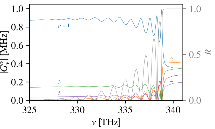
In this section, we consider the full APCW structure and evaluate numerically the opto-mechanical coupling rate from the waveguide to the band-edge regions. We first solve for the light field distribution propagating in the structure by launching the TE mode solution of the infinite single nanobeam waveguide section. This also gives reflection and transmission coefficients of the TE electromagnetic mode at both ends of the structure, with the reflection coefficient shown on the right axis of Fig. 6. We neglect the small imaginary part of the refractive index for SiN as well as losses due to fabrication imperfections. The mechanical eigenmodes are solved for the full structure (i.e., total number of unit cells for APCW , total number of taper cells , Y-split junction length ) with clamped ends, taking into account a constant stress distribution which is the steady-state stress field associated to the e-beam written geometry within the sacrificial layer of SiN with initial homogeneous in-plane stress .
Exploring SiN material properties within of the values provided by the wafer manufacturer, the numerically predicted mechanical frequencies are accurate to better than with measured frequencies for , and .
The exact expression for the opto-mechanical coupling rate due to displacement shifts of the dielectric boundaries within perturbation theory can be found in Johnson et al. (2002); SM (2020). It is given by the product of the mechanical zero-point motion amplitude , and the change in optical mode eigenfrequency due the dielectric displacement prescribed by the mechanical mode (generalized coordinate , SM (2020)), .
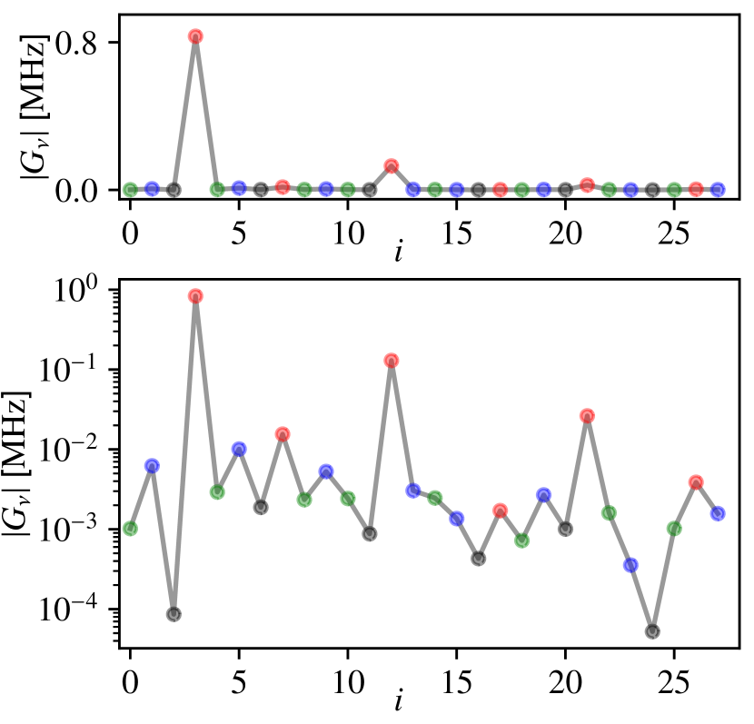
The values of the coupling rate are shown in Fig. 6 for various eigenmodes for the family as functions of optical frequency, where the actual eigenmode was approximated by a sine mode shape in Section IV. While the predicted is largest for such mode family, we report in supplemental Fig. 12 the simulated values for all low-frequency modes. The calculation spans from the waveguide regime far below the TE dielectric band edge, to then approaching the band edge, and finally into the band gap itself. The value of reaches up to at resonance near the band edge. This is slightly larger than predicted from the simple model in Section IV, which ignored the finite geometry with the Y-junction, tapered cells and narrowing of the physical gap (i.e., infinite APCW).
In contrast to the strains associated with -acoustic modes for some optomechanical systems Eichenfield et al. (2009a) that lead to photo-elastic contributions comparable to those from the dielectric moving boundaries, we find that the contribution is negligible (by several orders of magnitude) as compared to the dielectric moving boundary contribution for the long-wavelength vibrations under consideration for the APCW, for which the phonon wavelength becomes comparable to the optical wavelength. A measurement of the photo-elastic constant for SiN can be found in Gyger et al. (2020). Also note that , with the ratio of SiN (as here) to Si (as in Eichenfield et al. (2009a)) refractive indices .
To validate our numerical calculations, we have reproduced published results for several nanophotonic structures, Eichenfield et al. (2009b); Burek et al. (2016); Li et al. (2015), as discussed in the Supplemental Material.
Despite their relatively large effective mass (), the low frequency mechanical modes of the APCW achieve mass-frequency products and hence zero-point motion similar to that for 1D structures with microwave phonons coupled to a photonic defect light mode Eichenfield et al. (2009b). For comparison of the APCW with 2D structures (as in Tsaturyan et al. (2017)), the mechanical modes are in the few MHz domain in both cases, but have an effective mass which is two orders of magnitude larger () for the case.
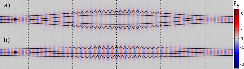
Beyond traditional perturbation theory which utilizes the unperturbed optical fields to evaluate , a powerful approach to confirm the transduction mechanism consists in solving Maxwell’s equations for the propagation of light in the deformed dielectric geometry at all phases of the prescribed mechanical eigenmode. Figure 7 illustrates this method, where the deformation of the dielectric produces a relative phase shift on the output light relative to the undeformed case. Owing to the large mismatch between optical and acoustic wave-vectors, the deformation is quasi-adiabatic. In particular for our very long structure and picometer thermal amplitude, radiation losses into non-guided modes are negligible. With this approach we anticipate weaker phase modulation for , and motions to occur at twice their respective eigenfrequency.
VI Conclusion and outlook
We have reported measurements and models that investigate the low frequency, thermally driven motion of the normal modes of an APCW and the transduction of this motion to the amplitude and phase of weak optical probe beams propagating in a TE guided mode both far from and near to the dielectric bandedge of the APCW. The in-plane antisymmetric mode of the two corrugated nanobeam oscillators dominates the opto-mechanical coupling to TE guided mode light. Simple models describe the basic transduction mechanisms both in the waveguide region far from a band edge as well as in a “cavity-like” regime for frequencies near a band edge.
Beyond simple models, full numerical simulations of the APCW structure have been carried out for quantitative predictions of optomechanical coupling as in Figure 6. An example is the prospect for detection of zero-point motion . Following the analysis in Ref. Clerk et al. (2010), we find probe power would be sufficient to reach phase sensitivity corresponding to for measurement bandwidth equal to the current linewidth for if this mode were cooled to its motional ground state. Moreover, the resulting back-action noise from the probe would correspond to , thereby reaching the Standard Quantum Limit for motion of the APCW at .
While the quality factors are modest for the APCW compared to current best literature values, the very small effective mass of the APCW allows for thermo-mechanical force sensitivity at a limit of . This value is only times larger than that of Tsaturyan et al. (2017) (), namely .
In terms of cooling to the ground state from a room-temperature APCW, the minimum -frequency product Wilson et al. (2009) would require values about larger than currently observed. Certainly, many advanced design strategies are available for increasing quality factors for a “next-generation” of PCWs Tsaturyan et al. (2017). In addition, low GM powers lead to strong pondermotive forces within the gap of the APCW that could potentially be harnessed to increase mechanical quality factors by by way of “optical springs” Ni et al. (2012). Beyond the focus of this article, we can excite selectively the observed mechanical modes with amplitude-modulated guided light at the specific observed frequencies. In fact, we also observe driving of the mechanical resonances with the external optical conveyor belt described in Burgers et al. (2019).
As for optical cooling of the APCW, our initial measurements related to opto-mechanics in a nonlinear regime suggest that efficient cooling might be achieved by operating near a bandedge. For example, as illustrated by Fig. 13 in SM (2020), we observe low-power bistable behavior marked with strong self-oscillation (near radian-phase modulation amplitude) for continuous GM power thresholds below . The large scale oscillations could originate from thermal effects of the APCW due to the GM light, which we are investigating. Alternatively, the bistable behavior and self-induced oscillates might arise from optical spring effects as described in Ref. Rokhsari et al. (2005). A double-well potential with two stable local minima can be developed when the GM power is sufficiently high Aspelmeyer et al. (2014a). The detailed mechanism of the large scale oscillations is beyond the scope of this paper, and will be investigated in our subsequent experiments. Related instabilities for blue cavity detunings are a hallmark of cooling for red detunings in conventional opto-mechanics in optical cavities Kippenberg and Vahala (2007).
The observations on mechanical modes of the APCW reported here are also important for assessing deleterious heating mechanisms for combining atom trapping in the vicinity of nano-photonic structures Zoubi and Hammerer (2016). While the symmetric modes lead to negligible modulations of the guided light as compared to motion, the guided light intensity distribution still follows the motion of the APCW structure in the laboratory frame. A simple estimate of heating limited trap lifetime due to trap-potential pointing instability can be obtained from the thermal position instability of at , with Clerk et al. (2010). This noise level corresponds to an energy-doubling time Savard et al. (1997) of order , at atom trap frequency . We are working on further simulations of heating rates with the complex motion of these dielectric structures for cold atom traps. Implementing feedback cooling with guided light could also mitigate limitations from operation at room-temperature Zhao et al. (2012).
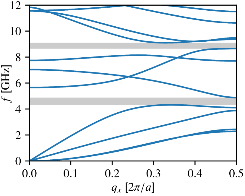
Although we have concentrated on low-frequency eignmodes of the APCW in the MHz regime, we have also investigated eigenmodes in the GHz regime that are of interest for many of the topics addressed here. As illustrated in Fig. 8, the corrugated structure of the APCW can lead to phononic band gaps in the GHz acoustic domain. The possibilities for band-gap engineering for both photons and phonons Eichenfield et al. (2009b) for application to atomic physics (e.g., for coupling mechanics to both Zeeman and hyperfine atomic states) represent an exciting frontier beyond the work reported here. One example to note is that the curvature of phonon bands can strongly enhance heating rates for atom traps Hümmer et al. (2019), which might offer new possibilities for engineering better atom traps in PCWs for atomic physics.
Acknowledgements.
The authors acknowledge sustained and important interactions with A. P. Burgers, L. S. Peng, and S.-P. Yu, who fabricated the nano-photonic structures used for this research. JBB acknowledges enlightening discussions with Y. Tsaturyan. HJK acknowledges funding from the Office of Naval Research (ONR) Grant #N00014-16-1-2399, the ONR MURI Quantum Opto-Mechanics with Atoms and Nanostructured Diamond Grant #N00014-15-1-2761, the Air Force Office of Scientific Research MURI Photonic Quantum Matter Grant #FA9550-16-1-0323, and the National Science Foundation (NSF) Grant #PHY-1205729.Appendix A Supporting figures
Figures 9, 10, 11, 12, and 13 provide supporting information for the measurements and numerical models presented in the main manuscript.
Appendix B Zero-point and thermal amplitudes
Following existing definitions for optomechanical crystal devices as in Eichenfield et al. (2009b), the amplitude of the displacement vector field u is parametrized by a generalized coordinate such that where is the unit-normalized displacement vector field with . From our full Comsol simulations, we find the maximum gap width is for motion.
The amplitude of zero-point motion of mode is Aspelmeyer et al. (2014a, b))
where is the mechanical angular frequency, and is the effective mass with the associated definition
where is the scalar mass density of the material.
From the numerical solution of the fundamental () mechanical mode, and . Note that the bulk mass of the simulated structure is .
At room temperature , , hence the mean thermal phonon number . This gives an rms thermal amplitude .
Equipartition theorem: The same result is obtained from the classical equipartition theorem. The rms amplitude of mode in thermal equilibrium at temperature is
Simple model: For the simple model, we consider the material mass corresponding to the full APCW section plus half the mass of each taper. With the normalization of the simplified eigenmode in section IV, the effective mass associated to the amplitude is , where a factor arises from the sinusoidal mode shape function (1D string) and a factor from being the maximum separation between the two nano-beams. When excited by Langevin thermal forces, the mechanical mode will oscillate along at frequency with rms amplitude
with and .
Estimates for the transduction of motion to modulation for the simplified eigenmode are derived from Fig. 2.13 in McClung (2017) and Eq. (2) in Section IV (D).
Appendix C Opto-mechanical coupling , Data processing, and Validation of simulations
Opto-mechanical coupling rate: , with (Ref. Johnson et al. (2002))
where u is the displacement vector field, n is the unit vector normal to the surface of the dielectric structure, and are the unperturbed electric and electric displacement fields (with components parallel or perpendicular to the local surface), and .
Data filter: For the measurement reported in Fig. 5, the photocurrent signal is sampled every with a precision digital oscilloscope. The data are further processed with a fourth-order Butterworth bandpass filter with high-cut and low-cut frequencies .
Validation of numerical simulations: To validate the numerical predictions for our structure, we find excellent agreement with simulations performed on nanophotonic structures published from other research groups. (FEM simulations are performed with Comsol Multiphysics 5.4.). For instance, for the diamond crystal cavity with triangular beam cross-section in Burek et al. (2016), we find for the flapping mode with ; for the swelling mode with .
References
- Braginsky et al. (2001) V. Braginsky, S. Strigin, and S. Vyatchanin, Physics Letters A 287, 331 (2001).
- Rokhsari et al. (2005) H. Rokhsari, T. J. Kippenberg, T. Carmon, and K. J. Vahala, Optics Express 13, 5293 (2005).
- Hammerer et al. (2009a) K. Hammerer, M. Aspelmeyer, E. S. Polzik, and P. Zoller, Physical Review Letters 102, 020501 (2009a).
- Rabl et al. (2010) P. Rabl, S. J. Kolkowitz, F. H. L. Koppens, J. G. E. Harris, P. Zoller, and M. D. Lukin, Nature Physics 6, 602 (2010).
- Rabl et al. (2009) P. Rabl, P. Cappellaro, M. V. G. Dutt, L. Jiang, J. R. Maze, and M. D. Lukin, Physical Review B 79, 041302 (2009).
- Hammerer et al. (2009b) K. Hammerer, M. Wallquist, C. Genes, M. Ludwig, F. Marquardt, P. Treutlein, P. Zoller, J. Ye, and H. J. Kimble, Phys. Rev. Lett. 103, 063005 (2009b).
- Aspelmeyer et al. (2014a) M. Aspelmeyer, T. J. Kippenberg, and F. Marquardt, Rev. Mod. Phys. 86, 1391 (2014a).
- O’Connell et al. (2010) A. D. O’Connell, M. Hofheinz, M. Ansmann, R. C. Bialczak, M. Lenander, E. Lucero, M. Neeley, D. Sank, H. Wang, M. Weides, J. Wenner, J. M. Martinis, and A. N. Cleland, Nature 464, 697 (2010).
- Chan et al. (2011) J. Chan, T. P. M. Alegre, A. H. Safavi-Naeini, J. T. Hill, A. Krause, S. Gröblacher, M. Aspelmeyer, and O. Painter, Nature 478, 89 (2011).
- Purdy et al. (2013a) T. P. Purdy, R. W. Peterson, and C. A. Regal, Science 339, 801 (2013a).
- Safavi-Naeini et al. (2012) A. H. Safavi-Naeini, J. Chan, J. T. Hill, T. P. M. Alegre, A. Krause, and O. Painter, Physical Review Letters 108, 033602 (2012).
- Brooks et al. (2012) D. W. C. Brooks, T. Botter, S. Schreppler, T. P. Purdy, N. Brahms, and D. M. Stamper-Kurn, Nature 488, 476 (2012).
- Safavi-Naeini et al. (2013) A. H. Safavi-Naeini, S. Gröblacher, J. T. Hill, J. Chan, M. Aspelmeyer, and O. Painter, Nature 500, 185 (2013).
- Purdy et al. (2013b) T. P. Purdy, P.-L. Yu, R. W. Peterson, N. S. Kampel, and C. A. Regal, Physical Review X 3, 031012 (2013b).
- Teufel et al. (2011) J. D. Teufel, T. Donner, D. Li, J. W. Harlow, M. S. Allman, K. Cicak, A. J. Sirois, J. D. Whittaker, K. W. Lehnert, and R. W. Simmonds, Nature 475, 359 (2011).
- Palomaki et al. (2013) T. A. Palomaki, J. D. Teufel, R. W. Simmonds, and K. W. Lehnert, Science 342, 710 (2013).
- Rugar et al. (2004) D. Rugar, R. Budakian, H. J. Mamin, and B. W. Chui, Nature 430, 329 (2004).
- Hong et al. (2012) S. Hong, M. S. Grinolds, P. Maletinsky, R. L. Walsworth, M. D. Lukin, and A. Yacoby, Nano Letters 12, 3920 (2012).
- Kolkowitz et al. (2012) S. Kolkowitz, A. C. B. Jayich, Q. P. Unterreithmeier, S. D. Bennett, P. Rabl, J. G. E. Harris, and M. D. Lukin, Science 335, 1603 (2012).
- Arcizet et al. (2011) O. Arcizet, V. Jacques, A. Siria, P. Poncharal, P. Vincent, and S. Seidelin, Nature Physics 7, 879 (2011).
- MacQuarrie et al. (2013) E. R. MacQuarrie, T. A. Gosavi, N. R. Jungwirth, S. A. Bhave, and G. D. Fuchs, Physical Review Letters 111, 227602 (2013).
- Teissier et al. (2014) J. Teissier, A. Barfuss, P. Appel, E. Neu, and P. Maletinsky, Physical Review Letters 113, 020503 (2014).
- Ovartchaiyapong et al. (2014) P. Ovartchaiyapong, K. W. Lee, B. A. Myers, and A. C. B. Jayich, Nature Communications 5, 4429 (2014).
- Chang et al. (2018) D. Chang, J. Douglas, A. González-Tudela, C.-L. Hung, and H. Kimble, Rev. Mod. Phys. 90, 031002 (2018).
- Lodahl et al. (2017) P. Lodahl, S. Mahmoodian, S. Stobbe, A. Rauschenbeutel, P. Schneeweiss, J. Volz, H. Pichler, and P. Zoller, Nature 541, 473 (2017).
- Yu et al. (2014a) S.-P. Yu, J. Hood, J. Muniz, M. Martin, R. Norte, C.-L. Hung, S. M. Meenehan, J. D. Cohen, O. Painter, and H. Kimble, Appl. Phys. Lett. 104, 111103 (2014a).
- Hood et al. (2016) J. D. Hood, A. Goban, A. Asenjo-Garcia, M. Lu, S.-P. Yu, D. E. Chang, and H. J. Kimble, Proc. Natl. Acad. Sci. U.S.A. 113, 10507 (2016).
- Yu (2017) S.-P. Yu, Nano-photonic platform for atom-light interaction, Ph.D. thesis, California Institute of Technology (2017).
- McClung (2017) A. C. McClung, Photonic crystal waveguides for integration into an atomic physics experiment, Ph.D. thesis, California Institute of Technology (2017).
- Manzoni et al. (2017) M. T. Manzoni, L. Mathey, and D. E. Chang, Nature Communications 8, 14696 (2017).
- Chang et al. (2013) D. E. Chang, K. Sinha, J. M. Taylor, and H. J. Kimble, Nat. Commun. 5 (2013), 10.1038/ncomms5343.
- Blatt and Wineland (2008) R. Blatt and D. Wineland, Nature 453, 1008 (2008).
- Haffner et al. (2008) H. Haffner, C. F. Roos, and R. Blatt, Physics Reports 469, 155 (2008).
- Duan and Monroe (2010) L.-M. Duan and C. Monroe, Rev. Mod. Phys. 82, 1209 (2010).
- Reiserer and Rempe (2015) A. Reiserer and G. Rempe, Rev. Mod. Phys. 87, 1379 (2015).
- Shelby et al. (1985a) R. M. Shelby, M. D. Levenson, and P. W. Bayer, Physical Review B 31, 5244 (1985a).
- Shelby et al. (1985b) R. M. Shelby, M. D. Levenson, and P. W. Bayer, Physical Review Letters 54, 939 (1985b).
- Béguin et al. (2020) J.-B. Béguin, A. P. Burgers, X. Luan, Z. Qin, S. P. Yu, and H. J. Kimble, Optica 7, 1 (2020).
- Luan et al. (2020) X. Luan, J.-B. Béguin, A. P. Burgers, Z. Qin, S.-P. Yu, and H. J. Kimble, Advanced Quantum Technologies n/a, 2000008 (2020).
- SM (2020) “See supplemental material,” (2020).
- Villanueva and Schmid (2014) L. G. Villanueva and S. Schmid, Physical Review Letters 113, 227201 (2014).
- Hocke et al. (2014) F. Hocke, M. Pernpeintner, X. Zhou, A. Schliesser, T. J. Kippenberg, H. Huebl, and R. Gross, Applied Physics Letters 105, 133102 (2014).
- Yu et al. (2014b) S.-P. Yu, J. D. Hood, J. A. Muniz, M. J. Martin, R. Norte, C.-L. Hung, S. M. Meenehan, J. D. Cohen, O. Painter, and H. J. Kimble, Applied Physics Letters 104, 111103 (2014b).
- Pierson (1999) H. Pierson, Handbook of chemical vapor deposition (CVD) : principles, technology, and applications (Elsevier, 1999).
- Hood (2017) J. D. Hood, Atom-light interactions in a photonic crystal waveguide, Ph.D. thesis, California Institute of Technology (2017).
- Johnson et al. (2002) S. G. Johnson, M. Ibanescu, M. A. Skorobogatiy, O. Weisberg, J. D. Joannopoulos, and Y. Fink, Phys. Rev. E 65, 066611 (2002).
- Eichenfield et al. (2009a) M. Eichenfield, J. Chan, A. H. Safavi-Naeini, K. J. Vahala, and O. Painter, Optics Express 17, 20078 (2009a).
- Gyger et al. (2020) F. Gyger, J. Liu, F. Yang, J. He, A. S. Raja, R. N. Wang, S. A. Bhave, T. J. Kippenberg, and L. Thévenaz, Phys. Rev. Lett. 124, 013902 (2020).
- Eichenfield et al. (2009b) M. Eichenfield, J. Chan, R. M. Camacho, K. J. Vahala, and O. Painter, Nature 462, 78 (2009b).
- Burek et al. (2016) M. J. Burek, J. D. Cohen, S. M. Meenehan, N. El-Sawah, C. Chia, T. Ruelle, S. Meesala, J. Rochman, H. A. Atikian, M. Markham, D. J. Twitchen, M. D. Lukin, O. Painter, and M. Lončar, Optica 3, 1404 (2016).
- Li et al. (2015) Y. Li, K. Cui, X. Feng, Y. Huang, Z. Huang, F. Liu, and W. Zhang, Journal of Optics 17, 045001 (2015).
- Tsaturyan et al. (2017) Y. Tsaturyan, A. Barg, E. S. Polzik, and A. Schliesser, Nature Nanotechnology 12, 776 (2017).
- Clerk et al. (2010) A. A. Clerk, M. H. Devoret, S. M. Girvin, F. Marquardt, and R. J. Schoelkopf, Rev. Mod. Phys. 82, 1155 (2010).
- Wilson et al. (2009) D. J. Wilson, C. A. Regal, S. B. Papp, and H. J. Kimble, Physical Review Letters 103, 207204 (2009).
- Ni et al. (2012) K.-K. Ni, R. Norte, D. J. Wilson, J. D. Hood, D. E. Chang, O. Painter, and H. J. Kimble, Physical Review Letters 108, 214302 (2012).
- Burgers et al. (2019) A. P. Burgers, L. S. Peng, J. A. Muniz, A. C. McClung, M. J. Martin, and H. J. Kimble, Proceedings of the National Academy of Sciences 116, 456 (2019).
- Kippenberg and Vahala (2007) T. J. Kippenberg and K. J. Vahala, Optics Express 15, 17172 (2007).
- Zoubi and Hammerer (2016) H. Zoubi and K. Hammerer, Phys. Rev. A 94, 053827 (2016).
- Savard et al. (1997) T. A. Savard, K. M. O’Hara, and J. E. Thomas, Phys. Rev. A 56, R1095 (1997).
- Zhao et al. (2012) Y. Zhao, D. J. Wilson, K.-K. Ni, and H. J. Kimble, Optics Express 20, 3586 (2012).
- Hümmer et al. (2019) D. Hümmer, P. Schneeweiss, A. Rauschenbeutel, and O. Romero-Isart, Phys. Rev. X 9, 041034 (2019).
- Aspelmeyer et al. (2014b) M. Aspelmeyer, T. J. Kippenberg, and F. Marquardt, Cavity optomechanics: nano-and micromechanical resonators interacting with light (Springer, 2014).