Disorder information from conductance: a quantum inverse problem
Abstract
It is straightforward to calculate the conductance of a quantum device once all its scattering centers are fully specified. However, to do this in reverse, i.e., to find information about the composition of scatterers in a device from its conductance, is an elusive task. This is particularly more challenging in the presence of disorder. Here we propose a procedure in which valuable compositional information can be extracted from the seemingly noisy spectral conductance of a two-terminal disordered quantum device. In particular, we put forward an inversion methodology that can identify the nature and respective concentration of randomly-distributed impurities by analyzing energy-dependent conductance fingerprints. Results are shown for graphene nanoribbons as a case in point using both tight-binding and density functional theory simulations, indicating that this inversion technique is general, robust and can be employed to extract structural and compositional information of disordered mesoscopic devices from standard conductance measurements.
Structures whose dimensions are comparable to or smaller than the electronic mean free path display transport features not associated with the classical ohmic behaviour [1]. These are quantum features found by solving the Schrödinger equation once the system Hamiltonian is known. Indeed, it is straightforward to describe how current flows in a quantum device by calculating its conductance once all scattering centres are specified. However, to do this in reverse, i.e., to find information about scatterers in a quantum device by simply looking at its conductance is rather challenging. This is a kind of Inverse Problem (IP) which consists of obtaining from a set of observations the causal factors that generated them in the first place. IP are intrinsic parts of numerous visualization tools [2, 3, 4, 5] but are not as common in the quantum realm, and even less so in the presence of disorder.
Disorder makes the description of the impurity potential by inverse scattering methods quite a daunting task. Multiple scattering depends on the scatterers’ locations and therefore likely to affect the electronic dynamics in seemingly unpredictable ways. To make matters worse theory shows that quantum interference in chaotic [6] and/or diffusive systems [7] gives rise to fluctuations whose statistical properties are universal, i.e. system independent, indicating that standard IP methods are neither practical nor useful in such situations.
Here we give a different twist to quantum IP approaches and demonstrate that, instead of detrimental, disorder may be actually beneficial to extracting information about scattering centres in a quantum device. In particular, we focus on the energy-dependent conductance of a quantum system, hereafter referred to as the conductance spectrum, which will serve as the only input of the inversion procedure described here. This is a quantity normally obtained by standard experimental setups of a gated two-terminal device but may also be found by calculation once the underlying Hamiltonian is fully specified. Here we introduce our inversion methodology by using the latter as a proxy for the former, i.e, calculated conductance spectra representing their experimental equivalent. The advantage of using calculated input functions is that we can refer back to the Hamiltonian that generated them in the first place, making it possible to assess the success of the inversion procedure.
Let us start by defining the system to be used throughout the manuscript. It consists of two electrodes separated by a scattering region of length and width , as illustrated in Fig. 1(a), a rather typical setup of electronic transport. The distinction between the leads and the central region is that the latter contains impurities as scattering centres [8]. In the linear response regime, the Landauer conductance reads , where is the Fermi distribution and is the dimensionless conductance (or transmission) given by [9, 10]
| (1) |
Here ( is the full retarded (advanced) Green function and () is the line width function accounting for the injection and lifetime of states in the left (right) contact. For simplicity, we consider the zero-temperature limit . Thermal corrections will be shown to have little effect on our procedure.
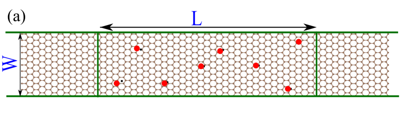
The expression for in Eq. (1) is model-independent, i.e., once the Hamiltonian is known one can find the corresponding Green function and obtain the energy dependent conductance of the system [9]. We focus on systems with relatively simple electronic structures, namely graphene nanoribbons (GNR). Although not an essential requirement, it helps to illustrate the methodology since GNR are well described by the tight-binding model [11, 12]. In this case the nearest-neighbour hopping and the on-site energies fully define the electronic structure of the nanoribbon. Fig. 1(b) shows the energy-dependent conductance for an armchair-edged GNR of width , Å being the graphene lattice parameter. The dashed line is the conductance spectrum for the pristine GNR. Results are shown for positive energies knowing that .
We now introduce substitutional impurities. It is convenient to express the impurity number also as the percentage concentration defined as , where is the total number of sites in the central region. Both and will be used interchangeably. The scattering strength of the impurities is characterized by the contrast between their on-site potential relative to that of the host, chosen to be zero. The solid line of Fig. 1(b) shows the conductance for the GNR with impurities, and unit cells (). Impurity locations were randomly selected but kept fixed in the underlying Hamiltonian that generated the conductance of Fig. 1(b).
Being the conductance sensitive to the locations of scattering centres, it is difficult to devise an inversion tool capable of spatially mapping all impurities from the conductance spectrum information alone. The brute-force method of comparing the input conductance with those of every possible disorder configuration is not viable because the number of combinations is too large for any practical situation. Machine-learning strategies are currently being attempted to overcome this combinatorial hurdle [13, 14, 15, 16, 17, 18, 19, 20] but spatial mapping of quantum devices through inversion remains challenging.
Nevertheless, given the conductance spectrum of a device, one might ask whether it is possible to find the exact number of scattering centres in it. This may not reveal the position of every impurity but it is a valuable piece of information and a lot more feasible to obtain. While the brute-force approach remains impractical, we must account for as many disorder realizations as possible. We define the configurationally averaged (CA) conductance by summing over realizations with the same number of impurities (or concentration ), i.e.,
| (2) |
where labels the different configurations. See SM [21] for a discussion on the suitable choices for .
The deviation between an arbitrary conductance result and its CA counterpart is given by
| (3) |
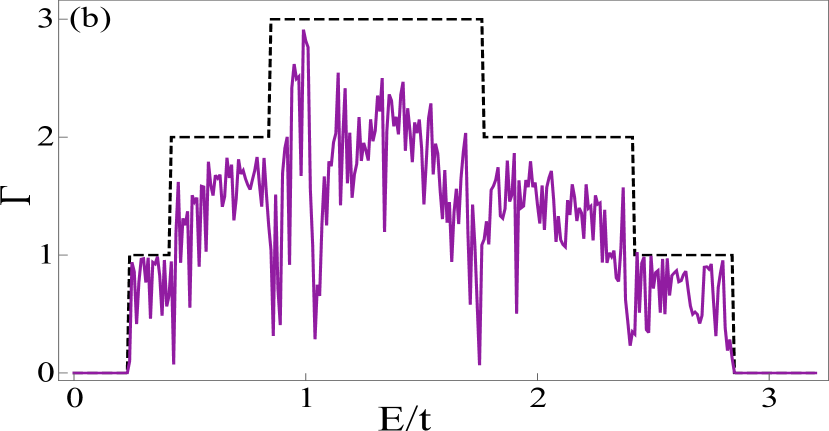
We reiterate that acts as the input conductance spectrum of a single realization and represents the immutable conductance of the device under investigation. The CA conductance spectrum, on the other hand, reflects the contribution of very many configurations and depends, in addition, on the impurity concentration. By treating as a variable parameter, we can look for minimization trends in that might indicate the real concentration in the device. Unfortunately, when plotted as a function of in Fig. 2(a), the deviation for a fixed energy is featureless with wide error bars that result from repeating the calculation 1000 times.
However, much cleaner trends are seen when is used in the form of a functional that measures how good a match and are. This quantity is the misfit function defined as
| (4) |
where and establish the energy window over which the integration takes place. Fig. 2(b) shows as a function of and displays a more distinctive trend with smaller error bars. The plot indicates that there is a sweet spot in impurity concentration for which the integrated deviation is minimal. Remarkably, this agrees with the actual number of impurities used in the calculation of , shown as a vertical (red) dashed line in the lower part of Fig. 2(b). Such a coincidence suggests that it might be possible to use as an inversion tool to find the number of impurities in a quantum device from simple conductance measurements. Note that no prior knowledge of the actual number of impurities was necessary to identify the misfit-function minimum.
To demonstrate that the agreement between the minimizing concentration of and the actual impurity concentration is not a fortuitous coincidence, we proceed to write the CA conductance [10] to linear order in
| (5) |
where is the derivative of with respect to evaluated at . The misfit function will naturally develop a minimum at , where
| (6) |
The vertical (black) dotted line shown on the upper part of Fig. 2(b) indicates the value of . Note that both the dotted and dashed lines are aligned, i.e., coincides not only with the actual concentration but also with the impurity concentration that minimizes . In fact, is an excellent approximation up to 3% impurity concentration and provides a simple yet accurate way of identifying the misfit function minimum. 111An alternative definition of , shown in the SM [21], may extend the validity of the approximation to up to 7%.
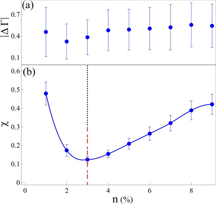
Besides the impurity concentration, other degrees of freedom can be added to the IP in question. Let us now consider an arbitrary sample conductance but this time assume that nothing is known about the impurity, i.e., neither its concentration nor its on-site potential . In this case, the input is simply treated as the conductance of a system with an unknown number of unspecified impurities. To calculate the misfit function we must compute the CA conductance which will now depend on as well as . A 2D contour plot of as a function of these two quantities is shown in Fig. 3(a).
A distinctive minimum is seen which, once again, coincides with the exact values used to generate the input conductance, shown as dashed lines. Consequently, both the type and concentration of scattering centres inside a quantum device can be identified through its energy-dependent conductance fingerprints. Furthermore, still using two degrees of freedom, the IP can also be implemented in the case of two types of impurities with unknown concentrations. In other words, two impurities described by known on-site potentials and are randomly dispersed with respective concentrations and , which are unknown. Writing the CA conductance as a function of both concentrations leads to the misfit function being plotted now as a function of the same quantities in Fig. 3(b). The dashed lines stand for the actual values and . They accurately match the concentration values that minimize the misfit function. This indicates that it is possible to increase the number of degrees of freedom in the inversion procedure, offering variety and versatility in how we wish to interrogate the system. While such an increase may lead to the appearance of more minima in the misfit function, it remains a straightforward numerical task to identify them all.
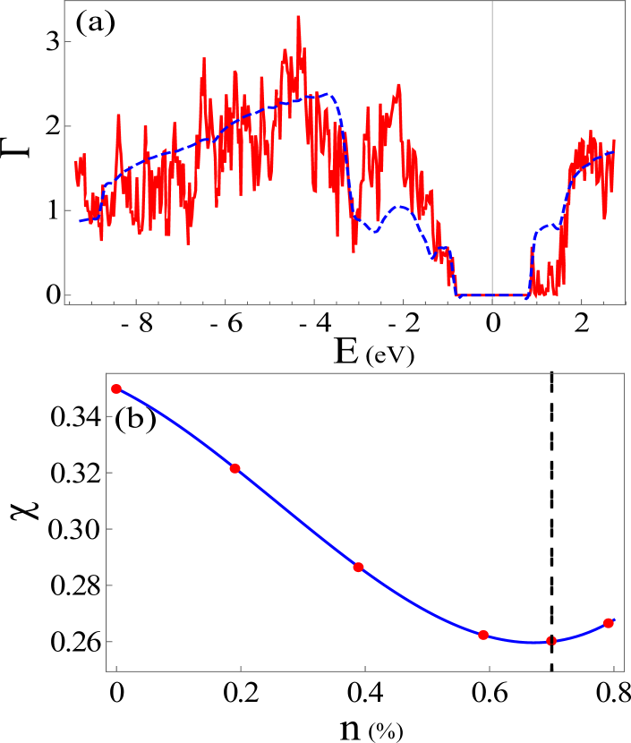
To show that this method is indeed model-independent we have also tested it in the case of a system fully described by Density Functional Theory (DFT). In particular, DFT-based conductance calculations were performed for armchair GNR of sizes unit cells and containing a specific spatial distribution of nitrogen atoms as substitutional impurities, which corresponds to . See SM [21] for details of the DFT calculations. The solid line in Fig. 4(a) shows the conductance spectrum of the system obtained within DFT, which will now serve as the input conductance for the inversion procedure. Regarding the CA conductance, there are two options on how can be obtained. First option is to repeat the steps taken to generate of Fig. 4(a) over several different disorder configurations. Bearing in mind that the impurity concentration must be kept as a variable parameter, the averaging procedure defined in Eq. (2) requires different configurations for every single value of , which indicates how computationally demanding this task might become if carried out entirely within DFT. The alternative option is to use the tight-binding (TB) model to carry out the CA calculation. In this case the TB model provides a fast averaging strategy without necessarily compromising in accuracy.
Here, we have selected the latter option and made use of DFT conductance spectra to identify suitable TB parameters that describe the nitrogen impurities in the GNR. See SM [21] for details, including a brief discussion on the choices available to extract TB parameters from DFT calculations [23, 24, 25, 26] and their implementation in large scale transport calculations [27, 28, 29]. The CA conductance is then generated within the TB model employing realizations, leading subsequently to the misfit function of Fig. 4(b). Once again, displays a minimum at exactly the same nitrogen concentration used to generated the input conductance . Another indication of success can be seen by plotting the CA conductance evaluated at the minimizing concentration of . Shown as a dashed line in Fig. 4(a), it has all the key features of even though both curves were calculated independently. Despite the computational complexity of obtaining the misfit function entirely within DFT, this has also been tested and, reassuringly, we find exactly the same answer (see SM [21] for details).
All input spectra in this manuscript were calculated from known Hamiltonians because it is then straightforward to test the success of the inversion method. Ultimately, inversions must be performed based on experimental conductance data of systems for which we do not have the full Hamiltonian. This calls for an inversion tool that is reliable, general and robust. The fact that our inversion strategy works for systems whose electronic structures are described by a simple TB model as well as by DFT calculations is indicative of the generality and robustness of this approach.
That disorder is beneficial to this inversion procedure is made evident by the distinction between the two panels of Fig. 2. Viewed at a fixed energy, the deviation between the input and the CA conductance spectra reveals very little about the system. In contrast, the misfit function entails a lot of information. The efficiency of the procedure relies on an ergodic hypothesis: conductance fluctuations of a single sample versus energy are related to sample to sample fluctuations at a fixed energy. More precisely, the ergodic hypothesis assumes that a running average over a continuous parameter upon which the conductance depends is equivalent to sampling different impurity configurations. Here the continuous parameter is the energy, but the concept can be extended to a range of other quantities, e.g., magnetic field, gate voltage, etc. A thorough mathematical discussion of this issue is beyond the scope of this manuscript, but it is worth mentioning that the ergodic hypothesis can be proven exactly for certain models of disordered systems[30, 31, 32]. That explains why the energy integration induces a distinctive minimum in since it is analogous to considering a wider universe of disorder configurations in the CA procedure. The success of the inversion procedure will therefore depend on how wide the integration range is. See SM [21] for details on the suitable choices for integration limits.
Another feature of the conductance fluctuations of quantum devices [7, 33] is that the correlation function is also universal [31]. The latter is characterized by a correlation length that is system dependent. Therefore, the method works best when the integration interval is such that . In our case, where we consider variations of the system chemical potential, scales with the mean level density times the transmission [34], which makes much larger than typical experimental temperatures, justifying our earlier claim that temperature has little effect on our inversion procedure. This also explains why the energy window used in the misfit-function definition does not have to be very large.
In summary, the inversion procedure presented here provides a mechanism capable of identifying the composition of scattering centres in a quantum device by simply looking at the energy dependence of the two-terminal device conductance. Assuming that the impurity type within the device is known, the procedure establishes the exact impurity concentration in it. Alternatively, if no information is known a priori about the scatterers, the inversion identifies their scattering strength and respective concentration. Finally, with a mixture of two different types of impurities we are able to establish the fractional concentration of each component of the device. Despite being presented with GNR, the technique is not material-specific and performs remarkably well in the ballistic, diffusive and at the onset of localised transport regimes. The method is based on the notion that conductance fluctuations carry little system-specific information, the average conductance depends smoothly on the variables of interest and on a standard ergodic hypothesis [30], requiring only an effective (single-particle) description of the system. 222 The applicability of the method for (strongly) interacting systems, i.e. beyond the mean field approximation, is not clear yet. This small set of conditions renders a very robust and versatile methodology that can extract structural and compositional information of quantum devices from standard transport measurements.
Acknowledgements.
The authors acknowledge support from FAPESP (Grant # FAPESP 2017/02317-2, 2016/01343-7, and 2017/10292-0), CNPq (Grants 308801/2015-6 and 312716/2018-4), FAPERJ (Grant E-26/202.882/2018), and the ICTP-Simons Foundation Associate Scheme. The authors also thank the National Laboratory for Scientific Computing (LNCC/MCTI, Brazil) for providing HPC resources of the SDumont supercomputer, which have contributed to the results reported here. Discussions with S. R. Power and M. Kucukbas are greatly acknowledged.References
- Datta [2005] S. Datta, Quantum Transport: Atom to Transistor (Cambridge University Press, 2005).
- Bertero and Piana [2006] M. Bertero and M. Piana, Inverse problems in biomedical imaging: modeling and methods of solution, in Complex Systems in Biomedicine, edited by A. Quarteroni, L. Formaggia, and A. Veneziani (Springer Milan, Milano, 2006) pp. 1–33.
- Virieux et al. [2017] J. Virieux, A. Asnaashari, R. Brossier, L. Metivier, A. Ribodetti, and W. Zhou, An introduction to full waveform inversion, in Encyclopedia of Exploration Geophysics (2017) p. 1.
- Tromp et al. [2008] J. Tromp, D. Komatitsch, and Q. Liu, Spectral-element and adjoint methods in seismology, Communications in Computational Physics 3, 1 (2008).
- Dias and Vieira Neto [2004] E. Dias and H. Vieira Neto, A novel approach to environment mapping using sonar sensors and inverse problems, in Lecture Notes in Computer Science, Vol. 9287, edited by C. Dixon and K. Tuyls (Springer, 2004).
- Lewenkopf and Weidenmüller [1991] C. H. Lewenkopf and H. A. Weidenmüller, Stochastic versus semiclassical approach to quantum chaotic scattering, Ann. Phys. 212, 53 (1991).
- Lee and Stone [1985] P. A. Lee and A. D. Stone, Universal conductance fluctuations in metals, Phys. Rev. Lett. 55, 1622 (1985).
- Tapasztó et al. [2008] L. Tapasztó, G. Dobrik, P. Lambin, and L. P. Biro, Tailoring the atomic structure of graphene nanoribbons by scanning tunnelling microscope lithography, Nat. Nanotechnol. 3, 397 (2008).
- Meir and Wingreen [1992] Y. Meir and N. S. Wingreen, Landauer formula for the current through an interacting electron region, Phys. Rev. Lett. 68, 2512 (1992).
- Datta [1995] S. Datta, Electronic Transport in Mesoscopic Systems (Cambridge University Press, Cambridge, 1995).
- Castro Neto et al. [2009] A. H. Castro Neto, F. Guinea, N. M. R. Peres, K. S. Novoselov, and A. K. Geim, The electronic properties of graphene, Rev. Mod. Phys. 81, 109 (2009).
- Das Sarma et al. [2011] S. Das Sarma, S. Adam, E. H. Hwang, and E. Rossi, Electronic transport in two-dimensional graphene, Rev. Mod. Phys. 83, 407 (2011).
- Lopez-Bezanilla and von Lilienfeld [2014] A. Lopez-Bezanilla and O. A. von Lilienfeld, Modeling electronic quantum transport with machine learning, Phys. Rev. B 89, 235411 (2014).
- Hansen et al. [2013] K. Hansen, G. Montavon, F. Biegler, S. Fazli, M. Rupp, M. Scheffler, O. A. Von Lilienfeld, A. Tkatchenko, and K.-R. Müller, Assessment and validation of machine learning methods for predicting molecular atomization energies, J. Theor. Comput. Chem. 9, 3404 (2013).
- Himmetoglu [2016] B. Himmetoglu, Tree based machine learning framework for predicting ground state energies of molecules, J. Chem. Phys. 145, 134101 (2016).
- Li et al. [2018] H. Li, C. Collins, M. Tanha, G. J. Gordon, and D. J. Yaron, A density functional tight binding layer for deep learning of chemical hamiltonians, J. Chem. Theory Comput. 14, 5764 (2018).
- Panosetti et al. [2019] C. Panosetti, A. Engelmann, L. Nemec, K. Reuter, and J. T. Margraf, Learning to use the force: Fitting repulsive potentials in density-functional tight-binding with gaussian process regression (2019).
- Xia and Kais [2018] R. Xia and S. Kais, Quantum machine learning for electronic structure calculations, Nat. Commun. 9, 4195 (2018).
- Dral [2020] P. O. Dral, Quantum chemistry in the age of machine learning, J. Phys. Chem. Lett. 11, 2336 (2020).
- Carrasquilla and Melko [2017] J. Carrasquilla and R. G. Melko, Machine learning phases of matter, Nat. Phys. 13, 431 (2017).
- [21] See Supplemental Material at [URL will be inserted by publisher] for more details.
- Note [1] An alternative definition of , shown in the SM [21], may extend the validity of the approximation to up to 7%.
- Gresch et al. [2017] D. Gresch, G. Autes, O. V. Yazyev, M. Troyer, D. Vanderbilt, B. A. Bernevig, and A. A. Soluyanov, Z2pack: Numerical implementation of hybrid wannier centers for identifying topological materials, Phys. Rev. B 95, 075146 (2017).
- Pizzi et al. [2020] G. Pizzi, V. Vitale, R. Arita, S. Blügel, F. Freimuth, G. Géranton, M. Gibertini, D. Gresch, C. Johnson, T. Koretsune, J. Ibañez-Azpiroz, H. Lee, J.-M. Lihm, D. Marchand, A. Marrazzo, Y. Mokrousov, J. I. Mustafa, Y. Nohara, Y. Nomura, L. Paulatto, S. Poncé, T. Ponweiser, J. Qiao, F. Thöle, S. S. Tsirkin, M. Wierzbowska, N. Marzari, D. Vanderbilt, I. Souza, A. A. Mostofi, and J. R. Yates, Wannier90 as a community code: new features and applications, J. Phys.: Condens. Matter 32, 165902 (2020).
- Nardelli et al. [2018] M. B. Nardelli, F. T. Cerasoli, M. Costa, S. Curtarolo, R. De Gennaro, M. Fornari, L. Liyanage, A. R. Supka, and H. Wang, PAOFLOW: A utility to construct and operate on ab initio hamiltonians from the projections of electronic wavefunctions on atomic orbital bases, including characterization of topological materials, Comput. Mater. Sci. 143, 462 (2018).
- Vanderbilt [2018] D. Vanderbilt, The pythtb package, in Berry Phases in Electronic Structure Theory: Electric Polarization, Orbital Magnetization and Topological Insulators (Cambridge University Press, 2018) pp. 327–362.
- Groth et al. [2014] C. W. Groth, M. Wimmer, A. R. Akhmerov, and X. Waintal, Kwant: a software package for quantum transport, New J. Phys. 16, 063065 (2014).
- Lima et al. [2018] L. Lima, A. Dusko, and C. Lewenkopf, Efficient method for computing the electronic transport properties of a multiterminal system, Phys. Rev. B 97, 165405 (2018).
- João et al. [2020] S. M. João, M. Anđelković, L. Covaci, T. G. Rappoport, J. M. Lopes, and A. Ferreira, Kite: high-performance accurate modelling of electronic structure and response functions of large molecules, disordered crystals and heterostructures, R. Soc. Open Sci. 7, 191809 (2020).
- French et al. [1978] J. French, P. Mello, and A. Pandey, Ergodic behavior in the statistical theory of nuclear reactions, Phys. Lett. B 80, 17 (1978).
- Brézin and Zee [1994] E. Brézin and A. Zee, Correlation functions in disordered systems, Phys. Rev. E 49, 2588 (1994).
- Guhr et al. [1998] T. Guhr, A. Müller-Groeling, and H. A. Weidenmüller, Random-matrix theories in quantum physics: common concepts, Phys. Rep. 299, 189 (1998).
- Lee et al. [1987] P. A. Lee, A. D. Stone, and H. Fukuyama, Universal conductance fluctuations in metals: Effects of finite temperature, interactions, and magnetic field, Phys. Rev. B 35, 1039 (1987).
- Alves and Lewenkopf [2002] E. R. P. Alves and C. H. Lewenkopf, Conductance fluctuations and weak localization in chaotic quantum dots, Phys. Rev. Lett. 88, 256805 (2002).
- Note [2] The applicability of the method for (strongly) interacting systems, i.e. beyond the mean field approximation, is not clear yet.