Characterization of single photon sources for radiometry applications at room temperature
Abstract
A single photon source with high repeatability and low uncertainties is the key element for few-photon metrology based on photon numbers. While low photon number fluctuations and high repeatability are important figures for qualification as a standard light source, these characteristics are limited in single photon emitters by some malicious phenomena like blinking or internal relaxations to varying degrees in different materials. This study seeks to characterize photon number fluctuations and repeatability for radiometry applications at room temperature. For generality in this study, we collected photon statistics data with various single photon emitters of at low excitation power and room temperature in three material platforms: silicon vacancy in diamond, defects in GaN, and vacancy in hBN. We found common factors related with the relaxation times of the internal states that indirectly affect photon number stability. We observed a high stability of photon number with defects in GaN due to faster relaxations compared with vacancies in hBN, which on the other hand produced high rates () of photons per second. Finally, we demonstrate repeatable radiant flux measurements of a bright hBN single photon emitter for a wide radiant flux range from a few tens of femtowatts to one picowatt.
Keywords: single photon emitters, quantum radiometry, photon number metrology
1 Introduction
Advances in photon measurements have stimulated innovation in encrypted communications and information processing, distinguished by a single datum being encoded in a single photon [1, 2]. As relevant techniques mature, accuracy in photon generation and detection is growing to compete with the present standard of radiative flux. A new standard is thus being defined by photon flux, in which counting is a central element for information processing with photons, and which is differentiated from the present standard where absoluteness is given by foreign physical systems based on electrical current and temperature [3, 4, 5, 6].
For the realization of this new standard, the accurate calibration of photon flux as well as high-purity single photon generation are prerequisite [7]. Commonly used single photon counters like avalanche diodes and superconducting nanowires have a short period of breakdown after a detection event [8, 9], and require post-corrections to represent real radiant flux with pre-assumptions about photon statistics. Recent correction techniques supposing a Poisson distribution have achieved repeatable accuracies with parameters of quantum efficiency and detection dead time, promising that the counting-based standard can soon compete [10]. To improve even further, the goal has become achieving single photon generation that deterministically furnishes a single photon only when the detector is ready to count, or at least with a certain and uniform probability [11, 12, 13].
Such an ideal source has to maintain single photon flux with low fluctuations and high repeatability. Current sources, however, show complex behaviors of relaxations, and as a result their emission blinks [14, 15]. In this study, we focus on materials that emit single photon fluorescence at room temperature by investigating silicon vacancy in diamond, defects in GaN, and vacancy in hBN as spectrally narrow and accessible platforms. We characterize photon number statistics and fluctuations since their degrees are the major factors in determining the accuracy of photon flux for radiometry applications. Additionally, we compare the maximum count rate allowed for the bare materials under the conventional collection technique of confocal microscopy. The reason why we stress this condition is that detection count rates are not intrinsic but rather depend on efficiencies given by refractive index geometries and detection techniques. We note that the present experiments are limited by estimations of internal quantum efficiency and the theoretically maximum count rates under continuous wave operation; more specific methods to optimize collection efficiency, an important subject of photonics, remain for future, application-oriented studies.
To find general tendencies and characteristics from among the complexity and variety of our materials, the current work was based on a large amount of data collected from numerous emitters. Our full dataset consists of two levels: the first concerns basic properties in identifying single photon emitters, and the second concerns figures of stability. Data fields in the first level are of photon coincidence correlation and spectra, which have been used to authenticate single photon fluorescence. Statistical distributions of the positions of the spectral peaks were collected as a subject for later studies on defect states and their formations. We discuss the results of these basic properties in section 3.
Data fields in the second level include photon number uncertainty and the repeatability of measurements for conversion to radiometry flux. They are examined with a dual detection system that measures photon streams with two modes of detection, namely, photon counting detectors with results in count per second (cps) and photocurrent-generating photodiodes with results in joules per second (W). Having two different detection mechanisms enables a comparison of outcomes for the same single photon stream as well as an examination of the uncertainty of conversion between the two measures. Setting the system to photon counting detectors, we measured both photon number fluctuation and repeatability of photon flux measurements to evaluate the degrees of stability both for the photon sources and for the detection system itself, respectively. Analyzed results are discussed in sections 4–5.
The main difficulty in radiant flux measurements is to find an emitter that produces a photon flux intense enough to be detected by the photocurrents of the photodiode. To this end, we exploited an emitter of count rate per second and . We verified both the repeatability of measurement of the radiant flux generated by the single photon emitters and the equivalence of the calibration parameters of detection, as described in section 5. We did not find additional corrections other than our given parameters [10], which was expected from our collection efficiency of that flattens any dissimilar photon number statistics into Poisson distribution [16]. Increasing collection efficiency will be our main subject in future studies to achieve the advantages of sub-Poisson statistics, which is being pursued for few-photon metrology.
2 Samples and Experimental Methods
Materials of interest are silicon vacancy in diamond (vc-SiV), crystal defects in GaN (df-GaN), and vacancy in hBN (vc-hBN). Their common feature is a wide band-gap of the host crystal that preserves single photon emission at room temperature. The SiV sample in this work took the form of nano-diamonds on an iridium substrate, which were grown to the shape of the film by the silicon-free CVD process and milled to diameters of 50–100 nm. Silicon was implanted after the clean CVD process to attain a high SiV purity [17]. The GaN substrates are a commercially available 4 m GaN crystal grown on sapphire [18]. The fluorescence center in GaN was explained to be a charge-trapped dot that locates at the intersection of a lattice dislocation stemming from the sapphire–GaN interface and a layer mismatch of crystal orientation, similar to the point-like potential wall in a two-dimensional quantum well [14]. The hBN sample took the form of nano-flakes dispersed on an oxidized layer of silicon substrate. The nano-flakes are commercially available, but required a special treatment of annealing in an inert environment: 800∘C for 30 min in 1 Torr Ar gas [19].
Because emitters are randomly distributed, confocal microscopy has been commonly used to confine fluorescence signals. We were helped by the measurement system of our previous work, where we set up modules of single photon collection with single mode fibers (SMFs) and analyzed their photon number statistics [20]. The setup has benefits of uninterrupted serial measurements of spatial positions, spectra and photon statistics (), and a high stability of maintained alignments that leads to repeatable measurements (see section 5). The SMF interface gives identical beam profiles for analyzing the modules, leaving the external systems available for exploitation. The theoretically maximum collection efficiency from the sample–air interface to the SMF output is 21 %, assuming a Gaussian beam as in past work [20]. The collection efficiency % was drawn with consideration of the mode coupling efficiency of an electrical dipole radiation and a SMF mode.[21, 22] (For more details, see A.) The real collection efficiency is smaller than this prediction though when we take into account surface scattering and all the variable nano-crystal shapes. Still, our photon count rate results are similar to other works that studied the same materials, implying a sufficient level of mechanical rigidity to maintain the count rate.
For the evaluation of photon number fluctuation and application to radiometry experiments, we constructed a radiometry module that includes the dual detection system described above. This new module has two stages of detection: the first is counting photon flux with a silicon single photon avalanche detector (SPAD), and the second is measuring radiant power converted from the photodiode photocurrents. They share the same single photon input injected via SMF, and the same incidence position at which we rotate groups of detectors to place. This intends to attain convergence between the outcomes of the two detection mechanisms consistently without any corrections for optical path loss (section 5). The module also helped the measurement of photon number fluctuations, as shown in section 4.
3 Spectra and Photon Statistics
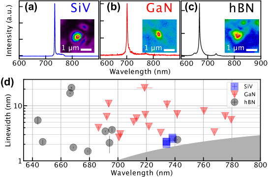
Spectra of fluorescence centers commonly consist of a zero-phonon line (ZPL) and phonon side-bands, and show a high ratio of ZPL intensity compared to the photon side-band, i.e., a high Debye–Waller factor, as shown in figure 1(a–c). The ZPL positions of vc-hBN and df-GaN depend on strain and defect formations, and are widely distributed over 600–750 nm and 690–800 nm, respectively [figure 1(d)]. Due to the different mechanisms of defect formation between df-GaN and vc-hBN, df-GaN has a greater linewidth on average and can be more directly affected by crystal strain. Likewise, both df-GaN and vc-hBN have a wider linewidth on average, which can vary by the local strain of the host crystal because of the various kinds of defect formations and their large degrees of freedom. On the other hand, vc-SiV has a definite ZPL position, nm[23], the formation of which is explicitly allowed by the diamond crystal.

For a statistical approach, we collected photon statistics from 20 fluorescence emitters. Single photon emitters have a unique property of fluorescence, exhibiting a low coincidence of photon count. The degree and time scale of this coincidence suppression have been commonly represented by a normalized correlation () of photon count () as measured by a Hanbury Brown–Twiss interferometer (HBT) [16]. We employed two methods of deducing experimentally: start-stop histogram and time-tag correlation (TTC). The former is advantageous for real-time acquisition as the trigger intervals between signals from two SPADs are collected. The latter though has a better convergence at because this method stores time-tags crudely and deduces a normalization factor from the total count of each detector during data processing, which gives reliable results of . In our study, estimations of were based on raw data given by the TTC method.
The from our samples, however, shows composite features of both anti-bunching () at and bunching () at simultaneously. Here, and are effective time constants defined by the fitting model , where is the depth contributing to the anti-bunching of , is the height above , is the time width of anti-bunching, and is the characteristic exponential decay time of bunching. We collected and because they have physical origins: is the spontaneous emission time for an ideal photon source or relates to the lifetime of the radiative transition for single photon emission, while stems from non-radiative relaxations, which can cause blinking in the photon emission.[24] If a single emitter is trapped in meta-stable dark states, it stops emitting until it is released to bright states, with directly representing this time scale.
With this model, we observed for vc-SiV, for df-GaN, and for vc-hBN, as shown in figure 2(a–c), where the errors are the widths of the 95 % confidence interval calculated via robust covariance estimation [25]. The full data was measured from 20 fluorescence centers of our samples as shown in figure 2(d). The large errors in the obtained from SiV emitters are due to the short of these emitters and a time jitter of the detector. To restore the pure before time jitter noises, we tried a deconvolution method with a noise filter assumed for a time jitter ns.[26] Our method of deconvolution is to fit data with a convolution form of exponential function. However, this method is redundant as its results are similar to the previous estimation of with parameters of and , and they can be biased when is overestimated. It is a common tendency regardless of materials that time jitter errors of grows as is shortened. Since measured by TTC is in absolute values, we could take the average for some intervals of . These experimentally allowed values are also presented as transparent points from 18/hBN fluorescence emitter shown in figure 2(d). Their differences from pure values of the model are reflected in confidence intervals for all emitters.
Our closest recorded values to 0 were attained around from df-GaN and from vc-hBN, both of which are allowed at a low excitation power. The effective excitation power differed among materials and samples due to the differences in refractive index, diameter of grains, and geometry. However, the set of data used for figure 2(d–f) comprises the full range of photon count rates achieved from far below and above the saturation points of each material. We suspect that the lowest value of can either be attributed to background photoluminescence, including deeper infrared, as we used a long pass filter with a 568 nm edge for purification, or the unresolved single photon emitting transitions in a ZPL [27]. We discuss this in section 5 with figure 6.
Our result shows that and decrease with an increasing excitation power for every material we observed. These variables of the model has an origin in relaxation processes of fluorescence materials. The power dependence of evidently shown with df-GaN and vc-hBN implies that represents a re-excitation rate rather than a spontaneous emission rate under moderate that allows exploitable photon count rates. Nevertheless, we can expect large spontaneous emission rates from SiV, whose is as short as being close to the instrumental limit of time jitter at the entire range of . According to the three level model, are related to a recovering relaxation from meta-stable states (deshelving), and also depends on excitation power because it gives more chances of initializing ionization [24, 14, 28].
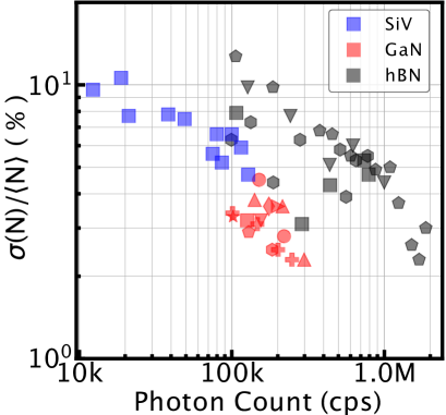
We observed high count rates of cps with vc-hBN, similar to other studies [29], and low count rates of cps with vc-SiV. This result is opposed to the long of hBN, as shown in figure 2(e) and (f), and to the intuition that fast transitions allow high photon rates. The speed of the transitions and blinking of vc-SiV was the highest among the materials of interest, but exact pictures of these have yet to be unveiled to predict the internal efficiency of fluorescence emissions at room temperature [30, 31]. The photon count rate of df-GaN, cps, seems limited by total internal reflections at the GaN–air interface, which can be overcome by an immersion medium before the objective lens. Otherwise, vc-hBN is preferable for radiometry experiments that require a wide range of photon counts on the order of cps.
4 Photon number fluctuation
Low photon number uncertainty is required for an ideal photon source. From various values of depending on the emitters and materials, which are related to the time scales of emission blinking, we can infer the requirement to find one that has a low photon number fluctuation. We first measured the photon number uncertainty (), defined as the ratio of the standard deviation of photon number () to its average value (). These statistical variables were obtained by a single shot of streaming acquisition of photon counts over 10 s. Photon number is the accumulated photon count in a 10 ms long time bin () within the streaming acquisition. Thus, we clarify the terminological distinction between and photon count rate by the following relation:
| (1) |
for an -th time bin . In experiments, we measured directly from an edge counter with a fixed and then deduced via .
For shot-noise limited in Poisson statistics as acquired for , the defined photon number uncertainty can be reduced to , which tends to decrease with increasing . This assumption excludes the observed differences of uncertainty between the materials shown in figure 3(a). Measured values of the uncertainty are split into two groups: SiV with GaN, and hBN on the other side. With a few exceptions, every hBN emitter exhibited a larger than SiV and GaN.
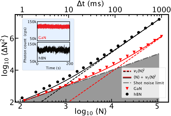
Additional noises other than the shot-noise are clearly seen. We examined with integration times () from 1 ms to 1 s for df-GaN and vc-hBN; was set to a similar value ( cps) by adjusting excitation power. In this condition, for the df-GaN and for the vc-hBN, with both emitters below saturation. We extrapolated the noise model to include the quadratic term of with the coefficient :
| (2) |
This model was fitted to df-GaN with , and as shown in figure 4, was close to at 20 ms and small . However, the data from vc-hBN was close to the model only for large with , and did not converge to at short . The of vc-hBN was greater than that of df-GaN by an order of magnitude, as much as the difference of between them.
The large fluctuation of in vc-hBN can easily be seen from the real-time data in the inset of figure 4. The origin is related with the blinking phenomenon, as vc-hBN has long s. This value is in contrast to the short ns of df-GaN. In our survey of 36 fluorescence centers, most vc-hBN , which are related to the time dynamics of the blinking, are slower than those of GaN, as shown in figure 2(f). This analysis of is still insufficient to extrapolate the general blinking dynamics though, since we could not measure ms in due to the sampling time window. Nevertheless, this tendency of slow blinking dynamics being more clearly seen in vc-hBN, as shown in the inset of figure 4, is intriguing. On the other hand, df-GaN with the fast did not exhibit such fluctuations, and enabled the low noise with ms.
Because of the low of vc-SiV, we could not perform a fair test of for the vc-SiV samples. However, the analogous behavior of with df-GaN as shown in figure 4 leads us to expect that of vc-SiV would be as low as that of df-GaN if it had a similar level of . The low of vc-SiV also has disadvantages in obtaining repeatable , as in the following section.
5 Conversion Between Photon and Radiant Fluxes with High Repeatability
In order to apply single photon emitters in radiometry experiments, evaluations of reliability in measurement results must precede. The main quality of our assessment is the repeatability of photon flux () or photon count () measurement followed by conversion to radiant flux (). We performed two tests: one to deduce the repeatability errors of , and the other to confirm the validity of applying present calibration parameters for photon counts to represent radiant fluxes. The dual detection module introduced in section 2 is well suited for performing these tests. With this module, we measured and from a SPAD and photodiode, respectively, and cross-checked the independent results with previously proven calibration parameters.
Repeatability errors were measured via the following process. We repeated the streaming acquisition of the same as we did for photon number uncertainty in section 4. We took the average value () of each shot () and repeated times to obtain , thereby yielding the repeatability error as according to its theoretical definition. In order to obtain practical values, we inserted an measurement process between each shot of acquisition to mirror the calibration sequence in radiometry experiments. Hence, we attain results of both repeatability error and data on and .
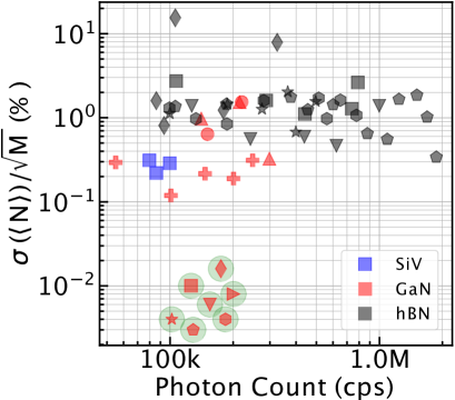
As shown in figure 5, df-GaN, which has low , demonstrates a high repeatability of measurement. We extended to 20 to obtain the upper bound of repeatability with a qualified df-GaN emitter with and cps. This highest result reaches to 30 ppm, as marked with green circles in figure 5. We note that this value is close to the present repeatability of radiometry experiments with this laser source.
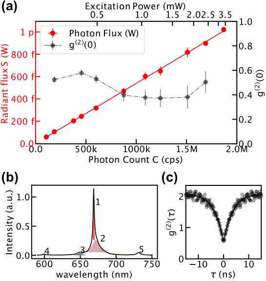
Despite a low fluctuation and high repeatability, the maximum obtained from df-GaN has a lower limit around cps [figure 2(d–f)]. This also limits the signal to noise ratio (SNR) to 22 for measurements by a silicon photodiode having a noise equivalent power (NEP) of 8.4 fW/ and integrating photocurrents for 10 s [32, 33]. To take advantage of the high SNR of and the wide range of flux levels shown in figure 6, we chose 18/hBN among vc-hBN emitters (see figure 2), whose maximum cps. We adjusted the level of by controlling the excitation power (). has a behavior following the function with a saturation count rate of cps and a saturation power of mW. Over this wide range of , remained within the range 0.37–0.58. The uncertainty of (confidence interval 95 % trust) increased at high , as strong excitation power shortens the anti-bunching time width into the time jitter limit of SPAD, as shown in figure 2(e).
As shown in figure 6(c), when measured at a low excitation power of , and it decreases to 0.35 at higher . We attribute this irregularity to the presence of other transitions that independently emit single photons. Spectral investigations reveal that the ZPL is composed of two Lorentzian peaks, labeled 1 and 2 in figure 6(b). Similar findings were observed in another work, and according to the previous analysis we can predict that cross-correlations between independently emitted single photons increase [27]. As the overlapped peaks 1 and 2 have mostly similar areas, the degree of mixture is sufficient to be the main cause of the high . We also attribute the oscillating behavior of with respect to to a property of mixture in which different excitation cross-sections of fluorescence transitions make them compete in contributing to a sum of photon count rate.
Thanks to the narrow linewidth ( nm) shown in figure 6(b), we took a single value of at the center wavelength nm [10], with the justification that at the within the narrow line is smaller than the measured uncertainty (0.5 %). Error caused by detection dead time and nonlinear counting was predicted to be 0.2 % at cps and grow to 4 % at cps, so that error correction is critical for cps. For this, we used the correction function to present the corrected count rate , as defined in a previous work [10]. At this stage, with given quantum efficiency , we can extract the important . In practice, we can reduce this to by introducing an effective function that includes both effects of and [10]. Then we represent the relation between and in a convenient form with the uncorrected variable :
| (3) |
This relation with given agrees well with the experimental and data shown in figure 6(a). We first note that the parameters given in previous works were applied here identically, even though the measurement system in this work was newly fashioned. Second, identical results were achieved even with a non-classical light source that was not fully controlled, as this new source contained uncontrolled internal dynamics related to and the blinking phenomenon. Such a photon source may reduce the repeatability of due to a high , but it does not cause contradictions with the given parameters in because the parameters are central values.
6 Discussions
We have studied single photon emitters based on fluorescence defects in various crystal materials at room temperature. Silicon vacancy in diamond, defects in GaN, and vacancy in hBN platforms all have a narrow linewidth, and their spectrum centers are spread over a wide range of wavelengths. This is, in fact, an important advantage for few-photon radiometry where we have various quantum efficiencies as variable parameters in conversion models for radiant power.
Both stability and brightness are important qualities of single photon sources in few-photon metrology. None of the materials investigated in this study are endowed with both characteristics simultaneously. For example, although single photon sources in hBN nano-flakes exhibit high rates of photon detection, they are interrupted by slow blinking, which causes severe fluctuations in photon count rates. On the other hand, those in GaN show a high degree of stability and a high repeatability of emission rate, while their photon count rates are lower than those attained from hBN.
Such differences can be expected from their shapes. Emitters in hBN are close to the surface or edges in a nano-flake, where electrostatic fields can have large effects and cause vulnerability to charge fluctuations. The scenario of severe blinking in hBN is also supported by a recent study that revealed many internal states and frequent relaxations between them, even at low temperature. On the other hand, emitters in GaN are embedded at a depth of a few micrometers, and this reduces the fluctuations caused by electrostatic fields. However, the flat surface with high refractive index of GaN significantly decreases its photon collection efficiency, according to the total internal reflection effect [34].
Various methods have been developed to alleviate total internal reflection. This has long been a subject to mitigate the surface effects in solar cells and light-emitting diodes, and many techniques have been developed. The simplest solution is a solid immersion lens that includes various lens techniques like micro-half spheres and meta-surfaces. These methods do not modify the regions near the emitters beneath the surface. We are expecting high collection efficiencies as supported by these methods, which will enable us to apply non-classical photon number statistics, like one corresponding to the Fock state, and to achieve a high degree of number uncertainty.
Appendix A Coupling efficiency of radiation from a point dipole source to a single mode optical fiber
We assume an electric dipole source laid at a focal point in air and perpendicular to cylindrical symmetry axis connecting an objective lens and a single mode fiber (SMF) collimation lens. Electromagnetic fields that refocused by the SMF collimation lens were analytically calculated from the Green dyadic function, while the radio of field intensity collected through a finite numerical aperture 0.95 () was extracted [21]. Because the refocused field has a different profile from a SMF mode, a field-to-field coupling efficiency () is calculated using an inner product defined in [22]. Then, . Considering a setup loss , the overall efficiency excluding unknown substrate losses is reduced to .
Acknowledgments
This work was partially funded by National Research Council of Science and Technology (NST) of the Republic of Korea (CAP-15-08-KRISS) and Korea Research Institute of Standards and Science (KRISS) (KRISS-2019-GP2019-0020). The authors declare no conflicts of interest.
References
References
- [1] Tittel W and Weihs G 2001 Quantum Info. Comput. 1 3–56
- [2] Chen S, Chen Y A, Strassel T, Yuan Z S, Zhao B, Schmiedmayer J and Pan J W 2006 Phys. Rev. Lett. 97(17) 173004
- [3] Willson R C 1973 Appl. Opt. 12 810
- [4] Martin J E, Fox N P and Key P J 1985 Metrologia 21 147
- [5] Cheung J Y, Chunnilall C J, Woolliams E R, Fox N P, Mountford J R, Wang J and Thomas P J 2007 J. Mod. Opt 54 373
- [6] Zwinkels J C, Ikonen E, Fox N P, Ulm G and Rastello M L 2010 Metrologia 47 R15
- [7] Chunnilall C J, Degiovanni I P, Kück S, Müller I and Sinclair A G 2014 Optical Engineering 53 1
- [8] Cova S, Ghioni M, Lacaita A, Samori C and Zappa F 1996 Appl. Opt. 35 1956
- [9] Kerman A J, Dauler E A, Keicher W E, Yang J K W, Berggren K K, Gol’tsman G and Voronov B 2006 Appl. Phys. Lett. 88 111116
- [10] Bae I H, Park S, Hong K S, Park H S, Lee H J, Moon H S, Borbely J S and Lee D H 2019 Metrologia 56 035003
- [11] Rodiek B, Lopez M, Hofer H, Porrovecchio G, Smid M, Chu X L, Gotzinger S, Sandoghdar V, Lindner S, Becher C and Kuck S 2017 Optica 4 71
- [12] Vaigu A, Porrovecchio G, Chu X L, Lindner S, Smid M, Manninen A, Becher C, Sandoghdar V, Götzinger S and Ikonen E 2017 Metrologia 54 218
- [13] Lombardi P, Trapuzzano M, Colautti M, Margheri G, Degiovanni I P, López M, Kück S and Toninelli C 2020 Adv. Quantum Technol. 3 1900083
- [14] Berhane A M, Jeong K Y, Bodrog Z, Fiedler S, Schröder T, Triviño N V, Palacios T, Gali A, Toth M, Englund D and Aharonovich I 2017 Adv. Mater. 29 1605092
- [15] Konthasinghe K, Chakraborty C, Mathur N, Qiu L, Mukherjee A, Fuchs G D and Vamivakas A N 2019 Optica 6 542
- [16] Loudon R 1973 The Quantum Theory of Light (Oxford: Clarendon Press)
- [17] Neu E, Steinmetz D, Riedrich-Möller J, Gsell S, Fischer M, Schreck M and Becher C 2011 New J. Phys 13 025012
- [18] The film (2-m p-type/2-m undoped) grown on sapphire, supplied by Suzhou Nanowin Science and Technology Co., Ltd..
- [19] Tran T T, Elbadawi C, Totonjian D, Lobo C J, Grosso G, Moon H, Englund D R, Ford M J, Aharonovich I and Toth M 2016 ACS Nano 10 7331
- [20] Lim H J, Jeong K Y, Lee D H and Hong K S 2019 Opt. Mater. Express 9 4644
- [21] Novotny L and Hecht B 2012 Principles of Nano-Optics (Cambridge University Press) chap 3 2nd ed
- [22] Schneider P I, Srocka N, Rodt S, Zschiedrich L, Reitzenstein S and Burger S 2018 Opt. Express 26 8479
- [23] Goss J P, Jones R, Breuer S J, Briddon P R and Öberg S 1996 Phys. Rev. Lett. 77(14) 3041
- [24] Santori C, Fattal D, Vučković J, Solomon G S, Waks E and Yamamoto Y 2004 Phys. Rev. B 69 205324
- [25] Sidik K and Jonkman J N 2016 Statistics in Medicine 35 4856
- [26] Nomura M, Kumagai N, Iwamoto S, Ota Y and Arakawa Y 2010 Nat. Phys. 6 279
- [27] Alexander B and Christoph B 2019 Nanophotonics 8 2041
- [28] Astakhov G V and Dyakonov V 2018 Defects for quantum information processing in sic Defects in Advanced Electronic Materials and Novel Low Dimensional Structures ed Stehr J, Buyanova I and Chen W (Woodhead Publishing) p 211
- [29] Nguyen M, Kim S, Tran T T, Xu Z Q, Kianinia M, Toth M and Aharonovich I 2018 Nanoscale 10(5) 2267
- [30] Neu E, Arend C, Gross E, Guldner F, Hepp C, Steinmetz D, Zscherpel E, Ghodbane S, Sternschulte H, Steinmüller-Nethl D, Liang Y, Krueger A and Becher C 2011 Appl. Phys. Lett. 98 243107
- [31] Lindner S, Bommer A, Muzha A, Krueger A, Gines L, Mandal S, Williams O, Londero E, Gali A and Becher C 2018 New J. Phys 20 115002
- [32] Mountford J, Porrovecchio G, Smid M and Smid R 2008 Appl. Opt. 47 5821
- [33] Park S, Hong K S and Kim W S 2016 Appl. Opt. 55 2285
- [34] Bowman S R, Brown C G, Brindza M, Beadie G, Hite J K, Freitas J A, Eddy C R, Meyer J R and Vurgaftman I 2014 Opt. Mater. Express 4 1287