Radiative properties of quantum emitters in boron nitride from excited state calculations and Bayesian analysis
Abstract
Point defects in hexagonal boron nitride (hBN) have attracted growing attention as bright single-photon emitters. However, understanding of their atomic structure and radiative properties remains incomplete. Here we study the excited states and radiative lifetimes of over 20 native defects and carbon or oxygen impurities in hBN using ab initio density functional theory and GW plus Bethe-Salpeter equation calculations, generating a large data set of their emission energy, polarization and lifetime. We find a wide variability across quantum emitters, with exciton energies ranging from 0.3 to 4 eV and radiative lifetimes from ns to ms for different defect structures. Through a Bayesian statistical analysis, we identify various high-likelihood defect emitters, among which the native defect is predicted to possess emission energy and radiative lifetime in agreement with experiments. Our work advances the microscopic understanding of hBN single-photon emitters and introduces a computational framework to characterize and identify quantum emitters in 2D materials.
Introduction
Two-dimensional (2D) materials are rapidly becoming a new platform for photon based quantum information technologies 1, 2.
The discovery of single-photon emitters (SPEs) at point defects in hBN 3 has spurred an intense search for optically active defects in 2D crystals 4.
Compared to defects in bulk crystals, such as diamond and silicon carbide 5, 6, 7, 8,
defects embedded in 2D materials promise to be more easily addressed and controlled.
In the case of hBN, defect emitters exhibit a range of desirable properties, including high emission rate, room temperature stability, strong zero-phonon line (ZPL) and easy integration with other optical components using 2D hBN crystals 1, 9, 10, 11, 12.
A pressing challenge for defect emitters in hBN is identifying their atomic structure. Various possible structures have been proposed on the basis of density functional theory (DFT) calculations
and their comparison with experiments 3, 13, 14, 15, 16, 17, 18, 19.
However, while DFT can provide valuable insight into the formation energy, symmetry and electronic structure of SPE defects,
it cannot address key aspects of point-defect SPEs such as their excited states and radiative processes responsible for light emission.
To complicate the matter further, similar to other 2D materials and their defects 20, 21, 22,
optical transitions at defects in hBN are dominated by excitonic effects 23, which require specialized first-principles calculations beyond the scope of DFT. Quantum chemistry approaches and density matrix renormalization group have also been used to investigate specific defect structures 24, 25, but wide comparisons among different structures are still missing.
The Bethe-Salpeter equation (BSE) can accurately predict optical properties and excitons in materials 26.
It also enables, due to recent advances, precise calculations of radiative lifetimes in 2D and bulk crystals 27, 28, 29, 30.
The radiative lifetime plays an important role in the study of SPEs as it determines the shortest decay time constant in the second-order photon correlation function 31, 32 and can also be measured directly from fluorescence intensity decay 3, 10.
Applying the BSE and related methods to defect emitters in hBN would enable direct comparisons between theory and experiment of the emission energy and radiative lifetime, providing valuable information to identify defect SPEs.
Yet, first-principles BSE calculations are computationally costly to carry out on defect structures,
and the radiative lifetime calculations are only a recent development.
In this work, we employ the BSE approach to compute from first principles the optical properties, transition dipoles, excitons and radiative lifetimes of atomic defects in hBN.
We examine a large pool of candidate SPE structures, spanning native defects and carbon or oxygen impurities, to correlate their atomic structures with their photophysics.
We find that different quantum emitters exhibit radiative lifetimes spanning six orders of magnitude and emission energies from infrared to ultraviolet.
Bayesian statistical analysis is employed to correlate our results with experiments and identify the most likely SPEs in hBN, among which we find the defect to have the highest likelihood.
In-depth calculations on the defect highlight the strong dependence of its radiative properties on small perturbations to its atomic structure.
The dependence of the defect radiative properties on dielectric screening is analyzed by comparing monolayer and bulk hBN results.
Our systematic investigation addresses key challenges for characterizing the excited states and radiative properties of defect emitters in 2D materials.
Results
Our candidate defect structures consist of charge-neutral native defects and carbon or oxygen impurities occupying one or two atomic sites, for a total of 8 different native defects and 7 structures for each of carbon and oxygen impurities.
We compute the ground state defect properties using DFT, employing fully relaxed defect atomic structures in 55 supercells of monolayer hBN (and for some defects, in bulk hBN).
We then refine the electronic structure of selected defects using GW calculations 33, followed by BSE calculations to obtain the exciton energies and wave functions and from them the optical absorption, transition dipoles and radiative lifetimes (see the Methods section).
In the following, we denote the defects in hBN as if neighboring N and B atoms are replaced by species X and Y, respectively, where X and Y can be a vacancy or another element 13, 3.
We focus on emitters in the interior of the 2D crystal 34, 35 and do not consider defects that would likely appear at the sample edges or corners 36, 37.
The electronic energies obtained using DFT, while in general not representative of electronic or optical transitions, can be used for guidance and for estimating qualitative trends.
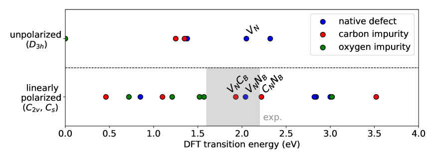
Figure 1 shows the lowest spin-conserving transition (HOMO-LUMO) energy of the candidate defects, obtained from DFT,
together with the emission polarization inferred from structural symmetry. The defect structures considered here exhibit three different types of local symmetries, , , and .
In the high symmetry structure, adopted by , , , , , , emitted light cannot be linearly polarized.
Conversely, linearly polarized emitted light, as observed experimentally in hBN SPEs 11, is possible in the and symmetries.
In the configuration, which is the most common among the defects investigated here, the 3-fold rotational symmetry is broken but all the atoms remain in-plane, preserving the mirror symmetry with respect to the crystal plane.
The symmetry found in the , , and defects is instead associated with an out-of-plane distortion that breaks the mirror symmetry about the plane.
The DFT transition energies for the 22 defect structures range from 0 to 3.5 eV. In contrast, the ZPL of the measured SPEs are in the 1.62.2 eV energy range 11, as shown by the shaded region in Fig. 1.
While candidate structures with symmetry can be ruled out, and structures with exceedingly small or large DFT transition energies also appear unlikely on the basis of the DFT results.
Starting from the DFT ground state, for selected defects we compute the excited state properties with the GW-BSE method, obtaining the quasiparticle energies in the one-shot approximation and the exciton energies and wave functions with the BSE, which captures electron-hole interaction and excitonic effects. We combine the solutions of the BSE with an approach we recently developed 29, 30 to compute the radiative lifetime of an exciton state from Fermi’s golden rule. Generalizing our previous formula for isolated (0D) emitters 29 to include anisotropic dielectric screening in hBN, the radiative decay rate (inverse of radiative lifetime) of an exciton state is:
| (1) |
where and are the in-plane and out-of-plane dielectric function of hBN, respectively, is the in-plane photon wavevector, is the exciton energy and and are the corresponding components of the exciton transition dipole.
We use a constant in-plane dielectric function for bulk hBN () at optical wavelengths, and for monolayer hBN we take into account the dependence on wavevector as
38, where is a constant equal to 0.4 nm 39.
In this approach, which is appropriate for 2D materials, the in-plane dielectric function of monolayer hBN reduces to a value of 1 when the wavevector equals the wavevector of a photon at optical frequencies.
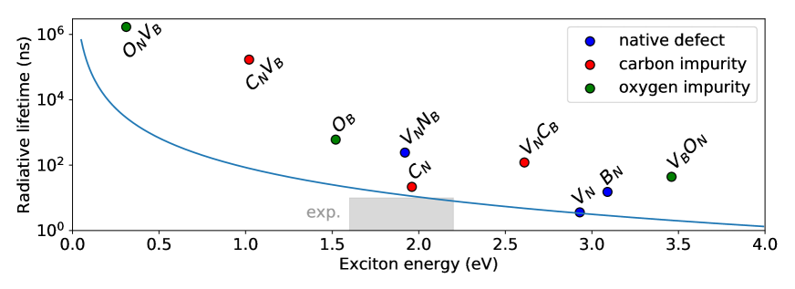
Figure 2 shows the computed radiative lifetimes and lowest bright exciton energies for nine selected defects, including , , , , , ,
, and . We find that the exciton energy can differ significantly by as much as 1 eV from the corresponding DFT transition energy, which fails to account for screening and electron-hole interaction effects.
This result is a testament to the importance of excited state calculations for investigating SPEs.
Surprisingly, we find that the computed radiative lifetime for the selected structures span six orders of magnitude, from about 1 to 106 ns (1 ms),
showing that the emission rate and brightness of quantum emitters in hBN can vary widely.
The values typically found in experiments for the emission energy (1.62.2 eV) and radiative lifetime (110 ns) are also given for comparison in Fig. 2.
Writing the exciton transition dipole in Eq. 1 as to highlight its physical meaning of an atomic-scale dipole, and setting equal to the in-plane B-N bond length (this choice gives a dipole of 6.9 Debye), the resulting radiative lifetime as a function of exciton energy gives a lower bound to the calculated radiative lifetimes (see the blue line in Fig. 2). The physical insight of this analysis is that due to incomplete overlap of the electron and hole wavefunctions, the exciton transition dipole for most defects is significantly smaller than the bond length, leading to longer radiative lifetimes than this theoretical bound.
As the candidate defect structures have properties distributed across a wide range, it is challenging to pinpoint the correct defect structure from our results.
As such, we pursue a quantitative analysis of the relative likelihood of the various structures using Bayesian inference,
a statistical approach for dealing with uncertainties and combining information from different categories, in which the probability of a hypothesis is updated as more evidence or information becomes available 40.
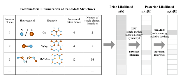
The workflow of our analysis is shown in Fig. 3.
We first generate candidate structures systematically by enumerating all defects that occupy no more than two adjacent atomic sites.
A prior likelihood is then assigned to each candidate structure as an initial guess of how likely the defect structure can appear in the hBN crystal without considering whether it could account for the properties of the SPEs. The prior likelihood can be tailored to describe various experimental scenarios. For example, if carbon impurities are added in the experiment, as shown in recent work 41, one could include the presence of a carbon impurity in the prior likelihood, therefore favoring the posterior likelihood of carbon-containing emitters.
Here, without referring to specific experimental conditions, we choose the prior likelihood on the basis of the structural complexity of the defect, using the single exponential form ,
where measures the complexity of the structure, defined as the number of vacancies and antisite defects plus twice the number of impurities,
is a constant, and is a degeneracy factor due to symmetry-related configurations.
We subsequently combine our computational results with experimental evidence to obtain a posterior likelihood for each structure 40:
| (2) |
where the likelihood function is the probability that the structure is compatible with a specific piece of experimental evidence on the basis of our calculations. The resulting posterior likelihood, which is updated in multiple steps using several computed properties, quantifies which structures among those considered are more likely to be defect emitters in hBN and deserve further consideration.
The properties of the candidate SPE defects and the results of our Bayesian inference analysis are summarized in Table 1.
Moving in the table from left to right, the prior probability is updated to posterior probabilities using calculations presented in subsequent columns.
The first computed posterior probability, , uses the DFT results to infer whether the defect symmetry is compatible with linearly polarized emission
and whether the DFT transition energy, within a standard deviation of 0.5 eV, falls in the 1.62.2 eV emission range found in experiments 10, 34, 11.
The final posterior likelihood in the rightmost column of Table 1 gives the likelihood of the most likely defect structures when all factors have been taken into account,
including comparison between the lowest bright exciton energy and the experimental emission energy and comparison with experiment of the radiative lifetime from our GW-BSE calculations.
The detailed rationale of our Bayesian analysis is described in the Supplementary information.
The main finding from the data in Table 1 is that the defect, which was originally proposed as a SPE in hBN on the basis of DFT calculations 3, 13, 18,
possesses optical and radiative properties that most accurately match the experimental results, even after taking into account excitonic effects and radiative lifetimes.
The next most likely structure is the oxygen impurity defect, , with an emission energy of 1.52 eV just below the experimental range.
On the other hand, we find that the defect, which is also considered a likely candidate in the literature based on DFT calculations 13, 18,
has an emission energy of 2.6 eV that lies too far above the experimental energy range when excitonic effects are included, making it a less likely candidate.
We note that although our analysis excludes the defect and other defects with higher emission energies as candidates for the 1.62.2 eV SPEs, they could still be good candidates for SPEs in the ultraviolet range42, 43, which is not the focus of our discussion.
As the most likely defect emitter in hBN is the structure according to our analysis,
we investigate it in more detail to provide a microscopic understanding of its radiative properties.
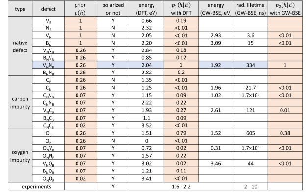
Figure 4(a) shows that the relaxed atomic structure of the defect in monolayer hBN exhibits an out-of-plane displacement of the central nitrogen (N) atom by Å.
If the structure is made planar by constraining the N atom to the hBN plane, the total energy of the system is only moderately higher (by 0.125 eV) than the equilibrium structure.
Therefore the total energy forms a shallow double-well potential as a function of the out-of-plane N atom displacement.
Consistent with recent findings 44, this small energy difference suggests that the structure is soft in the out-of-plane direction and could fluctuate due to external perturbations.
To take this result into account, we compute the optical absorption spectrum of the defect for out-of-plane displacements of the N atom in the 00.83 Å range,
interpolating between the in-plane and out-of-plane equilibrium structures to obtain the intermediate metastable structures.
We find that the absorption spectrum changes drastically for even small changes of , as shown in Fig. 4(c). The spectrum is dominated by two exciton absorption peaks at low energy.
At the equilibrium position ( Å), the first peak at 1.92 eV is associated with a transition from the top valence to the bottom conduction spin-majority electronic states, whose wave functions are shown in Fig. 4(b).
As the displacement of the N atom is decreased from the equilibrium value to zero, which corresponds to a planar structure, the energy of the first exciton peak decreases at first
but then increases again at small values while gaining oscillator strength monotonically.
The second peak at 2.7 eV is also due to a transition from the top valence to the bottom conduction spin-minority bands with relatively large oscillator strength at the out-of-plane equilibrium N atom position.
Both the energy and the oscillator strength of this peak decrease monotonically as decreases [see Fig. 4(c)].
For the planar structure (=0), the second peak becomes the lowest-energy transition but completely loses its oscillator strength and becomes a dark state.
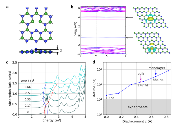
These noteworthy changes in the two lowest-energy exciton peaks are accompanied by substantial changes in the exciton radiative lifetimes. Although the lifetime of the lowest exciton is 334 ns for the DFT equilibrium out-of-plane distortion, it becomes only 19 ns if the structure is kept planar ( case), as shown in Fig. 4(d). This value of the radiative lifetime for the planar structure is within a factor of 23 of experimental results 11. Because many experiments are carried out on thicker hBN samples, we also calculated the radiative lifetime of the defect embedded in bulk hBN (instead of monolayer), a setting resembling more closely SPE experimental measurements in thicker hBN layer stacks (see the Methods section). Due to interlayer interactions, the out-of-plane displacement of the N atom is reduced to Å in bulk hBN. Going from monolayer to bulk reduces the radiative lifetime of the defect to 147 ns due to changes in the dielectric environment and transition dipole, both of which affect the radiative emission rate in Eq. (1). Therefore we conclude that the radiative lifetime of the defect is highly sensitive to both out-of-plane structural distortions and the dielectric environment.
Discussion
While our computed lifetimes are in the 20350 ns range for different structures, these values pertain to an ideal defect with 100% quantum yield,
whereas defect emission measured so far in hBN is likely associated with a lower quantum yield. To explain the discrepancy between the experimental and calculated lifetimes, note that nonradiative processes,
which are not included in our calculation of intrinsic radiative lifetimes, could significantly reduce the apparent lifetime measured in experiments.
For example, a defect with a measured 10 ns lifetime but only a 10% quantum yield would correspond to a 100 ns intrinsic radiative lifetime in very good agreement with our calculations.
Future SPE measurements in hBN taking into account the quantum yield may provide a better estimate of the intrinsic SPE radiative lifetime and enable a more accurate comparison with our calculations.
In summary, we have investigated the excited state and radiative properties of many candidate defect SPEs in hBN.
Our calculations address the photophysics of these defect structures, including their optical transitions and radiative lifetimes,
using calculations that accurately account for excitonic effects and anisotropic dielectric screening.
Our Bayesian statistical analysis allows us to identify the native defect as the most likely candidate within a wide pool of over 20 charge-neutral native defects and carbon or oxygen impurities.
This work explores the fertile ground at the intersection of excited-state first-principles calculations and Bayesian learning methods, and the application of this framework to quantum technologies.
The search for novel single emitters will greatly benefit from such precise first-principles calculations of excited states in materials.
Methods
We carry out DFT calculations in the generalized gradient approximation using the Perdew-Burke-Ernzerhof (PBE) exchange-correlation functional 45. Our spin-polarized DFT calculations employ the plane-wave pseudopotential method implemented in Quantum Espresso 46. The defects are placed in a 55 supercell of hBN with the lattice constant kept fixed at 52.504 Å while the atoms are fully relaxed without symmetry constraints. For calculations on monolayer hBN, a vacuum of 15 Å is used to avoid spurious inter-layer interactions with the periodic replicas. We use ONCV pseudopotentials 47, 48 for all atoms along with a plane-wave kinetic energy cutoff of 80 Ry and a 33 -point Brillouin zone grid. The GW-BSE calculations are carried out with the Yambo code 49, 50 using a 2D slab cutoff of the Coulomb interaction. For calculations of defects in monolayer hBN, a 33 -point grid is employed together with an energy cutoff of 10 Ry for the dielectric matrix. The number of empty bands included in the GW calculation (for the polarizability and self-energy summations) is 7 times the number of occupied bands. These parameters converge the exciton energy to within 0.1 eV in our test calculations, which are shown in the Supplementary information. For calculations on defects in bulk hBN, we use a 551 supercell containing two AA’-stacked layers. The bulk case uses a 223 -point grid; all other parameters are the same as in the monolayer case.
Data Availability
All data needed to evaluate the conclusions in the paper are present in the paper and/or the Supplementary information. Additional data related to this paper may be requested from the authors.
References
- 1 X. Liu, M. C. Hersam, 2D materials for quantum information science. Nat. Rev. Mater. 4, 669–684 (2019).
- 2 X. Chen, X. Lu, S. Dubey, Q. Yao, S. Liu, X. Wang, Q. Xiong, L. Zhang, A. Srivastava, Entanglement of single-photons and chiral phonons in atomically thin . Nat. Phys. 15, 221–227 (2019).
- 3 T. T. Tran, K. Bray, M. J. Ford, M. Toth, I. Aharonovich, Quantum emission from hexagonal boron nitride monolayers. Nat. Nanotechnol. 11, 37–41 (2016).
- 4 A. Gottscholl, M. Kianinia, V. Soltamov, S. Orlinskii, G. Mamin, C. Bradac, C. Kasper, K. Krambrock, A. Sperlich, M. Toth, I. Aharonovich, V. Dyakonov, Initialization and read-out of intrinsic spin defects in a van der Waals crystal at room temperature. Nat. Mater. 19, 540–545 (2020).
- 5 L. Childress, M. V. Gurudev Dutt, J. M. Taylor, A. S. Zibrov, F. Jelezko, J. Wrachtrup, P. R. Hemmer, M. D. Lukin, Coherent dynamics of coupled electron and nuclear spin qubits in diamond. Science 314, 281–285 (2006).
- 6 T. D. Ladd, F. Jelezko, R. Laflamme, Y. Nakamura, C. Monroe, J. L. O’Brien, Quantum computers. Nature 464, 45–53 (2010).
- 7 Loophole-free Bell inequality violation using electron spins separated by 1.3 kilometres. Nature 526, 682–686 (2015).
- 8 I. Aharonovich, D. Englund, M. Toth, Solid-state single-photon emitters. Nat. Photonics 10, 631–641 (2016).
- 9 J. D. Caldwell, I. Aharonovich, G. Cassabois, J. H. Edgar, B. Gil, D. N. Basov, Photonics with hexagonal boron nitride. Nat. Rev. Mater. 4, 552–567 (2019).
- 10 N. R. Jungwirth, B. Calderon, Y. Ji, M. G. Spencer, M. E. Flatté, G. D. Fuchs, Temperature dependence of wavelength selectable zero-phonon emission from single defects in hexagonal boron nitride. Nano Lett. 16, 6052–6057 (2016).
- 11 T. T. Tran, C. Elbadawi, D. Totonjian, C. J. Lobo, G. Grosso, H. Moon, D. R. Englund, M. J. Ford, I. Aharonovich, M. Toth, Robust multicolor single photon emission from point defects in hexagonal boron nitride. ACS Nano 10, 7331-7338 (2016).
- 12 A. Dietrich, M. Bürk, E. S. Steiger, L. Antoniuk, T. T. Tran, M. Nguyen, I. Aharonovich, F. Jelezko, A. Kubanek, Observation of fourier transform limited lines in hexagonal boron nitride. Phys. Rev. B 98, 081414 (2018).
- 13 S. A. Tawfik, S. Ali, M. Fronzi, M. Kianinia, T. T. Tran, C. Stampfl, I. Aharonovich, M. Toth, M. J. Ford, First-principles investigation of quantum emission from hBN defects. Nanoscale 9, 13575–13582 (2017).
- 14 L. Weston, D. Wickramaratne, M. Mackoit, A. Alkauskas, C. G. Van de Walle, Native point defects and impurities in hexagonal boron nitride. Phys. Rev. B 97, 214104 (2018).
- 15 A. Sajid, J. R. Reimers, M. J. Ford, Defect states in hexagonal boron nitride: Assignments of observed properties and prediction of properties relevant to quantum computation. Phys. Rev. B 97, 064101 (2018).
- 16 G. I. López-Morales, N. V. Proscia, G. E. López, C. A. Meriles, V. M. Menon, Toward the identification of atomic defects in hexagonal boron nitride: X-ray photoelectron spectroscopy and first-principles calculations. Preprint at arXiv:1811.05924 .
- 17 G. Noh, D. Choi, J. H. Kim, D. G. Im, Y. H. Kim, H. Seo, J. Lee, Stark tuning of single-photon emitters in hexagonal boron nitride. Nano Lett. 18, 4710–4715 (2018).
- 18 M. Abdi, J. P. Chou, A. Gali, M. B. Plenio, Color centers in hexagonal boron nitride monolayers: A group theory and ab initio analysis. ACS Photonics 5, 1967–1976 (2018).
- 19 M. E. Turiansky, A. Alkauskas, L. C. Bassett, C. G. Van De Walle, Dangling bonds in hexagonal boron nitride as single-photon emitters. Phys. Rev. Lett. 123, 127401 (2019).
- 20 M. Bernardi, M. Palummo, J. C. Grossman, Extraordinary sunlight absorption and one nanometer thick photovoltaics using two-dimensional monolayer materials. Nano Lett. 13, 3664 (2013).
- 21 D. Y. Qiu, F. H. Da Jornada, S. G. Louie, Optical spectrum of MoS2: Many-body effects and diversity of exciton states. Phys. Rev. Lett. 111, 216085 (2013).
- 22 S. Refaely-Abramson, D. Y. Qiu, S. G. Louie, J. B. Neaton, Defect-induced modification of low-lying excitons and valley selectivity in monolayer transition metal dichalcogenides. Phys. Rev. Lett. 121, 167402 (2018).
- 23 C. Attaccalite, M. Bockstedte, A. Marini, A. Rubio, L. Wirtz, Coupling of excitons and defect states in boron-nitride nanostructures. Phys. Rev. B 83, 144115 (2011).
- 24 J. R. Reimers, A. Sajid, R. Kobayashi, M. J. Ford, Understanding and calibrating density-functional-theory calculations describing the energy and spectroscopy of defect sites in hexagonal boron nitride. J. Chem. Theory Comput. 14, 1602–1613 (2018).
- 25 V. Ivády, G. Barcza, G. Thiering, S. Li, H. Hamdi, J.-P. Chou, Ö. Legeza, A. Gali, Ab initio theory of the negatively charged boron vacancy qubit in hexagonal boron nitride. npj Computational Materials 6 (2020).
- 26 M. Rohlfing, S. G. Louie, Electron-hole excitations and optical spectra from first principles. Phys. Rev. B 62, 4927 (2000).
- 27 M. Palummo, M. Bernardi, J. C. Grossman, Exciton radiative lifetimes in two-dimensional transition metal dichalcogenides. Nano Lett. 15, 2794 (2015).
- 28 H.-Y. Chen, M. Palummo, D. Sangalli, M. Bernardi, Theory and ab initio computation of the anisotropic light emission in monolayer transition metal dichalcogenides. Nano Lett. 18, 3839 (2018).
- 29 H.-Y. Chen, V. A. Jhalani, M. Palummo, M. Bernardi, Ab initio calculations of exciton radiative lifetimes in bulk crystals, nanostructures, and molecules. Phys. Rev. B 100, 075135 (2019).
- 30 V. A. Jhalani, H.-Y. Chen, M. Palummo, M. Bernardi, Precise radiative lifetimes in bulk crystals from first principles: the case of wurtzite gallium nitride. J. Phys.: Condens. Matter 32, 084001 (2019).
- 31 R. Loudon, The Quantum Theory of Light (OUP Oxford, 2000).
- 32 H. J. Kimble, M. Dagenais, L. Mandel, Photon antibunching in resonance fluorescence. Phys. Rev. Lett. 39, 691 (1977).
- 33 M. S. Hybertsen, S. G. Louie, Electron correlation in semiconductors and insulators: Band gaps and quasiparticle energies. Phys. Rev. B 34, 5390 (1986).
- 34 A. L. Exarhos, D. A. Hopper, R. R. Grote, A. Alkauskas, L. C. Bassett, Optical signatures of quantum emitters in suspended hexagonal boron nitride. ACS Nano 11, 3328–3336 (2017).
- 35 F. Hayee, L. Yu, J. L. Zhang, C. J. Ciccarino, M. Nguyen, A. F. Marshall, I. Aharonovich, J. Vučković, P. Narang, T. F. Heinz, J. A. Dionne, Revealing multiple classes of stable quantum emitters in hexagonal boron nitride with correlated optical and electron microscopy. Nat. Mater. 19, 534–539 (2020).
- 36 N. Chejanovsky, M. Rezai, F. Paolucci, Y. Kim, T. Rendler, W. Rouabeh, F. Fávaro De Oliveira, P. Herlinger, A. Denisenko, S. Yang, I. Gerhardt, A. Finkler, J. H. Smet, J. Wrachtrup, Structural attributes and photodynamics of visible spectrum quantum emitters in hexagonal boron nitride. Nano Lett. 16, 7037–7045 (2016).
- 37 S. Choi, T. T. Tran, C. Elbadawi, C. Lobo, X. Wang, S. Juodkazis, G. Seniutinas, M. Toth, I. Aharonovich, Engineering and localization of quantum emitters in large hexagonal boron nitride layers. ACS Appl. Mater. Interfaces 8, 29642–29648 (2016).
- 38 P. Cudazzo, I. V. Tokatly, A. Rubio, Dielectric screening in two-dimensional insulators: Implications for excitonic and impurity states in graphane. Phys. Rev. B 84, 085406 (2011).
- 39 K. Andersen, S. Latini, K. S. Thygesen, Dielectric genome of van der Waals heterostructures. Nano Lett. 15, 4616–4621 (2015).
- 40 U. Von Toussaint, Bayesian inference in physics. Rev. Mod. Phys. 83, 943–999 (2011).
- 41 N. Mendelson, D. Chugh, J. R. Reimers, T. S. Cheng, A. Gottscholl, H. Long, C. J. Mellor, A. Zettl, V. Dyakonov, P. H. Beton, S. V. Novikov, C. Jagadish, H. H. Tan, M. J. Ford, M. Toth, C. Bradac, I. Aharonovich, Identifying carbon as the source of visible single-photon emission from hexagonal boron nitride. Nat. Mater. (2020).
- 42 R. Bourrellier, S. Meuret, A. Tararan, O. Stéphan, M. Kociak, L. H. Tizei, A. Zobelli, Bright UV single photon emission at point defects in h-BN. Nano Lett. 16, 4317–4321 (2016).
- 43 Q.-H. Tan, K.-X. Xu, X.-L. Liu, D. Guo, Y.-Z. Xue, S.-L. Ren, Y.-F. Gao, X.-M. Dou, B.-Q. Sun, H.-X. Deng, et al., Ultraviolet to near-infrared single photon emitters in hBN. Preprint at arXiv:1908.06578 .
- 44 S. Li, J.-P. Chou, A. Hu, M. B. Plenio, P. Udvarhelyi, G. Thiering, M. Abdi, A. Gali, Giant shift upon strain on the fluorescence spectrum of color centers in h-BN. Preprint at arXiv:2001.02749 .
- 45 J. P. Perdew, K. Burke, M. Ernzerhof, Generalized gradient approximation made simple. Phys. Rev. Lett. 77, 3865 (1996).
- 46 P. Giannozzi, S. Baroni, N. Bonini, M. Calandra, R. Car, C. Cavazzoni, D. Ceresoli, G. L. Chiarotti, M. Cococcioni, I. Dabo, et al., QUANTUM ESPRESSO: a modular and open-source software project for quantum simulations of materials. J. Phys.: Condens. Matter. 21, 395502 (2009).
- 47 D. R. Hamann, Optimized norm-conserving Vanderbilt pseudopotentials. Phys. Rev. B 88, 085117 (2013).
- 48 M. Schlipf, F. Gygi, Optimization algorithm for the generation of ONCV pseudopotentials. Comput. Phys. Commun. 196, 36–44 (2015).
- 49 A. Marini, C. Hogan, M. Grüning, D. Varsano, Yambo: An ab initio tool for excited state calculations. Comput. Phys. Commun. 180, 1392–1403 (2009).
- 50 D. Sangalli, A. Ferretti, H. Miranda, C. Attaccalite, I. Marri, E. Cannuccia, P. Melo, M. Marsili, F. Paleari, A. Marrazzo, G. Prandini, P. Bonfà, M. O. Atambo, F. Affinito, M. Palummo, A. Molina-Sánchez, C. Hogan, M. Grüning, D. Varsano, A. Marini, Many-body perturbation theory calculations using the yambo code. J. Phys.: Condens. Matter 31, 325902 (2019).
Acknowledgements
We acknowledge valuable discussions with Hamidreza Akbari.
This work was supported by the Department of Energy under Grant No. DE-SC0019166. The radiative lifetime code development was partially supported by the National Science Foundation under Grant No. ACI-1642443.
H.-Y.C. was partially supported by the J. Yang Fellowship. This research used resources of the National Energy Research Scientific Computing Center,
a DOE Office of Science User Facility supported by the Office of Science of the US Department of Energy under Contract No. DE-AC02-05CH11231.
Author contributions
S.G. and M.B. conceived and designed the research. S.G. performed calculation and analysis. H.-Y.C. provided theoretical support. M.B. supervised the entire research project. All authors discussed the results and contributed to the manuscript.
Competing interests
The authors declare that they have no competing financial interests.
Additional information
Supplementary information is available for this paper (at URL to be added).