Substrate screening approach for quasiparticle energies of two-dimensional interfaces with lattice mismatch
Abstract
Two-dimensional (2D) materials are outstanding platforms for exotic physics and emerging applications by forming interfaces. In order to efficiently take into account the substrate screening in the quasiparticle energies of 2D materials, several theoretical methods have been proposed previously; but only applicable to interfaces of two systems’ lattice constants with certain integer proportion, which often requires a few percent of strain. In this work, we analytically showed the equivalence and distinction among different approximate methods for substrate dielectric matrices. We evaluated the accuracy of these methods, by applying them to calculate quasi-particle energies of hexagonal boron nitride interface systems (heterojunctions and bilayers), and compared with explicit interface calculations. Most importantly, we developed an efficient and accurate interpolation technique for dielectric matrices that made quasiparticle energy calculations possible for arbitrarily mismatched interfaces free of strain, which is extremely important for practical applications.
I Introduction
Two-dimensional (2D) materials and their interfaces have shown unprecedented rich physics and promising applications in many areas, such as opto-spintronics Wolf et al. (2001); Žutić et al. (2004), quantum information He et al. (2015); Tran et al. (2016), and biomedical research Wang et al. (2015); Sun et al. (2015). New emerging phenomena such as non-conventional superconductivity Cao et al. (2018a, b) or topologically protected states Song et al. (2019); Ahn et al. (2019); Qin and Zhang (2014); Qin et al. (2019) may be created by stacking 2D layers. Experimentally, growth of 2D materials, achieved through physical epitaxy or chemical vapor deposition (CVD), is typically supported on a substrate Novoselov et al. (2016). In general, the electrical and optical properties of 2D materials could be strongly modified by substrate screening. For example, the 2D materials’ fundamental electronic gap can be significantly reduced due to the dielectric screening from surrounding layers (substrates) when forming heterointerfaces Winther and Thygesen (2017); Ugeda et al. (2014). Reliable prediction of substrate screening effects from first-principles calculations is critical for accurate interpretation of experimental results and guidance of new materials’ design.
Currently, widely-used electronic structure methods such as the HSE06 hybrid functional Krukau et al. (2006) may accurately describe a large number of three-dimensional bulk systems, but are inadequate for low dimensional systems such as ultrathin 2D materials because of their highly inhomogeneous dielectric screening. The Koopman’s compliant hybrid functional Stein et al. (2010); Nguyen et al. (2018); Weng et al. (2018) or dielectric dependent hybrid functional Zheng et al. (2019) are necessary for the electronic structure of ultrathin 2D materials, where the fraction of Fock exchange varies with the number of layers Smart et al. (2018) and needs to be determined for each individual material and thickness.
On the other hand, many-body perturbation theory (MBPT) Ping et al. (2013a); Hybertsen and Louie (1987); Sangalli et al. (2019) can successfully describe the quasiparticle properties of 2D materials such as fundamental electronic gaps, regardless of their thickness and dielectric properties. Generally, one and two-particle excitations, experimentally corresponding to charged excitations (e.g. photoemission) and neutral excitation (e.g. optical absorption), can be accurately obtained by the GW approximation Hedin (1999); Ping et al. (2013a); Wu et al. (2017); Govoni and Galli (2015); Pham et al. (2013) and the Bethe–Salpeter equation Rohlfing and Louie (2000); Wu et al. (2019a); Ping et al. (2012, 2013b); Rocca et al. (2012, 2010) (BSE), respectively. However, explicit interface calculations at this level of theory are extremely computationally demanding and not suitable for the rapid evaluation of the effect of different substrates.
Therefore, several approximate methods have been proposed to compute the quasiparticle properties of interfaces at the cost of primitive cell calculations of the subsystems composing the interface Trolle et al. (2017); Yan et al. (2011); Ugeda et al. (2014). Typically, for weakly-bonded Van de Waals (vdW) interfaces, the hybridization between layers is relatively weak and the dominant effect of the substrate consists in modifying the dielectric screening of the material of interest Yan et al. (2011). Within the GW approximation, this effect can be described by approximating the dielectric matrix of an interface in terms of contributions from individual subsystems (the material and the substrate), as proposed in several previous studies Trolle et al. (2017); Yan et al. (2011); Ugeda et al. (2014). Despite the reasonable level of accuracy achieved through these methods, the underlying approximations and connections between different methods have not been carefully evaluated. For example, partially neglecting local-field effect of substrate dielectric screening (i.e. removing in-plane and/or out-of-plane off-diagonal elements of dielectric matrices Ugeda et al. (2014); Bradley et al. (2015); Qiu et al. (2017)) has been a common approximation previously, which was not carefully examined before. We will test the applicability of such approximation in different systems, for both in-plane and out-of-plane components of dielectric matrices.
Most importantly, previous methods can not be applied to arbitrarily lattice-mismatched 2D interfaces, namely an integer relation between lattice constants is necessary (, where and are the primitive lattice constants of the two systems at interfaces, and is an integer number). Forcing lattice-matching or the fulfillment of the above relation is typically required for interface calculations. These constraints either limit the choice of interfaces that can be studied or require applying artificial strain that may strongly modify the electronic structure. In this work, we develop a reciprocal-space linear-interpolation method in the entire space to approximate interface dielectric matrices of arbitrarily mismatched systems. This approach makes MBPT calculations of general interfaces possible and free of strain.
In order to demonstrate the accuracy and efficiency of this new methodology, we will consider applications to interfaces involving hexagonal boron nitride (hBN). This material has a wide band gap in ultraviolet region, with promising applications in deep ultraviolet light-emitting devices Kubota et al. (2007) and as a host for spin qubits and single photon emitters Wu et al. (2019b) in quantum information technologies Awschalom et al. (2013); Wu et al. (2017). As ultrathin hBN is mostly supported on substrates in experimental measurements, it is critical to accurately predict the effect of substrates on electronic structure of hBN. This is also important for evaluations of defect properties in 2D materials supported by substrates Abidi et al. (2019); Wang and Sundararaman (2019). We will use hBN with SnS2 substrates and bilayer hBN in two conformations as prototypical examples for our methodology validation in this study.
For the rest of the paper, we first analytically derived the connection among different approximations of dielectric matrices with substrate screening Yan et al. (2011); Ugeda et al. (2014); Qiu et al. (2017); Xuan et al. (2019); Liu et al. (2019). We then performed the separate GW calculations for subsystems from interfaces with several approximate approaches to construct the interface polarizability, and compared results with explicit interfaces in order to evaluate the accuracy of these methods. Next we examine the importance of off-diagonal elements of polarizability in substrate screenings in various 2D interface systems. Finally, we introduced our linear-interpolation technique, benchmarked it and showed the quasiparticle energies obtained by this technique for arbitrarily lattice-mismatched 2D interfaces.
II Methodology
In this section, we will discuss the different methods and concepts used in this paper, which are summarized in the Table 1.
| Methods | Assumption |
|---|---|
| -sum (Eq. 3) | Coulomb interaction between layers |
| -sum | Uses interface eigenvalue |
| in -sum | |
| -sum | Uses interface eigenvalue |
| and wavefunctions in GW with -sum | |
| -sum (Eq. 4) | Coulomb interaction between layers, |
| equiv. to -sum at RPA | |
| -sum (Eq. 6) | No interaction between layers |
| Approximations | Definition |
| -diag | Neglects off-diagonal elements |
| -diag | Neglects off-diagonal elements |
| Interface structure | Solution |
| Lattice match | Direct summation |
| Special match | mapping |
| Arbitrary mismatch | bilinear interpolation |
II.1 Methods for interface polarizability
The interactions among quasi-particles within the GW approximation is described by the screened Coulomb potential , where is the bare Coulomb interaction and is the dielectric matrix. The inverse dielectric matrix is defined by within the random phase approximation (RPA) Hybertsen and Louie (1987). The reducible polarizability can be obtained from the irreducible polarizability (also known as independent-particle polarizability) through the equation .
For the purpose of our discussion we first partition the total (“tot”) vdW interface systems into material (“m”) and substrate (“s”) subsystems Yan et al. (2011). Considering density response of external field, we obtain:
| (1) |
where is the density response, and the reducible polarizability is defined as the density-density response function to an applied potential. If we consider the material subsystem (“m”) as the probe, the total external potential includes the external applied potential () and the Coulomb potential from the charge response in the substrate (). (We assume the material and substrate are connected only through interlayer Coulomb interactions, with minimum wavefunction overlap between material and substrates, i.e. interlayer hybridization.) Then we define an effective polarizability as a density response function of one subsystem to only the external applied potential (), i.e. . More precisely, can be given in terms of through Eq. 1:
| (2) |
When subsystems have negligible interlayer wavefunction overlap (i.e. hybridization), the total density response () can be written as and then the total polarizability of entire interface systems is
| (3) |
In summary, this approach uses the reducible polarizabilty of each subsystem () where the Coulomb potential from the other subsystem is considered part of external potential in Eq. 1, to construct the effective reducible polarizability of each subsystem where such potential is excluded from external potential in Eq. 2. Then we sum up and to obtain total reducible polarizability of interface systems in Eq. 3, which will be denoted as “-sum”.
As we noted above, interlayer wavefunction overlap or hybridization effect is not taken into account in the method described above. The hybridization effect can change the eigenvalues and eigenfunctions at the DFT level which then change the Green’s function (G) and dielectric matrix (in W) in the GW calculations. Therefore, for systems with strong interlayer hybridization, we can add the hybridization effect step-by-step. We can add corrections from ground state eigenvalues of interfaces to the -sum methods, namely “-sum” method, which partially take into account the effect of interlayer hybridization on eigenvalues at the DFT level. Furthermore, we can also include interface ground state wavefunction (“FWF”) and eigenvalues as inputs for Green’s function (G), denoted as “-sum” method. This method is close to GW calculations of an explicit interface except with approximate dielectric matrix by Eq. 3.
From another perspective, if the interlayer hybridization or wavefunction overlap is negligible (similar to the condition required above for ) Liu et al. (2019); Xuan et al. (2019), the total irreducible polarizability of the interfaces can be expressed approximately as the sum of each subsystem contribution Bradley et al. (2015); Ugeda et al. (2014); Qiu et al. (2017); Naik and Jain (2018); Xuan et al. (2019); Liu et al. (2019)
| (4) |
which we denote as “-sum” method. To further understand the theoretical connection between different methods, we rewrite Eq. 1 with through relation as:
| (5) |
Here as the irreducible polarizability is the density response function to total field , which includes the applied field and bare Coulomb potential of the total interface system, namely . Using the above condition for the interface, summation of the two equations of subsystems in Eq. 5 results in , which gives Eq. 4. This indicate that the -sum method and -sum method are equivalent under RPA. However, -sum method and -sum method are not equivalent when the diagonal approximation is applied, i.e. neglecting off-diagonal elements of in the former or in the latter, as we will discuss in the Sec. II.B. Therefore we primarily used -sum method in this paper.
If we further neglect the interlayer Coulomb interaction, this will set to zero in Eq. 1 and lead . This is at the non-interacting limit between two layers, where
| (6) |
and we name it as “-sum” method. In Sec. IV.1, we will compare the quasiparticle energies of interfaces with the above approximated dielectric matrices with explicit interface GW calculations.
II.2 Diagonal approximation of dielectric screening
For simple metals which may be treated as “jellium”, the nearly translational invariance justifies the dielectric matrix may be diagonal in reciprocal space Hybertsen and Louie (1987). However, semiconductors and insulators have strong in-homogeneity at interaction length scale requires non-zero off-diagonal elements of Resta and Baldereschi (1981); Hybertsen and Louie (1987). The effect from off-diagonal elements of dielectric matrix is often referred to the “local field effect” Ceperley and Alder (1980); Resta and Baldereschi (1981); Hybertsen and Louie (1987).
While the effect of off-diagonal terms in intrinsic dielectric screening has been systematically studied Ceperley and Alder (1980); Resta and Baldereschi (1981); Hybertsen and Louie (1987), the off-diagonal terms’ effect from environmental dielectric screening has not been studied in detail. Here we will investigate the off-diagonal effect of environmental dielectric screening through two different approaches, i.e. by applying the diagonal approximation of dielectric matrix (“-diag”, which directly relates to diagonal approximation of ) or inverse dielectric matrix (“-diag”, which directly relates to diagonal approximation of and ).
The -diag approximation has been used for substrate dielectric screening in the past work Bradley et al. (2015); Ugeda et al. (2014); Qiu et al. (2017); Naik and Jain (2018) when applying the -sum method, specifically, by removing the in-plane off-diagonal components of substrate dielectric matrices. The -diag approximation has not been employed before, but is more convenient in the -sum approach. Since the off-diagonal elements of will contribute to the diagonal elements of and through the matrix inverse operation, this is a weaker approaximation than -diag. We will compare these two approximations considering specific numerical examples in Sec. IV.2.
II.3 Reciprocal-space linear-interpolation approach
The construction of interface structure models is often complicated by the problem of lattice matching between two subsystems. One of the main objectives of this work is to propose a general approach that can be applied to subsystems with rather different periodicity and crystal symmetry, and does not require the application of strain to force the lattice matching at the interface.
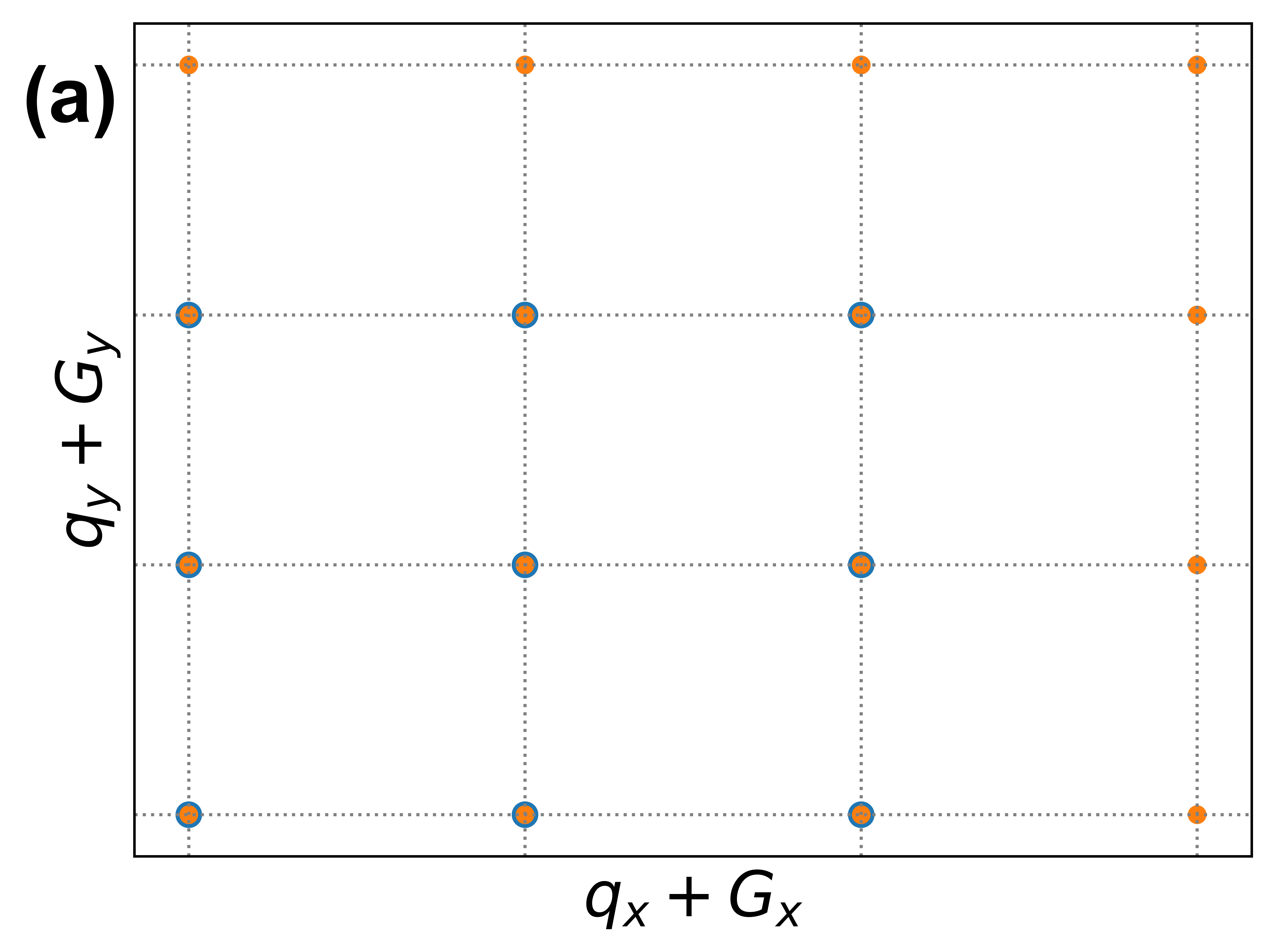
In general, in order to directly sum the subsystem contributions to obtain the polarizability (and dielectric matrix) of the full interface, one needs an exact correspondence of the vectors between the material and the substrate. This requires finding two integer numbers and such that the lattice constants (substrate) and (material) satisfy the relation . If and can be chosen to be reasonably small, calculations can be directly performed for supercells containing and repetitions, although this approach often requires the application of a small percentage of strain. However, if the required or are large, several methods have been proposed to make this type of calculations practical Bradley et al. (2015); Ugeda et al. (2014); Qiu et al. (2017); Naik and Jain (2018); Xuan et al. (2019); Liu et al. (2019). The central idea is to consider unit cells only and to perform a one to one mapping between the reciprocal space vectors of the material and substrate Liu et al. (2019) (see Figure 2(a)). This approach still requires the relation to be satisfied (possibly by applying a small strain to modify or ) but avoids supercell calculations. We note that even if one applies the diagonal approximation for or , the diagonal elements still contain both and vectors, which requires this relation to be satisfied. While this is a clear numerical improvement, a large number of vectors in the first Brillouin zone might still be required. Indeed, one needs to sample and/or point meshes fine enough to ensure that the number of points () satisfy the relation or equivalently . Accordingly, this approach becomes computationally demanding for large and/or . A more serious issue is that this mapping scheme is not possible for interfaces with two systems with very different crystal symmetry, e.g. a hexagonal and a lattice.
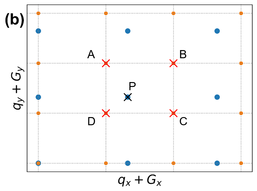
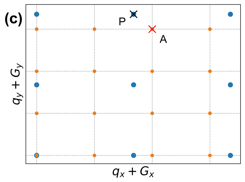
In this work we propose a general method for arbitrarily lattice-mismatched interfaces where it is not possible to map the vectors between the two subsystems. This approach applies a linear interpolation of the matrix elements on the substrate grid (, ) to obtain their representation on the material grid (, ), as shown in Figure 2(b) and (c). We note that we need to interpolate together between materials and substrates, which can completely remove the symmetry constrain. Interpolation of only as done in the past work Felipe et al. (2017); Kammerlander et al. (2012) will improve -sampling convergence speed but does not solve the periodicity or symmetry mismatch problem at interfaces. As this procedure requires a sampling of the vectors over the full first Brillouin zone (FBZ), whenever necessary, the symmetry operators are used to reconstruct the grid in the FBZ from the grid in the irreducible Brillouin zone (IBZ). Without loss of generality we choose the same size for vacuum in the -direction for both subsystems; in this way the same out-of-plane reciprocal lattice components are obtained. In order to simplify the implementation, we neglect the in-plane off-diagonal elements of the substrate, i.e. we consider . As shown later for specific numerical examples (see Sec. IV.3), this approximation works well in practice for mismatched 2D interfaces. For each set of matrix elements at fixed , the standard bilinear interpolation technique Press et al. (2007) is used to obtain the corresponding in-plane matrix elements in the material subspace, interpolated from in the substrate subspace. As shown in Figure 2(b), the value of the response function at each point (denoted by the black cross overlaying the blue dots) is obtained by interpolating the values at the four nearest points (denoted by the red cross overlaying the orange dots). We note that the bilinear interpolation method can be applied only if all four nearest neighbours exist within the boundaries of space; otherwise the standard proximal interpolation method is applied, which considers only the nearest point on the grid (most likely at the boundary), as shown in Figure 2(c). However, the values close to the boundary of space are very close to zero as shown in Figure 3(a).The bilinear interpolation method is fully general regardless of crystal symmetry, which can be applied to arbitrary interfaces.
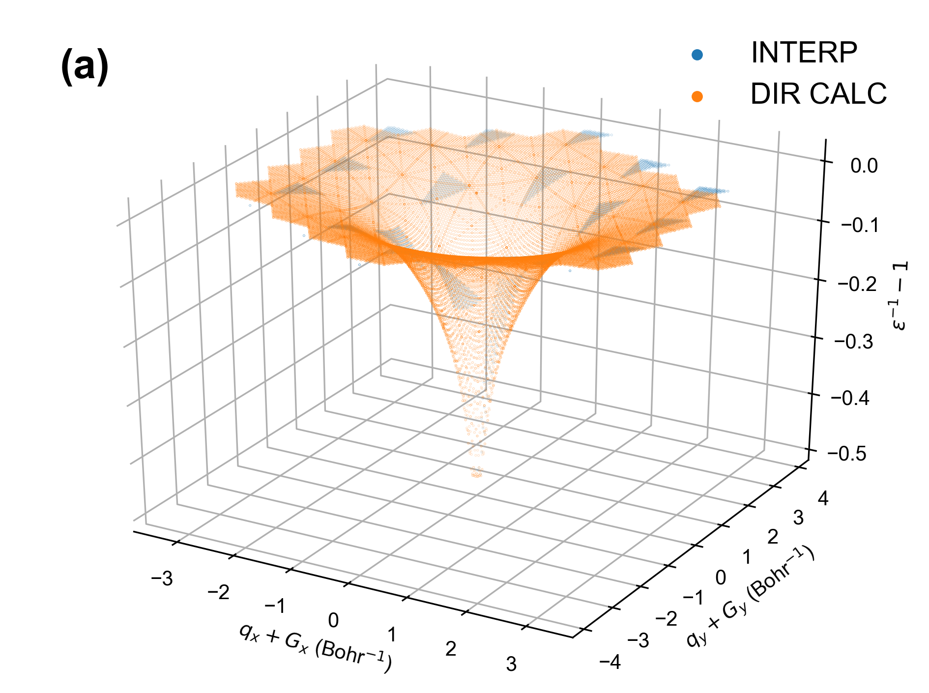
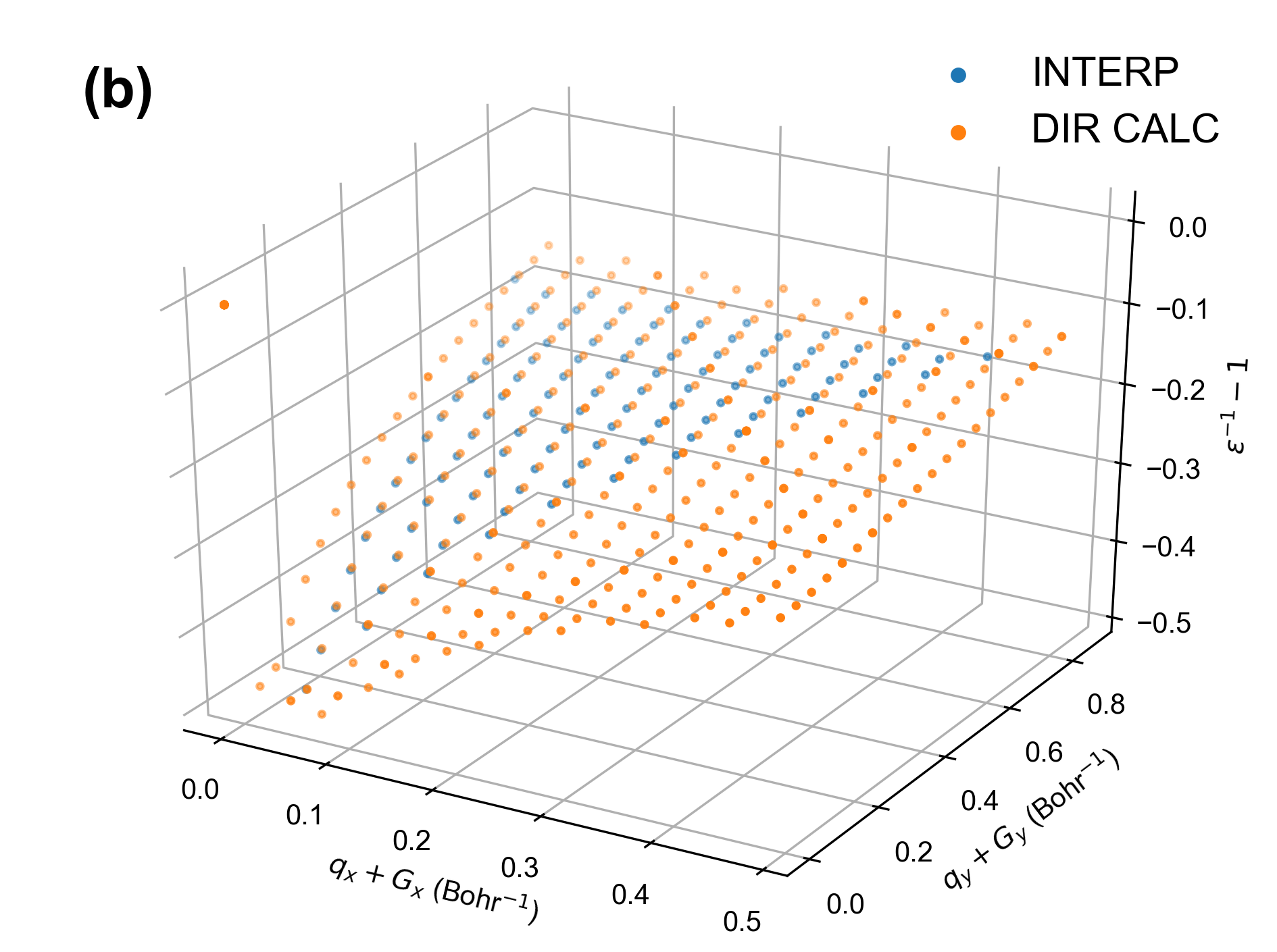
By applying the interpolation method, we can obtain substrate matrix elements at the material’s grids, without any artificial strain Liu et al. (2019); Ugeda et al. (2014); Xuan et al. (2019). As shown in Figure 3(a), the orange points are the values computed at the substrate momentum space with full BZ, then we interpolate them to the blue points on the grids of material momentum space (only elements in IBZ are shown here). The blue points fall smoothly on the surface of orange points which show a good interpolation quality. A zoomed-in picture is also shown in Figure 3(b). To show the generality of our method, we applied this interpolation method for hBN/phosphorene(BP) interface, where BP has a rectangle lattice, sharply different from the hexgonal lattice hBN has (see SI Figure 1). We show again with our interpolation method, one can obtain the matrix elements of substrates at the material grids. Then we can compute the quasiparticle energies of this interface, at two systems’ natural lattice constants, with the -sum method.
III Computational details
III.1 Computational workflow
The workflow of GW calculations for the interface is structured as follows. We first compute the reducible polarizabilities () for each subsystem separately and then we use them to obtain the effective polarizabilities () using Eq. 2. In case of lattice mismatch between the two subsystems, the matrix elements of the polarizability of the substrates are obtained on the same reciprocal space grid of the material (ML hBN in the practical applications of this work) by using the linear interpolation method described above. Next we sum them to obtain (i.e. the -sum method).
Finally, in order to include the screening effect of the substrate on the material, the GW calculations are performed for the standalone hBN ML with the obtained in the previous step. As we will discuss later, one can achieve further improvement for interfaces with strong hybridization by including corrections from ground state eigenvalues and wavefunctions of explicit interfaces.
III.2 Numerical parameters
In this work, we mainly focus on the quasiparticle energies of monolayer hBN/substrate interfaces as prototypical systems (where as substrates we will consider monolayer hBN itself and monolayer SnS2). Density functional theory (DFT) ground state calculations based on the Perdew-Burke-Ernzerhof (PBE) exchange-correlation functional Perdew et al. (1996) have been performed using the open source plane-wave code Quantum ESPRESSO Giannozzi et al. (2017) with Optimized Norm-Conserving Vanderbilt (ONCV) pseudopotentials Hamann (2013) and a 80 Ry wave function cutoff. From structural relaxation we obtained lattice constants of 2.51 (Å) and 3.70 (Å) for the free-standing monolayer (ML) hBN and SnS2, respectively.
GW calculations with the Godby-Needs plasmon-pole approximation Godby and Needs (1989); Oschlies et al. (1995) (PPA) were then performed using the Yambo Marini et al. (2009) code. We chose PPA as a showcase for lower computational cost, but we can apply the same -sum and reciprocal-space interpolation method with full frequency integration as well without technical difficulty, with more computational cost. Importantly, to the best of our knowledge, only PPA models or static COHSEX approximation were used in past calculations for the dielectric screening of substrates Yan et al. (2011); Ugeda et al. (2014); Bradley et al. (2015); Qiu et al. (2017); Xuan et al. (2019); Liu et al. (2019); Naik and Jain (2018) and the obtained results were reasonably accurate. We used the same plasmon frequency for all calculations =27.2 eV and found little variation of the results (i.e. within 20 meV, with from 24.5 to 30 eV).
The distance between the nearest periodic repetitions along the vacuum direction was set to be 20 Å. In order to speed up convergence with respect to vacuum sizes, a 2D Coulomb truncation technique was applied to dielectric matrices and GW self-energies Rozzi et al. (2006). For bilayer hBN systems, we set the interlayer distance to the bulk value of 3.33(Å) for both of the two different stacking configurations considered here ( and ). The hBN/SnS2 interlayer distance was set to 3.31 (Å) as obtained from structural relaxation with vdW-corrected functionals Grimme (2006); Barone et al. (2009).
For each free-standing monolayer (“ML”) unit cell, the GW self-energy cutoff is set to 15 Ry. The number of bands is set to 1000 (1500) for hBN (SnS2) unit cell calculations. The exchange self-energy cutoff is set to 40 Ry. We use a () -points sampling for ML-hBN (ML-SnS2) unit cell calculations, unless specified.
GW calculations for the full explicit heterointerfaces have also been performed to obtain “exact” reference results to benchmark the different methods for the substrate screening effects (see Sec. IV.1). The computational parameters for the full interface are set to keep consistency between supercells and unit cell calculations. Additional computational details and convergence tests can be found in SI 111See Supplemental Material at [URL will be inserted by publisher], for additional details on examples of interpolation method for arbitrarily mismatched interface, numerical parameters and convergence of GW calculations Birowska et al. (2019); Gao et al. (2016); Qiu et al. (2016); Wu et al. (2017); Rozzi et al. (2006)..
IV Results and discussions
IV.1 Numerical comparison of different methods for substrate screening
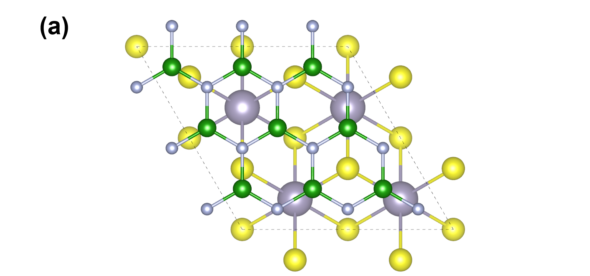
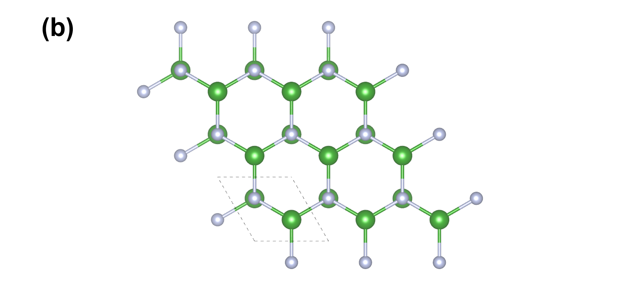
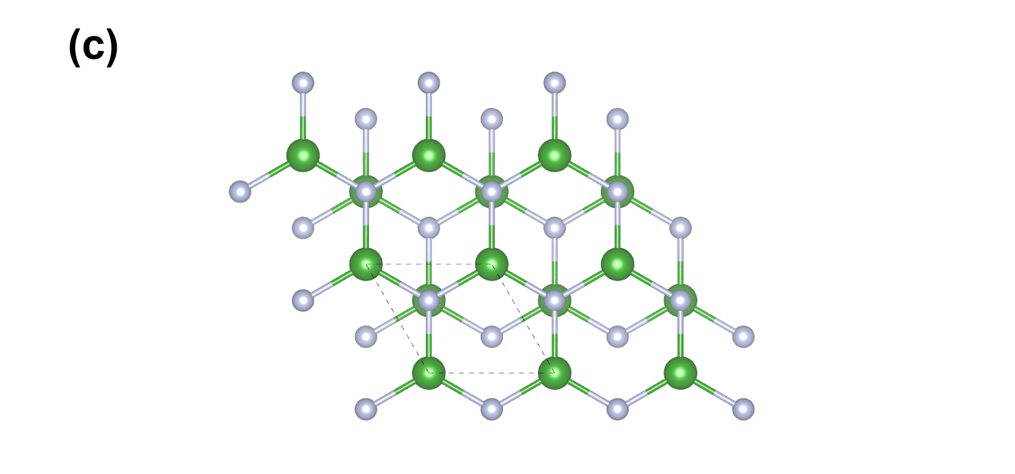
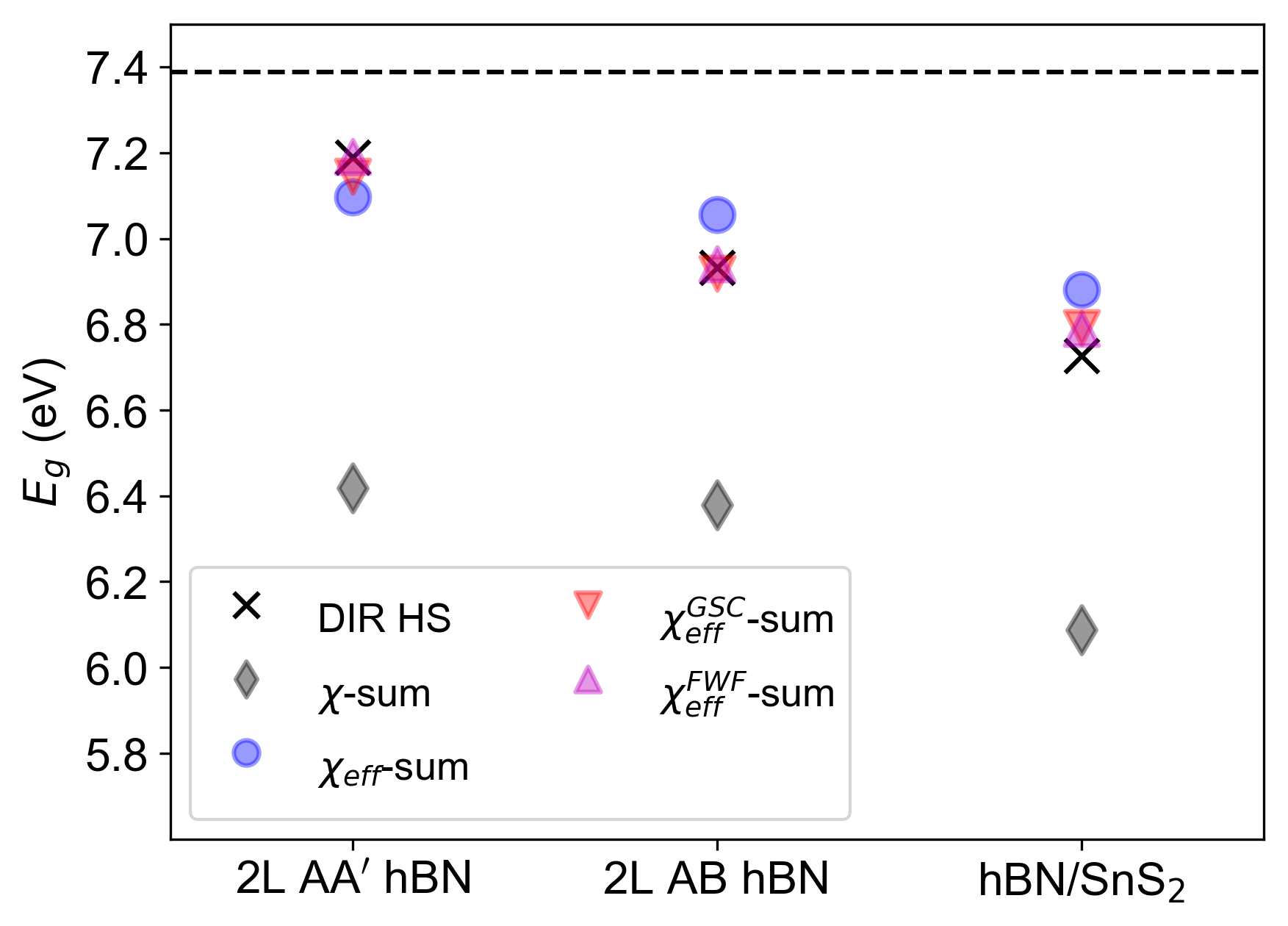
After presenting in Sec. II with different approaches to approximate the total dielectric screening of an interface between two weakly interacting subsystems, in this section we discuss their accuracy in practical GW calculations. Results for explicit interfaces will be used as a reference. Specifically, we computed the GW quasiparticle bandgaps of three interfaces: hBN/SnS2, 2L-AB stacking hBN with two layers’ atoms misaligned, and 2L-AA′ stacking hBN interface with two layers’ atoms aligned (the corresponding atomic structures are shown in Figure 1). In order to keep the comparison of different methodologies as simple as possible, the calculations in this section are performed with fully commensurate interfaces, for both explicit and approximate interface calculations, as the results shown in Figure 4.
From the explicit interface results in Figure 4 we see that the direct band gap of hBN at the hBN/SnS2 interface (black cross in the third column) is reduced by 0.8 eV compared with the isolated ML hBN (dashed line). This value is about four times of the band gap reduction for the bilayer hBN with respect to the isolated ML hBN (black cross in the first and second columns). This is because ML SnS2 has a much stronger dielectric screening ( ) and a smaller electronic band gap ( eV) compared to ML hBN, which has and an electronic band gap of eV. This indicates the positive correlation between electronic band gap reduction and substrate dielectric screening, similar to previous discussions Cho and Berkelbach (2018); Olsen et al. (2016); Jiang et al. (2017).
Secondly, we find that the effective polarizability approach results (“-sum” method, blue circle) are consistently in good agreement with the ones from explicit interface GW calculations (“Direct”, black cross), i.e. within 0.2 eV. We improve the agreement by 50 meV with additional corrections from ground state eigenvalues of interfaces (“-sum” method, red triangle), which partially take into account the effect of interlayer couplings on eigenvalues at the DFT level. Moreover, by using interface ground state wavefunctions and eigenvalues (“FWF”) as inputs for Green’s function calculations, the results of the effective polarizability approximation (“-sum” method, green square) are further improved, i.e. with only 10 meV difference from the explicit interface GW calculations. While a similar approach was used in Ref. 44, the -sum method has a computational cost similar to that of the full interface GW calculation (although the evaluation of the dielectric matrix is more efficient) and is much more demanding than the other methods in Figure 4 and Table 1. Therefore -sum and -sum provide the best compromise between accuracy and computational cost. We note that for explicit hBN/SnS2 interface, we had to apply 1.5% strain to obtain commensurate supercells which may explain why this interface has slightly larger difference between -sum and explicit calculation than bilayer hBN.
In sharp contrast to the methods discussed above, the non-interacting interlayer method based on Eq. 6 (“-sum” method, black diamond) gives results far from the explicit interface reference (e.g. with an error of about 0.6 eV). This indicates that the interlayer Coulomb interaction plays a dominant role in the electronic bandgap reduction by substrate screening.
IV.2 Diagonal approximation of substrate dielectric screening
In this section we will compare different diagonal approximations for the screening considering different numerical examples. With “in-plane -diag” we will denote an approximation that discards the in-plane off-diagonal elements of reducible polarizability in reciprocal space, i.e. . Similarly, “out-of-plane -diag” will denote an approach that does not include the out-of-plane off-diagonal elements of polarizability in reciprocal space, i.e. . Analogous definitions will be used for -diag.
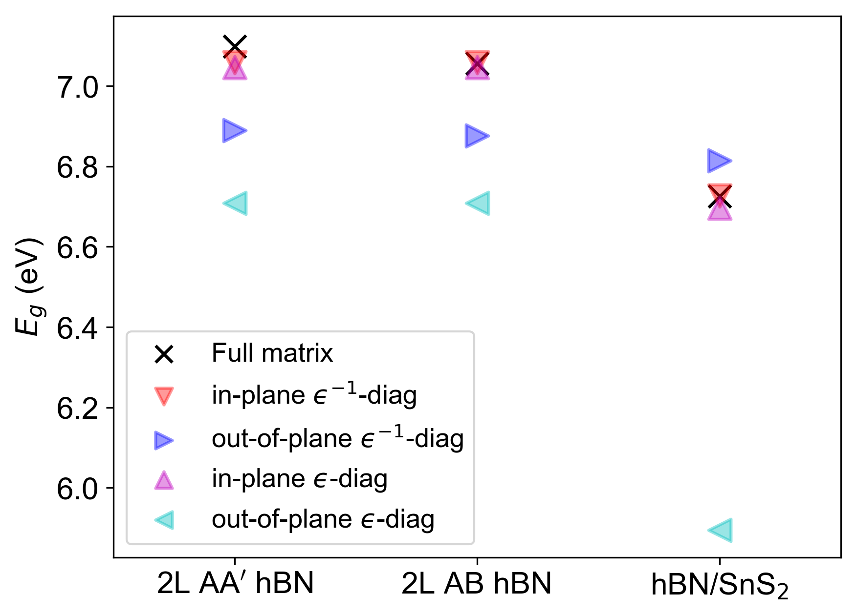
The GW quasiparticle gaps with different diagonal approximations for the hBN bilayer in two different confomations (AA′/ AB) and the hBN/SnS2 interface are shown in Figure 5. We find that for both the and diagonal approximations, neglecting out-of-plane off-diagonal elements of the substrate (“out-of-plane -diag” and “out-of-plane -diag”, dennoted by dark blue right triangle and light blue left triangle, respectively) causes a large discrepancy of the bandgaps (i.e. from 0.2 to 0.8 eV) with respect to the “exact” result obtained from the full screening matrix (“Full matrix”, black cross). In contrast, the results obtained by neglecting in-plane off diagonal elements (in-plane / in-plane -diag, red down triangle/ magenta up triangle) are similar to those with the full screening matrix with deviations within 50 meV. This means the inhomogeneity effect of out-of-plane substrate screening on quasiparticle energies is much stronger than the one of in-plane substrate screening, because the out-of-plane direction is along the non-periodic (vacuum) direction with dramatically inhomogeneous charge distribution, compared to the in-plane periodic direction.
Besides the overall difference of diagonal approximation along different directions, we also distinguish the difference between -diag and -diag approach in each case. 1) Along the in-plane direction, the difference between different approaches is negligible, i.e. less than 10 meV. 2) Along the out-of-plane direction, the out-of-plane -diag results (dark blue right triangle) are much closer to the full dielectric matrix results (black cross) than the out-of-plane -diag results (light blue left triangle) in Figure 5. This is consistent with our earlier speculation that the -diag may be a better (weaker) approximation, because the off-diagonal elements of irreducible polarizability contribute to or during its matrix inversion, which is completely missing in the -diag approximation.
Moreover, the in-plane inhomogeneity is relatively larger when there is stronger interlayer coupling with atoms aligned perfectly for chemical bonding. For example, the in-plane inhomogeneity of bilayer hBN with atoms aligned (e.g. 2L AA′ hBN in Figure 1 (b); both in-plane -diag (red down triangle) and in-plane -diag (magenta up triangle) results have 40 meV difference from the “Full matrix” results in the first column of Figure 5), is larger than the interfaces with atoms misaligned (e.g. 2L AB hBN and hBN/SnS2 hectorstructure in Figure 1 (a) and (c); both in-plane -diag and in-plane -diag results have no difference from “Full matrix” results in the second and third columns of Figure 5).

IV.3 Lattice mismatched hBN/SnS2 interface
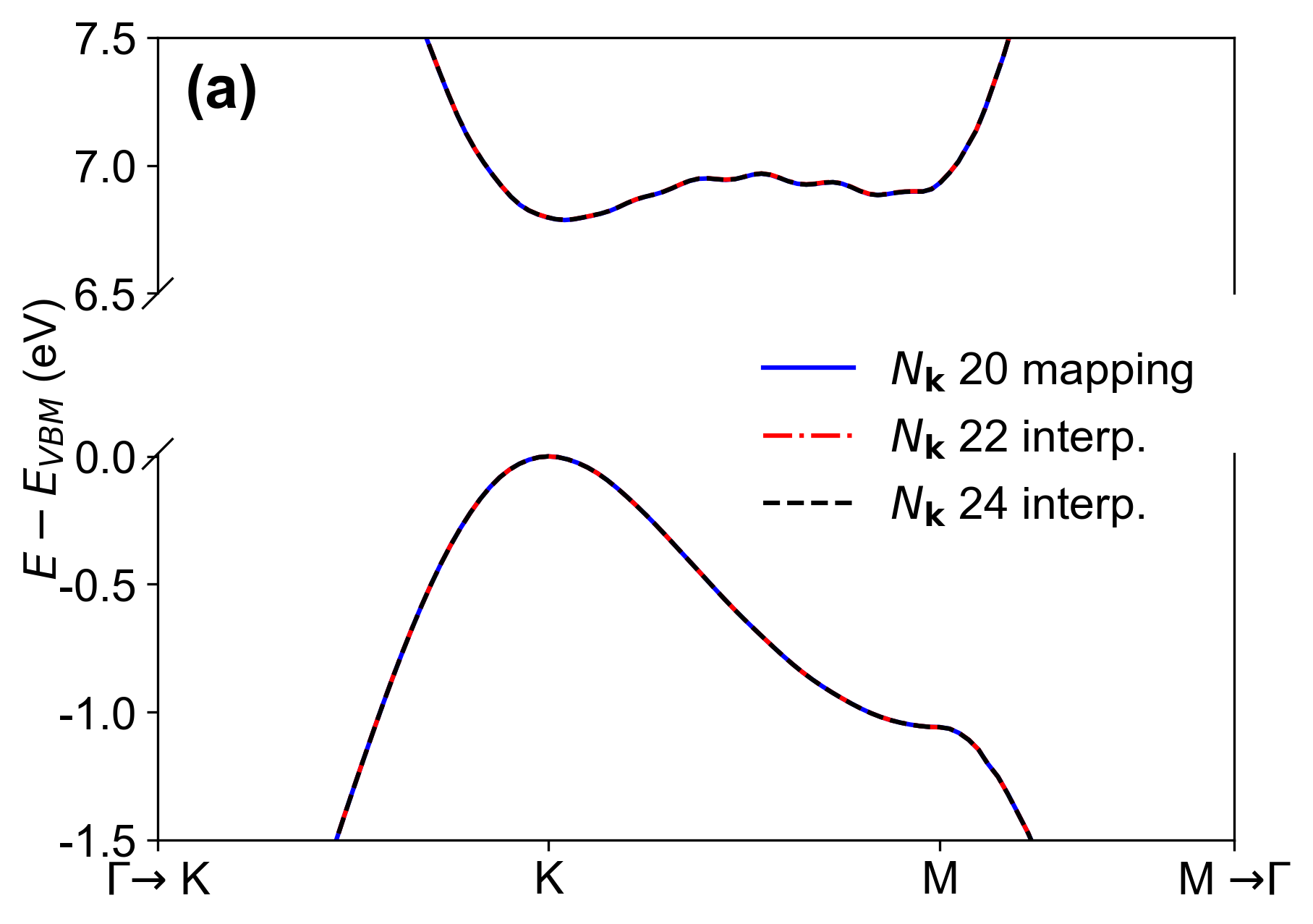
In order to benchmark the reciprocal-space linear-interpolation method introduced in Sec. II.3 and Table 1, we consider the hBN/SnS2 interface. A strain of 1.5% was applied to SnS2 to match the hBN lattice constant with a 2:3 ratio in each direction of the plane (namely ). By using a commensurate -point sampling for the two subsystems with a 2:3 ratio, a mapping of the vectors is possible and traditional methods for the substrate effect can be applied to produce a reference results for our new interpolation method (which, instead, will be used with an incommensurate -point sampling). We computed the GW band edges near the high symmetry point of hBN on the SnS2 substrate with the -sum method at different -point samplings, as shown in Figure 6. The mesh for -point sampling was chosen to be identical to the -point sampling. Specifically, the reference calculations were performed with the hBN unit cell calculation with and -point sampling for the units cells of SnS2 and hBN, respectively (this choice satisfies the 2:3 ratio for each inplane direction). The reference result obtained from the mapping is shown in Figure 6 (blue curve labelled by “ 20 mapping”). To apply our interpolation technique, it is not necessary to use commensurate grids and we compare instead the results for two different choices of the -point sampling for SnS2. Specifically, in Figure 6 we show the results for the (red dashed line, “ 22 interp.”) and (black dashed line, “ 24 interp.”) -point grids, which do not allow for a mapping of the reciprocal space vectors and would be impossible to treat without our interpolation method. The results in Figure 6(a) show that the GW band structure with interpolation (red and black dashed lines) is nearly identical to the one based on the mapping (blue solid line), with differences smaller than 1 meV (as can be seen by zooming-in the conduction band edge in Figure 6(b)). This comparison demonstrates the excellent numerical accuracy of our linear interpolation method, which could have also been expected from the high quality of the interpolation in Figure 3.
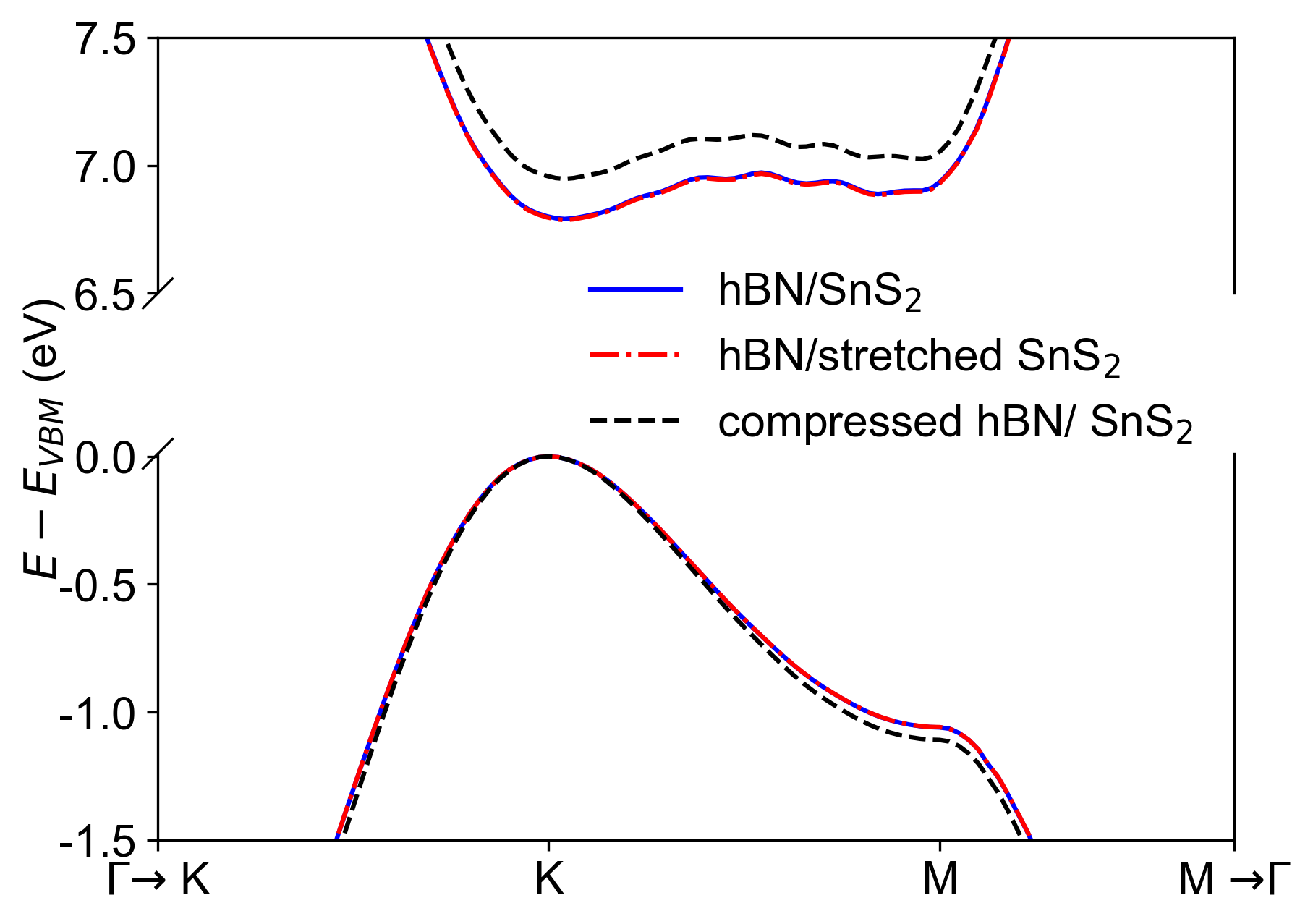
Finally, we use our new interpolation method to better understand the effect of the strain on quasiparticle energies. In Figure 7, the blue curve corresponds to the the hBN bandstructure on the SnS2 substrate without strain for either system as obtained from the interpolation scheme described above. These results are compared with those obtained for the interface by applying strain either to compress the hBN lattice parameter or to stretch SnS2. We found that even a 1.5 compressive strain for hBN (black dashed line), the conduction band edge changes by 0.2 eV. Since we are focusing on the band structure of hBN states, the application of the strain to the SnS2 substrate leads to negligible changes (red dash-dotted line). This result highlights the high sensitivity of quasiparticle band structures to strain.
We note that for a proof of principle and benchmark purpose, we chose systems with similar crystal symmetry, i.e. hexagonal lattice, in this work. However, our interpolation method can be applied to general interfaces with very different crystal symmetry, e.g. interface between hexagonal and rectangle lattices, as the example of hBN/phosphorene interface shown in SI Figure 1. This is not possible by using the previous mapping approach. Our reciprocal-space linear-interpolation method makes possible the GW calculations of interfaces composed by two materials with very different lattice parameters and symmetry, at the cost of primitive cell calculations only.
V Conclusion
In this work, we theoretically and numerically examined the existing methods to approximate substrate dielectric screening effect on quasiparticle energies, through hBN heterostructures as prototypical examples. We clarified the theoretical equivalence between the sum of effective reducible polarizability approach (-sum) and sum of irreducible polarizability of interface systems (-sum), at the RPA level. We numerically compared the GW calculations of 2D interfaces with several approximations, and found excellent agreements between -sum and the explicit interface calculations. Further improvement can be achieved by including the ground state corrections of eigenvalues (and wavefunctions) from explicit interfaces. We further evaluated the importance of non-diagonal elements of and from substrates on quasiparticle energies of 2D interface. Most importantly, we developed an accurate reciprocal-space linear-interpolation technique for arbitrarily lattice-mismatched interfaces, which can be used to compute the interface polarizability for GW quasiparticle energies without any artificial strain, at the cost of only primitive cell calculations.
ACKNOWLEDGMENTS
We thank Diana Qiu and Felipe H. da Jornada for helpful discussions. This work is supported by the National Science Foundation under grant number DMR-1760260. This research used resources of the Scientific Data and Computing center, a component of the Computational Science Initiative, at Brookhaven National Laboratory under Contract No. DE-SC0012704, the lux supercomputer at UC Santa Cruz, funded by NSF MRI grant AST 1828315, the National Energy Research Scientific Computing Center (NERSC) a U.S. Department of Energy Office of Science User Facility operated under Contract No. DE-AC02-05CH11231, the Extreme Science and Engineering Discovery Environment (XSEDE) which is supported by National Science Foundation Grant No. ACI-1548562 Towns et al. (2014).
References
- Wolf et al. (2001) S. Wolf, D. Awschalom, R. Buhrman, J. Daughton, v. S. von Molnár, M. Roukes, A. Y. Chtchelkanova, and D. Treger, Science 294, 1488 (2001).
- Žutić et al. (2004) I. Žutić, J. Fabian, and S. D. Sarma, Reviews of Modern Physics 76, 323 (2004).
- He et al. (2015) Y.-M. He, G. Clark, J. R. Schaibley, Y. He, M.-C. Chen, Y.-J. Wei, X. Ding, Q. Zhang, W. Yao, X. Xu, et al., Nature Nanotechnology 10, 497 (2015).
- Tran et al. (2016) T. T. Tran, K. Bray, M. J. Ford, M. Toth, and I. Aharonovich, Nature Nanotechnology 11, 37 (2016).
- Wang et al. (2015) H. Wang, X. Yang, W. Shao, S. Chen, J. Xie, X. Zhang, J. Wang, and Y. Xie, Journal of the American Chemical Society 137, 11376 (2015).
- Sun et al. (2015) Z. Sun, H. Xie, S. Tang, X.-F. Yu, Z. Guo, J. Shao, H. Zhang, H. Huang, H. Wang, and P. K. Chu, Angewandte Chemie International Edition 54, 11526 (2015).
- Cao et al. (2018a) Y. Cao, V. Fatemi, S. Fang, K. Watanabe, T. Taniguchi, E. Kaxiras, and P. Jarillo-Herrero, Nature 556, 43 (2018a).
- Cao et al. (2018b) Y. Cao, V. Fatemi, A. Demir, S. Fang, S. L. Tomarken, J. Y. Luo, J. D. Sanchez-Yamagishi, K. Watanabe, T. Taniguchi, E. Kaxiras, et al., Nature 556, 80 (2018b).
- Song et al. (2019) Z. Song, Z. Wang, W. Shi, G. Li, C. Fang, and B. A. Bernevig, Physical Review Letters 123, 036401 (2019).
- Ahn et al. (2019) J. Ahn, S. Park, and B.-J. Yang, Physical Review X 9, 021013 (2019).
- Qin and Zhang (2014) W. Qin and Z. Zhang, Physical Review Letters 113, 266806 (2014).
- Qin et al. (2019) W. Qin, L. Li, and Z. Zhang, Nature Physics 15, 796 (2019).
- Novoselov et al. (2016) K. Novoselov, A. Mishchenko, A. Carvalho, and A. C. Neto, Science 353, aac9439 (2016).
- Winther and Thygesen (2017) K. T. Winther and K. S. Thygesen, 2D Materials 4, 025059 (2017).
- Ugeda et al. (2014) M. M. Ugeda, A. J. Bradley, S.-F. Shi, H. Felipe, Y. Zhang, D. Y. Qiu, W. Ruan, S.-K. Mo, Z. Hussain, Z.-X. Shen, et al., Nature Materials 13, 1091 (2014).
- Krukau et al. (2006) A. V. Krukau, O. A. Vydrov, A. F. Izmaylov, and G. E. Scuseria, The Journal of Chemical Physics 125, 224106 (2006).
- Stein et al. (2010) T. Stein, H. Eisenberg, L. Kronik, and R. Baer, Physical Review Letters 105, 266802 (2010).
- Nguyen et al. (2018) N. L. Nguyen, N. Colonna, A. Ferretti, and N. Marzari, Physical Review X 8, 021051 (2018).
- Weng et al. (2018) M. Weng, S. Li, J. Zheng, F. Pan, and L.-W. Wang, The Journal of Physical Chemistry Letters 9, 281 (2018), pMID: 29284265.
- Zheng et al. (2019) H. Zheng, M. Govoni, and G. Galli, Physical Review Materials 3, 073803 (2019).
- Smart et al. (2018) T. J. Smart, F. Wu, M. Govoni, and Y. Ping, Physical Review Materials 2, 124002 (2018).
- Ping et al. (2013a) Y. Ping, D. Rocca, and G. Galli, Chemical Society Reviews 42, 2437 (2013a).
- Hybertsen and Louie (1987) M. S. Hybertsen and S. G. Louie, Physical Review B 35, 5585 (1987).
- Sangalli et al. (2019) D. Sangalli, A. Ferretti, H. Miranda, C. Attaccalite, I. Marri, E. Cannuccia, P. Melo, M. Marsili, F. Paleari, A. Marrazzo, et al., Journal of Physics: Condensed Matter 31, 325902 (2019).
- Hedin (1999) L. Hedin, Journal of Physics: Condensed Matter 11, R489 (1999).
- Wu et al. (2017) F. Wu, A. Galatas, R. Sundararaman, D. Rocca, and Y. Ping, Physical Review Materials 1, 071001 (2017).
- Govoni and Galli (2015) M. Govoni and G. Galli, Journal of Chemical Theory and Computation 11, 2680 (2015).
- Pham et al. (2013) T. A. Pham, H.-V. Nguyen, D. Rocca, and G. Galli, Physical Review B 87, 155148 (2013).
- Rohlfing and Louie (2000) M. Rohlfing and S. G. Louie, Physical Review B 62, 4927 (2000).
- Wu et al. (2019a) F. Wu, D. Rocca, and Y. Ping, Journal of Materials Chemistry C 7, 12891 (2019a).
- Ping et al. (2012) Y. Ping, D. Rocca, D. Lu, and G. Galli, Physical Review B 85, 035316 (2012).
- Ping et al. (2013b) Y. Ping, D. Rocca, and G. Galli, Physical Review B 87, 165203 (2013b).
- Rocca et al. (2012) D. Rocca, Y. Ping, R. Gebauer, and G. Galli, Physical Review B 85, 045116 (2012).
- Rocca et al. (2010) D. Rocca, D. Lu, and G. Galli, The Journal of Chemical Physics 133, 164109 (2010).
- Trolle et al. (2017) M. L. Trolle, T. G. Pedersen, and V. Véniard, Scientific Reports 7, 39844 (2017).
- Yan et al. (2011) J. Yan, K. S. Thygesen, and K. W. Jacobsen, Physical Review Letters 106, 146803 (2011).
- Bradley et al. (2015) A. J. Bradley, M. M. Ugeda, F. H. da Jornada, D. Y. Qiu, W. Ruan, Y. Zhang, S. Wickenburg, A. Riss, J. Lu, S.-K. Mo, et al., Nano Letters 15, 2594 (2015).
- Qiu et al. (2017) D. Y. Qiu, F. H. da Jornada, and S. G. Louie, Nano Letters 17, 4706 (2017).
- Kubota et al. (2007) Y. Kubota, K. Watanabe, O. Tsuda, and T. Taniguchi, Science 317, 932 (2007).
- Wu et al. (2019b) F. Wu, T. J. Smart, J. Xu, and Y. Ping, Physical Review B 100, 081407 (2019b).
- Awschalom et al. (2013) D. D. Awschalom, L. C. Bassett, A. S. Dzurak, E. L. Hu, and J. R. Petta, Science 339, 1174 (2013).
- Abidi et al. (2019) I. H. Abidi, N. Mendelson, T. T. Tran, A. Tyagi, M. Zhuang, L.-T. Weng, B. Özyilmaz, I. Aharonovich, M. Toth, and Z. Luo, Advanced Optical Materials 7, 1900397 (2019).
- Wang and Sundararaman (2019) D. Wang and R. Sundararaman, Physical Review Materials 3, 083803 (2019).
- Xuan et al. (2019) F. Xuan, Y. Chen, and S. Y. Quek, Journal of Chemical Theory and Computation 15, 3824 (2019).
- Liu et al. (2019) Z.-F. Liu, F. H. da Jornada, S. G. Louie, and J. B. Neaton, Journal of Chemical Theory and Computation 15, 4218 (2019).
- Naik and Jain (2018) M. H. Naik and M. Jain, Physical Review Materials 2, 084002 (2018).
- Resta and Baldereschi (1981) R. Resta and A. Baldereschi, Physical Review B 23, 6615 (1981).
- Ceperley and Alder (1980) D. M. Ceperley and B. J. Alder, Physical Review Letters 45, 566 (1980).
- Felipe et al. (2017) H. Felipe, D. Y. Qiu, and S. G. Louie, Physical Review B 95, 035109 (2017).
- Kammerlander et al. (2012) D. Kammerlander, S. Botti, M. A. Marques, A. Marini, and C. Attaccalite, Physical Review B 86, 125203 (2012).
- Press et al. (2007) W. H. Press, S. A. Teukolsky, W. T. Vetterling, and B. P. Flannery, Numerical Recipes 3rd edition: The Art of Scientific Computing (Cambridge University Press, 2007).
- Perdew et al. (1996) J. P. Perdew, K. Burke, and M. Ernzerhof, Physical Review Letters 77, 3865 (1996).
- Giannozzi et al. (2017) P. Giannozzi, O. Andreussi, T. Brumme, O. Bunau, M. B. Nardelli, M. Calandra, R. Car, C. Cavazzoni, D. Ceresoli, M. Cococcioni, N. Colonna, I. Carnimeo, A. D. Corso, S. de Gironcoli, P. Delugas, R. A. DiStasio, A. Ferretti, A. Floris, G. Fratesi, G. Fugallo, R. Gebauer, U. Gerstmann, F. Giustino, T. Gorni, J. Jia, M. Kawamura, H.-Y. Ko, A. Kokalj, E. Küçükbenli, M. Lazzeri, M. Marsili, N. Marzari, F. Mauri, N. L. Nguyen, H.-V. Nguyen, A. O. de-la Roza, L. Paulatto, S. Poncé, D. Rocca, R. Sabatini, B. Santra, M. Schlipf, A. P. Seitsonen, A. Smogunov, I. Timrov, T. Thonhauser, P. Umari, N. Vast, X. Wu, and S. Baroni, Journal of Physics: Condensed Matter 29, 465901 (2017).
- Hamann (2013) D. Hamann, Physical Review B 88, 085117 (2013).
- Godby and Needs (1989) R. W. Godby and R. Needs, Physical Review Letters 62, 1169 (1989).
- Oschlies et al. (1995) A. Oschlies, R. Godby, and R. Needs, Physical Review B 51, 1527 (1995).
- Marini et al. (2009) A. Marini, C. Hogan, M. Grüning, and D. Varsano, Computer Physics Communications 180, 1392 (2009).
- Rozzi et al. (2006) C. A. Rozzi, D. Varsano, A. Marini, E. K. Gross, and A. Rubio, Physical Review B 73, 205119 (2006).
- Grimme (2006) S. Grimme, Journal of Computational Chemistry 27, 1787 (2006).
- Barone et al. (2009) V. Barone, M. Casarin, D. Forrer, M. Pavone, M. Sambi, and A. Vittadini, Journal of Computational Chemistry 30, 934 (2009).
- Cho and Berkelbach (2018) Y. Cho and T. C. Berkelbach, Physical Review B 97, 041409 (2018).
- Olsen et al. (2016) T. Olsen, S. Latini, F. Rasmussen, and K. S. Thygesen, Physical Review Letters 116, 056401 (2016).
- Jiang et al. (2017) Z. Jiang, Z. Liu, Y. Li, and W. Duan, Physical Review Letters 118, 266401 (2017).
- Towns et al. (2014) J. Towns, T. Cockerill, M. Dahan, I. Foster, K. Gaither, A. Grimshaw, V. Hazlewood, S. Lathrop, D. Lifka, G. D. Peterson, R. Roskies, J. R. Scott, and N. Wilkins-Diehr, Comput. Sci. Eng. 16, 62 (2014).
- Birowska et al. (2019) M. Birowska, J. Urban, M. Baranowski, D. K. Maude, P. Plochocka, and N. G. Szwacki, Nanotechnology 30, 195201 (2019).
- Gao et al. (2016) W. Gao, W. Xia, X. Gao, and P. Zhang, Scientific Reports 6, 36849 (2016).
- Qiu et al. (2016) D. Y. Qiu, H. Felipe, and S. G. Louie, Physical Review B 93, 235435 (2016).