Optical Blocking Performance of CCDs Developed for the X-ray Astronomy Satellite XRISM
Abstract
We have been developing P-channel Charge-Coupled Devices (CCDs) for the upcoming X-ray Astronomy Satellite XRISM, planned to be launched in 2021. While the basic design of the CCD camera (Soft X-ray Imager: SXI) is almost the same as that of the lost Hitomi (ASTRO-H) observatory, we are planning to reduce the “light leakages” that is one of the largest problems recognized in Hitomi data. We adopted a double-layer optical blocking layer on the XRISM CCDs and also added an extra aluminum layer on the backside of them. We develop a newly designed test sample CCD and irradiate it with optical light to evaluate the optical blocking performance. As a result, light leakages are effectively reduced compared with that of the Hitomi CCDs. We thus conclude that the issue is solved by the new design and that the XRISM CCDs satisfy the mission requirement for the SXI.
keywords:
X-ray detectors, Charge-coupled device, XRISM1 Introduction
Charge-Coupled Devices (CCDs) have been widely used as imaging spectrometers in the field of X-ray astronomy, since their first use on the Advanced Satellite for Cosmology and Astrophysics (ASCA), the fourth Japanese X-ray observatory launched in 1993. Because CCDs are sensitive to visible and ultra-violet light as well, it is required to block such out-of-band light that may increase the background noise level. For this reason, past X-ray satellite missions installed an optical-blocking filter in front of sensors (e.g., XMM-Newton [1]; Suzaku [2]). The recent Japanese satellite Hitomi launched in 2016 (formally known as ASTRO-H [3]) introduced an optical blocking layer (OBL) directly deposited on CCDs. Although the OBL makes the camera system simple and future missions such as Athena [4] are planning to adopt a similar design, the Hitomi OBL suffered of light leakages [5].
We have been developing P-channel CCDs for the next Japanese X-ray observatory, X-Ray Imaging and Spectroscopy Mission (XRISM [6]), planned to be launched in the Japanese fiscal year 2021. The CCD camera system, soft X-ray imager (SXI111The SXI and the X-ray Mirror Assembly (XMA) are collectively called Xtend. [7]) aboard XRISM is required to reduce light leakages. We therefore changed the design of the OBL as described in the following section.
This paper is structured as follows. Section 2 describes light leakages found in the Hitomi data and design modifications of the SXI aboard XRISM in terms of the optical blocking performance. In Section 3, we explain the performance of a sample CCD, the design of which is the same as that of the flight model (FM) of the SXI. The obtained results are discussed in Section 4 and the optical blocking performance of FM CCDs is also summarized in Section 5. The errors quoted in the text and error bars displayed in the figures represent a 1- confidence level.
2 Description of XRISM SXI CCDs in Terms of Optical Blocking Performance
While the basic design of the XRISM SXI is almost the same as that of Hitomi, we are planning to improve several critical points related to light leakages. Since a detailed device description of the CCD is presented by (Hayashida et al. [7] and Kanemaru et al. submitted to NIMA), here we focus on its optical blocking performance.
2.1 Light Leakages Found in Hitomi Data
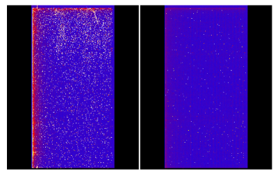
In the case of the CCD instrument aboard Hitomi (similarly named as SXI [8]), an aluminum optical blocking layer (OBL) was deposited on the surface of the CCDs. The instrument was, however, suffering from significant light leakages. The phenomenon was observed only during a specific time when the back side of the satellite was toward the day earth (MZDYE [5]). The main light path is presumed to be holes provided for other instruments in the base panel of the spacecraft, which indicates that the origin of light leakages is the Earth’s albedo i.e., reflection of the sunlight from the Earth. The obtained false signals are categorized into two types according to their event positions: point-like events (pinholes) scattered across the imaging area and end-surface leakage seen only near the edges of the chips. The left panel of figure 1 reproduces the MZDYE light leakages by a ground test with a FM spare CCD for Hitomi.
2.2 Improvement for XRISM
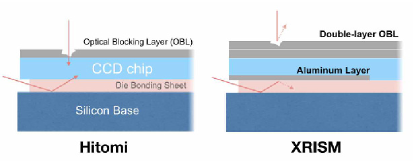
While XRISM is designed to close the holes that were the main cause of the problem, we further introduced a fail-safe design so that the CCD instrument itself can minimize the effect of light leakages. We took measures ensuring that additional design changes can resolve the above two problems. Below we summarize the causes of each type of light leakages and detailed design modifications of the XRISM SXI CCDs. Figure 2 indicates a schematic view of the new design for a XRISM CCD in comparison to that of Hitomi.
2.2.1 Pinholes
The origin of “pinholes” is voids generated in the aluminum OBL deposited on the Hitomi CCDs with a thickness of 100 nm. According to a Transmission Electron Microscope image of the OBL, the typical size of these voids is 1 m, which is much smaller than the pixel size of the CCD (). When visible light passing through the voids is scattered in the silicon dioxide layer between the OBL and silicon substrate, false signals are generated as a single- or multi-pixel event at each position under the pinholes and its surroundings (within pixels at a maximum). A similar phenomenon is reported on a ground-base test of CCDs for Origins, Spectral Interpretation, Resource Identification, Security, Regolith Explorer (OSIRIS-REx [9, 10]). They indicate that it is possibly due to particles or surface irregularities of the silicon substrate under the aluminum layer.
In our case, the main cause of the voids is considered to be a deterioration of the OBL due to a resist stripper used before aluminum vapor deposition. A follow-up test revealed that changing the type of the resist stripper can significantly reduce the number of pinholes. However, even with this change a slight increase of the number of pinholes over year was observed. We therefore introduced a double-layer aluminum deposition with a thickness of , so as to decrease the probability of pinhole formation on the OBL (figure 2). Although a reduced quantum efficiency in the soft X-ray band is a trade-off, we confirmed that it still satisfies the requirement of XRISM SXI. Note that the double-layer design has also been applied for the light filter of a PNCCD detector aboard extended Roentgen survey with an imaging telescope array (eROSITA [11, 12, 13, 14]) launched in July 2019, and no impact on in-orbit data has been reported.
2.2.2 End-surface Leakage
The “end-surface leakage” is another problem that we found in the Hitomi data. Significant light leakages were seen near the field of view of the SXI during MZDYE, which seems similar to that reported by Tsunemi et al. [15] in day-time data of MAXI/SSC. They speculate that the light entered through the edge of the MAXI CCD, whereas in our case the boundary around the imaging area of the Hitomi CCD has a dummy pixel region with a width of , that is larger than the attenuation length of visible light from the Sun. We thus conclude that the Hitomi CCD has another light path and that a sidewall coating of a silicon layer (e.g., [10]) is less effective for our case.
As shown in figure 2, the lateral structure of the SXI hints at the true origin of the end-surface leakage. In the design of the Hitomi CCD, a transparent die bonding sheet was used to adhere the silicon substrate and a silicon base. It was possible for the light scattered in the sheet to enter the imaging area. Similar cases are reported by (Bautz et al. [16] and Ryu et al. [10]) as backside leakage. To block the entering light, we additionally formed an aluminum filter on the backside electrode (under the passivation) layer of the XRISM CCDs with a width of 2 mm from the edge of the silicon substrate. The width of the filter is enough longer than the attenuation length of the scattered light, and because its parasitic capacitance is small enough to ignore, it does not affect the charge transfer performance of the CCDs as well.
3 Performance Test
We evaluate an optical blocking performance of the new CCD with a test sample that has the same design as the FM for XRISM. The CCD was cooled to C and illuminated with a monochromatic light using a light emitting diode (LED). The wavelength was set to nm, which is near the peak wavelength of the sunlight. Note that in this experiment we also simultaneously irradiated the CCD with X-rays from an 55Fe source for the purpose of calibration.
The right panel of Figure 1 shows a CCD image under the illumination of the above LED obtained with the test sample. The LED flash duration was 0.1 s for a single frame. For comparison, we also display an image obtained with a Hitomi FM spare CCD under the same condition in the left panel. It has a large number of pinholes and also the end-surface leakage with an irregular pattern originating from wrinkles of the die bonding sheet. These features are the same as those taken with Hitomi, indicating that our ground test reproduces the in-orbit light environment. The XRISM CCD image shows, on the other hand, a significant reduce both of the number of pinholes and the end-surface leakage region. The results demonstrate a substantial improvement of the optical blocking performance.
4 Analysis and Results
To give a quantitative evaluation of the optical blocking performance of the XRISM CCD, here we define a transmission factor (optical transmission) at a pixel position (X, Y) as
| (1) |
where and are the illuminance of light collected by the pixel and that at the OBL surface.
Given the luminous intensity of the LED is 10 mcd from a specification sheet, we can estimate the value of as follows:
| (2) |
where and are the distance from the LED to the CCD and the so-called utilization factor, respectively. While an accurate value of depends on the room index and reflectance of the camera chamber, we approximately set . Since the reflectance of inner walls of the aluminum chamber is roughly close to 90%, our calculation may be an underestimation on . Also, the LED has a slight directivity, which may give a larger . These factors result in that the following evaluation of is given under the most strict condition; smaller in reality would be expected than the calculation below.
Since 1 lx at corresponds to , the radiant flux and the integrated luminous energy absorbed per pixel are estimated as
| (3) |
where and are the size of a binned pixel and the duration time of the LED illumination, respectively. Thus, the expected increase of a pulse height amplitude (hereafter, “light leakages”) in analog-to-digital unit (ADU) can be represented as a function of the photon energy (eV) at a wavelength of (nm) and the CCD gain :
| (4) |
where is an offset due to fluctuations of the dark level between the LED-on and -off data: a few ADU in our experiment. The photon energy is fixed at and the gain .
Consequently, if the 0.1-s illumination results in an increase of , the transmission factor can be calculated as
| (5) |
From equation (5), if an increase of is caused by a 1-s illumination at (X, Y), the pixel has a transmission factor .
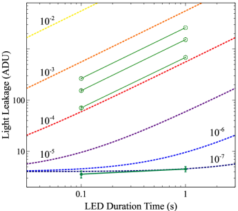
4.1 Pinholes
From mission requirements for the XRISM SXI, the number of pinhole pixels should be reduced less than 1.8% of all. The definition of the “pinhole pixels” given by the XRISM team is those whose transmission factor is . For instance, from equation (5), an equivalent threshold with the definition is for a 1-s illumination.
To measure for each pixel in the test sample CCD, we irradiated it with the LED light for various durations (0, 0.1, and 1 s). Increases of at each pixel were measured by subtracting the average pulse height from LED-on data () to that of LED off (). In the left panel of figure 3, we plot obtained values of light leakages at several example pinhole pixels and that of the surrounding normal region. The result indicates that the pinhole pixels significantly exceed the threshold transmission , whereas the normal region entirely satisfies the requirement.
The number ratio of the pinhole pixels is 0.2% () in the analyzed area. Since pinhole affected pixels tend to cluster within a few pixels, the real number of pinholes would be less than 0.1%. In the same way we calculated of the Hitomi FM CCD as 4.1% (). We therefore conclude that light leakages originated from pinholes were addressed by the double-layer OBL.
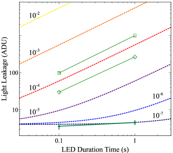
4.2 End-surface Leakage
It is requested for the XRISM mission to suppress the end-surface leakage up to at 3 pixels inward from the edge. The right panel of figure 3 indicates the average values of light leakages measured at the outermost edge () and that at 3 pixels inward (). Although the illuminance at the end-surface pixel should be somewhat different from , it can still be concluded that almost all inward pixels () are well below the threshold.
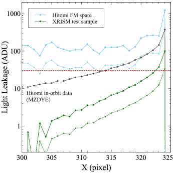
The left panel of figure 4 shows comparison between a profile of average near the edge of the test sample and that of the Hitomi FM spare CCD. The end-surface leakage at the outermost column is measured to be and 1231 ADU for XRISM and Hitomi, respectively. The result indicates a significant improvement on the end-surface leakage roughly by an order of magnitude with the new design.
In the same figure, we also plot the result of Hitomi taken during MZDYE, in which the value of light leakages is ADU at the edge. Given that the Hitomi FM and its spare CCDs have the same optical blocking performance, the result implies that our ground test is in more luminous environment than Hitomi in orbit, although the configuration (i.e., ) of the camera chamber is different between the ground test system and the Hitomi SXI. If this is the case, the end-surface leakage of the XRISM CCD is almost ignorable even at the outermost edge (the dotted line in figure 4).
| Numbering | Ratio of Pinholes | SXI Name | |
|---|---|---|---|
| segment AB | segment CD | ||
| FM02-01 | 0.06% | 0.04% | — |
| FM02-02 | 0.03% | 0.04% | CCD2 |
| FM02-03 | 0.05% | 0.03% | — |
| FM02-05 | 0.27% | 0.17% | — |
| FM02-06 | 0.17% | 0.30% | — |
| FM02-07 | 0.21% | 0.16% | — |
| FM02-08 | 0.21% | 0.28% | — |
| FM02-09 | 0.05% | 0.03% | CCD3 |
| FM02-10 | 0.06% | 0.04% | CCD1 |
| FM02-11 | 0.06% | 0.04% | — |
| FM02-12 | 0.02% | 0.03% | — |
| FM02-13 | 0.02% | 0.03% | CCD4 |
5 Optical Blocking Performance of FM CCDs
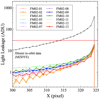
Since we confirmed that the new design is effective for suppression of both types of light leakages, we evaluated the optical blocking performance of twelve FM CCDs in a screening test. In the following analysis, we estimated in-orbit values of light leakages by correcting an expected illuminance based on comparison of the end-surface leakage at the outermost column between the screening test and the Hitomi MZDYE.
The results for the pinholes and the end-surface leakage are summarized in table 1 and in the right panel of figure 4, respectively. The ratios of pinholes for each CCD show that all the CCDs except several segments satisfy the requirement, which will remain unchanged by the end of life of XRISM, even taking into account a possible increase of the pinholes. As shown in figure 4, we also confirmed that all the pulse height profiles of the FM CCDs are below the given threshold. The plot indicates that the end-surface leakage as well satisfies the requirement.
We thus conclude that the issues of light leakages found in the Hitomi data are totally solved by changing the optical blocking design and that the XRISM CCDs enough meet the mission requirement for the SXI. From these results, we selected best four CCDs to be installed in the SXI, also based on several criteria such as the energy resolution and charge transfer efficiency (Yoneyama et al. submitted to NIMA).
Acknowledgements
This work is supported by JSPS KAKENHI Grand Numbers JP19K03915 (H.U.), JP15H02090 (T.G.T.), JP20H01947 (H.N.), JP16H03983 (K.M.), JP18H01256 (H.N.), and JP17K14289 (M.N.).
References
- [1] Turner, M. J. L., Abbey, A., Arnaud, M., Balasini, M., et al., The european photon imaging camera on xmm-newton: The mos cameras, A&A 365 (1) (2001) L27–L35.
- [2] K. Koyama, H. Tsunemi, T. Dotani, M. W. Bautz, et al., X-Ray Imaging Spectrometer (XIS) on Board Suzaku, Publications of the Astronomical Society of Japan 59 (sp1) (2007) S23–S33.
- [3] T. Takahashi, M. Kokubun, K. Mitsuda, R. L. Kelley, et al., Hitomi (ASTRO-H) X-ray Astronomy Satellite, Journal of Astronomical Telescopes, Instruments, and Systems 4 (2018) 021402.
- [4] M. Barbera, G. Branduardi-Raymont, A. Collura, A. Comastri, et al., The optical blocking filter for the ATHENA wide field imager: ongoing activities towards the conceptual design, Vol. 9601 of Society of Photo-Optical Instrumentation Engineers (SPIE) Conference Series, 2015, p. 960109.
- [5] H. Nakajima, Y. Maeda, H. Uchida, T. Tanaka, et al., In-orbit performance of the soft X-ray imaging system aboard Hitomi (ASTRO-H), PASJ 70 (2) (2018) 21.
- [6] M. Tashiro, H. Maejima, K. Toda, R. Kelley, et al., Concept of the X-ray Astronomy Recovery Mission, Vol. 10699 of Society of Photo-Optical Instrumentation Engineers (SPIE) Conference Series, 2018, p. 1069922.
- [7] K. Hayashida, H. Tomida, K. Mori, H. Nakajima, et al., Soft x-ray imaging telescope (Xtend) onboard X-ray Astronomy Recovery Mission (XARM), Vol. 10699 of Society of Photo-Optical Instrumentation Engineers (SPIE) Conference Series, 2018, p. 1069923.
- [8] T. Tanaka, H. Uchida, H. Nakajima, H. Tsunemi, et al., Soft X-ray Imager aboard Hitomi (ASTRO-H), Journal of Astronomical Telescopes, Instruments, and Systems 4 (1) (2018) 1 – 15.
- [9] K. K. Ryu, B. E. Burke, H. R. Clark, et al., Development of CCDs for REXIS on OSIRIS-REx, in: Space Telescopes and Instrumentation 2014: Ultraviolet to Gamma Ray, Vol. 9144, International Society for Optics and Photonics, SPIE, 2014, pp. 1431 – 1438.
- [10] K. K. Ryu, M. W. Bautz, S. E. Kissel, P. O’Brien, V. Suntharalingam, Journal of Astronomical Telescopes, Instruments, and Systems 3 (3) (2017) 1 – 7.
- [11] N. Meidinger, R. Andritschke, J. Elbs, S. Granato, et al., Status of the CCD camera for the eROSITA space telescope, in: UV, X-Ray, and Gamma-Ray Space Instrumentation for Astronomy XVII, Vol. 8145, International Society for Optics and Photonics, SPIE, 2011, pp. 33 – 44.
- [12] N. Meidinger, R. Andritschke, F. Aschauer, J. Elbs, et al., Design and performance of the eROSITA focal plane instrumentation, in: High Energy, Optical, and Infrared Detectors for Astronomy V, Vol. 8453, International Society for Optics and Photonics, SPIE, 2012, pp. 191 – 201.
- [13] S. Granato, The response of silicon pnccd sensors with aluminium on-chip filter to visible light, uv- and x-ray radiation, Available at http://inis.iaea.org/search/search.aspx?orig_q=RN:44052575.
- [14] S. Granato, R. Andritschke, J. Elbs, N. Meidinger, et al., Characterization of erosita pnccds, IEEE Transactions on Nuclear Science 60 (4) (2013) 3150–3157.
- [15] H. Tsunemi, H. Tomida, H. Katayama, et al., In-Orbit Performance of the MAXI/SSC onboard the ISS, Publications of the Astronomical Society of Japan 62 (6) (2010) 1371–1379.
- [16] M. Bautz, S. Kissel, R. Masterson, K. Ryu, V. Suntharalingam, Directly-deposited blocking filters for high-performance silicon x-ray detectors, in: Space Telescopes and Instrumentation 2016: Ultraviolet to Gamma Ray, Vol. 9905, International Society for Optics and Photonics, SPIE, 2016, pp. 1384 – 1391.