Synthesis and Local Probe Gating of a Monolayer Metal-Organic Framework
Abstract
Achieving large-area uniform two-dimensional (2D) metal-organic frameworks (MOFs) and controlling their electronic properties on inert surfaces is a big step towards future applications in electronic devices. Here we successfully fabricated a 2D monolayer Cu-dicyanoanthracene (DCA) MOF with long-range order on an epitaxial graphene surface. Its structural and electronic properties are studied by low-temperature scanning tunneling microscopy (STM) and spectroscopy (STS) complemented by density-functional theory (DFT) calculations. We demonstrate access to multiple molecular charge states in the 2D MOF using tip-induced local electric fields. We expect that a similar strategy could be applied to fabricate and characterize 2D MOFs with exotic, engineered electronic states.
1 Introduction
Metal-organic frameworks (MOFs) are an important class of materials that have been intensively studied in the last two decades. Despite the vast number of reports on three-dimensional, bulk MOFs, synthesis and characterization of two-dimensional (2D), single layer MOFs are much more limited Kambe et al. (2013); Gao et al. (2019); Zhang et al. (2020). Intrinsic 2D MOFs are expected to attract increasing attention since they are anticipated to possess exotic electronic properties, such as high electrical conductivity Sheberla et al. (2014); Kambe et al. (2014); Huang et al. (2015); Chen et al. (2018); Xie et al. (2020), superconductivity Zhang et al. (2017); Huang et al. (2018), topologically non-trivial band structure Wang et al. (2013); Jiang and Liu (2017); Crasto De Lima et al. (2019); Zhang et al. (2019); Jiang et al. (2020); Silveira et al. (2020); Gao et al. (2020), half-metallic ferromagnetism Zhao et al. (2013); Zhang and Zhao (2015); Jin et al. (2018); Zhang et al. (2019) and quantum spin liquids Yamada et al. (2017). To isolate their intrinsic electronic properties from the substrate, synthesis of 2D MOFs on inert surfaces, such as graphene, other van der Waals layered materials, and bulk insulators, is highly desired. Furthermore, understanding the performance of 2D MOFs in a gated device at the atomic scale would be essential for future applications.
On-surface 2D porous metal-organic networks, which represent a 2D analogue of 3D MOFs, have been fabricated following the concepts of supramolecular coordination chemistry Lin et al. (2009); Barth (2009). By tuning the selection of metal atoms and organic linkers, different kinds of lattice structures of 2D MOFs can be fabricated Dong et al. (2016). Since the symmetry of the band structure is controlled by the lattice structure, it is expected that specific electronic properties can be realized in certain MOF geometries. However, there are very few reports on 2D MOFs on inert surfaces, where the MOF would retain its intrinsic electronic properties. More crucially, existing work only demonstrates order on a local scale with very small domain sizes of the MOF Kambe et al. (2013); Urgel et al. (2015); Schüller et al. (2016); Kumar et al. (2018); Zhao et al. (2019); Li et al. (2019). The characterization of single layer MOFs in a gated device environment has not been realized yet, since it is even more challenging to fabricate 2D MOFs on a three-terminal device. However, this could be alternatively achieved by gating the 2D MOFs using local electric fields induced by the tip of a scanning probe microscope.
In this work, we successfully fabricated 2D monolayer Cu-dicyanoanthracene (DCA) MOF on an epitaxial graphene surface under ultra-high vacuum (UHV) conditions by precisely controlling the growth parameters. Its structural and electronic properties are studied by low-temperature scanning tunneling microscopy (STM) and spectroscopy (STS) complemented by density-functional theory (DFT) calculations. The ordered DCA3Cu2 network shows a structure combining a honeycomb lattice of Cu atoms with a kagome lattice of DCA molecules and is predicted to be a 2D topological insulator Zhang et al. (2016). Notably, we demonstrate very long-range order of the DCA-Cu MOF and show that it can grow across the step-edges of the underlying substrate. This facilitates the synthesis of uniform, single-crystalline monolayer MOFs. Combing the STM/STS data with DFT results, we confirm that a kagome band structure is formed in the 2D MOF near the Fermi level. Interestingly, we found that multiple molecular charge states can be generated and modified through the tip-induced local electric fields.
2 Results and Discussion
We deposit DCA molecules and Cu atoms sequentially onto the graphene (G/Ir(111)) substrate held at room temperature (details given in the Experimental Section). By tuning the DCA:Cu ratio, both the DCA3Cu single complex (Figures S1 and S11) and the DCA3Cu2 honeycomb network can be fabricated. The initial sample quality can be improved by annealing the sample at 50 ∘C. This helps to grow larger DCA3Cu2 networks up to a full monolayer, as shown in Figures 1 and S2a. The proper annealing temperature is vital for the formation of a uniform monolayer 2D MOF, since the coordination bonds are relatively weak and reversible Shi et al. (2011); Cai et al. (2017). The networks are structurally robust, which is evidenced by the fact that they grow seamlessly across step edges of the underlying Ir(111) substrate (see Figure 1b). Annealing at a higher temperature (C) yields a new phase of close-packed DCA molecules and large Cu islands (see Figure S2b).
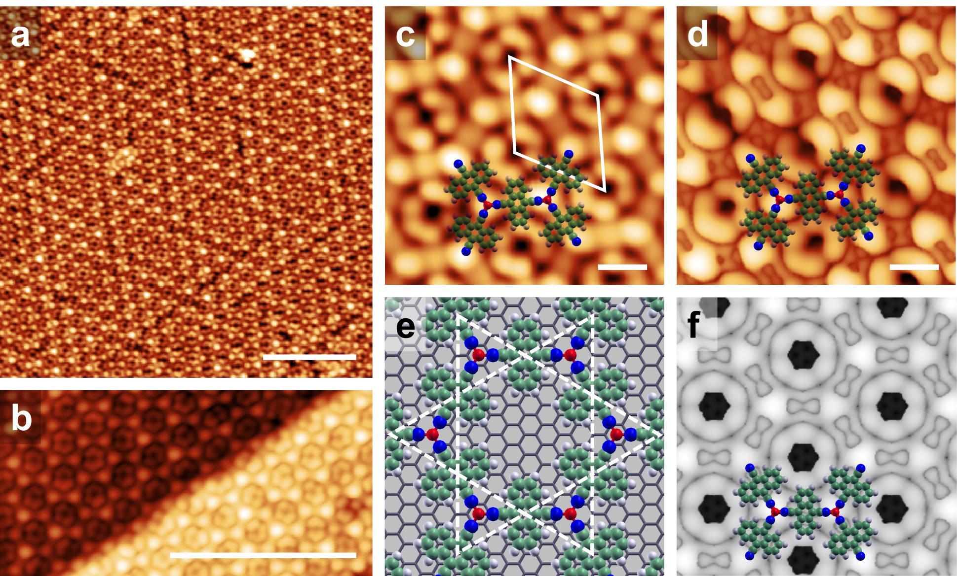
Figure 1c shows a high-resolution image of the backbone of DCA3Cu2 network, with the unit cell shown as a white parallelogram with a lattice constant of nm, which is consistent with the DFT value of 1.98 nm and in the range of previous reports of the network on a Cu(111) surface Pawin et al. (2008); Zhang et al. (2014). While the Cu atoms arrange in a honeycomb lattice in the network, the DCA molecules form a kagome pattern, as shown in the model of Figure 1e. Figure 1d shows the same area at a bias voltage corresponding to the low energy electronic band of the Cu-DCA network (see below for more detailed spectroscopy of the Cu-DCA network electronic structure). The image is acquired with a molecule-modified tip apex, which enhances the spatial resolution of the local density of states (LDOS) Repp et al. (2005). The experimental image is nicely reproduced by the STM image simulations based on density-functional theory (DFT) calculations of the Cu-DCA structure shown in Figure 1f (see below for details). The modest contrast difference between the DCA molecules in Figure 1d is caused by the Moiré pattern of graphene on Ir(111) (cf. Supporting Information, Figure S3).
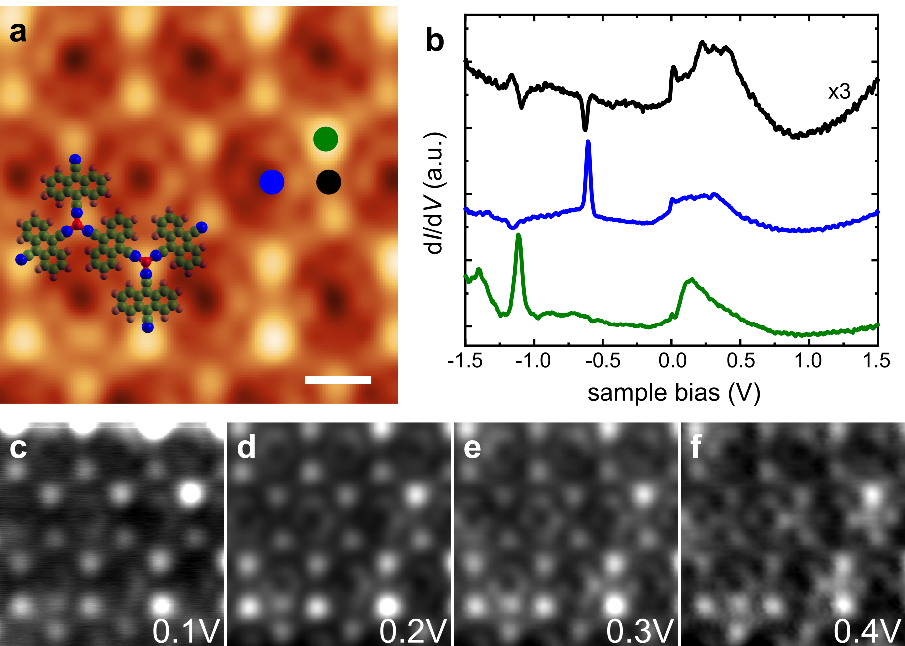
Figure 2 shows the d/d spectra recorded on different high symmetry sites of the network. All the spectra in Figure 2b exhibit a broad peak in the energy range between 0 V to 0.5 V. The contrast in constant height d/d maps in Figure 2c is not strongly bias dependent in the range from 0.1 V to 0.4 V and reproduced well by the DFT simulations (Figure S9). We attribute these features to the band structure formed in the 2D network, which has been well studied in similar DCA3Co2 network Kumar et al. (2018) and will be explored in more detail in Figure 3. Interestingly, the STS measured on the center of the DCA molecule (black curve in Figure 2b) shows two sharp dips around -0.6 V and -1.2 V; the STS on top of the Cu atom (green curve in Figure 2b) shows a small dip around -0.6 V and a sharp peak around -1.2 V; the end of the long axis of the DCA molecule (blue curve in Figure 2b) shows a sharp peak around -0.6 V and a tiny dip around -1.2 V. The peaks/dips at these two bias values are attributed to the typical charging features, where the charge state of the molecule under the tip changes due to the tip-induced local electric field Wu et al. (2004); Nazin et al. (2005); Pradhan et al. (2005); Nazin et al. (2005); Fernández-Torrente et al. (2012); Schulz et al. (2013, 2015); Liu et al. (2015); Wickenburg et al. (2016); Kocić et al. (2019); Kumar et al. (2019); Pham et al. (2019); Pörtner et al. (2020). We will discuss the details of these charging features in Figure 4. The spectra of the MOF on the step edge of the underlying Ir(111) substrate (Figure S12) is consistent with the one on the flat area (Figure 2), indicating that the electronic properties of the MOF are effectively decoupled from the metal substrate by the graphene layer. Besides, all the spectra show a small and sharp peak at or very close to the Fermi level (0-10 mV), which we attribute as a charging peak as well (cf. Supporting Information, Figure S4).
The DFT simulated band structure of the gas-phase DCA3Cu2 network (Figure 3a) shows a kagome band structure around Fermi level which consists of a Dirac band with an additional flat band pinned to the top of the Dirac band Leykam et al. (2018); Yan and Liljeroth (2019); Jing and Heine (2019). The band structure of the DCA3Cu2 network on graphene (the MOF states represented in purple in Figure 3b) shows very similar features with an additional avoided crossing between the MOF kagome and the graphene Dirac bands due to weak hybridization between them. While the Dirac points of the isolated DCA3Cu2 network and graphene are both located at the Fermi level in the gas phase, the Dirac point in the DCA3Cu2 kagome band on graphene is 0.3 eV above the Dirac point of the graphene substrate, indicating a charge transfer between the DCA3Cu2 network and the graphene substrate (cf. Figure S7). This is consistent with the experimental finding that the energy levels of the DCA3Cu2 kagome band are mostly above the Fermi level. Note that in a clean G/Ir(111) sample, the Dirac point of graphene is 100 meV above the Fermi level as well Pletikosić et al. (2009). However, the experimental d/d spectra did not resolve the bandgap of the MOF at the Dirac point. This is mainly due to a certain lifetime broadening and the satellite vibrionic peaks coming from the intermolecular electronic coupling which broadens the spectra.
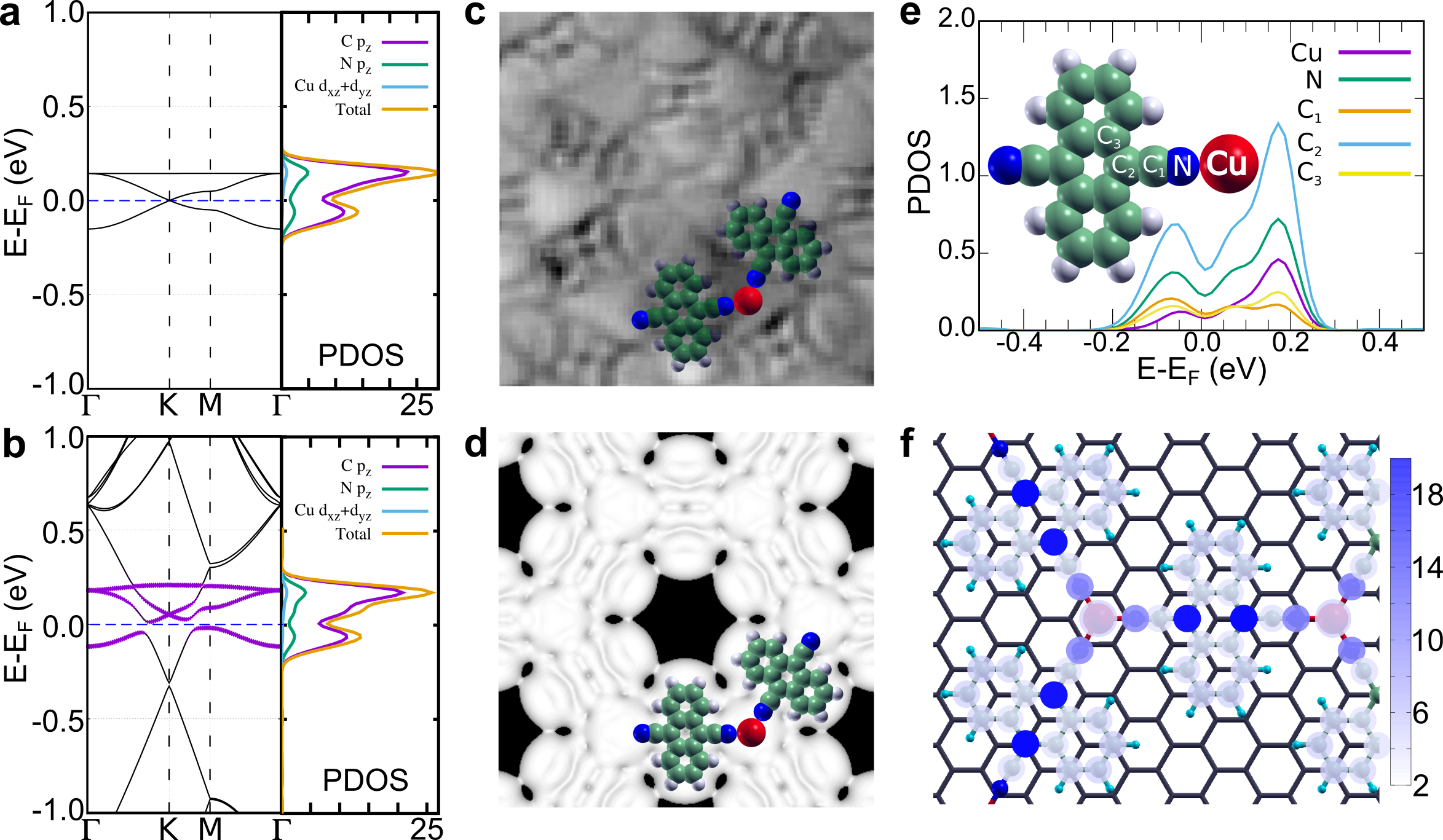
The projected density of states (PDOS) in Figure 3 show that the kagome band originates mainly from the DCA molecule ( orbitals of C and N atoms), with very minor contributions from the Cu orbitals (+), indicating that the kagome geometry of the DCA molecular array and the - extended conjugation in the metal-organic framework is realized in this band structure Sheberla et al. (2014); Huang et al. (2015); Dou et al. (2017); Day et al. (2019); Xie et al. (2020). The DFT simulated LDOS maps show uniform features at different energies within the kagome band (Figures S5a-d). To probe the electronic structure of the DCA3Cu2 network in more detail, we used a molecule-modified -wave tip to get the high-resolution LDOS maps Gross et al. (2011) shown in Figures S5e-h. These show homogeneous appearances which are similar at different biases as in the simulated results. The representative experimental and DFT simulated LDOS maps are shown in Figures 3c and 3d, respectively. The experimental maps match the representative DFT simulated data very well. The minor contrast difference comes from the moiré pattern and slight inhomogeneities of the graphene substrate, which is also reflected in the charging rings shown in Figure 4.
Charging behavior has been studied in detail in the case of single molecules or self-assembled molecular monolayers on coinage metal surfaces such as Au(111) Fernández-Torrente et al. (2012) and Ag(111) Kocić et al. (2019); Kumar et al. (2019) and more frequently found when the molecule is decoupled from the substrate by an ultra-thin film such as Al2O3 Wu et al. (2004); Nazin et al. (2005); Pradhan et al. (2005); Nazin et al. (2005), graphene Wickenburg et al. (2016); Pham et al. (2019) and hexagonal boron nitride Schulz et al. (2013, 2015); Liu et al. (2015); Pörtner et al. (2020). It can be explained by considering the tip-molecule-substrate system as a double-barrier tunnel junction (DBTJ) as illustrated in Figures 4a and 4b. When a bias voltage is applied across the DBTJ, there is a potential distribution with a drop at both the tip-molecule and the molecule-substrate junctions. Consequently, applying a bias voltage causes the molecular levels to shift in energy by , where is the fraction of the potential drop between the molecule and the substrate with respect to the overall bias. If there are molecular energy levels close to the Fermi level, these can shift across it at some value of the bias voltage and the charge state of the molecule changes by . In our particular case, the charging occurs once the band bottom of the kagome band (KB) shifts down below the Fermi level: . The charging features can be distinguished from the usual molecular resonances by checking how the charging peak/dip shifts as a function of the tip-molecule distance. Bringing the tip closer to the molecule reduces and, consequently, the charging features shift towards the Fermi level monotonously with decreasing tip-molecule distance (shown in Figure 4c), which is consistent with previous studies Wu et al. (2004); Pham et al. (2019); Kumar et al. (2019). The charging features shift by about 8.8 mV/Å upon reducing the tip-sample distance approach. On the other hand, the kagome band position at the positive bias barely changes with different tip-molecule distances, which can also be seen from Figure 4c.
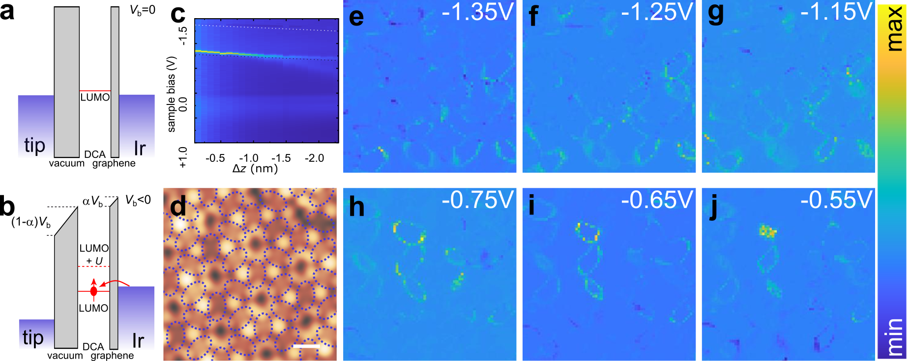
Another fingerprint of a charging phenomenon is the charging ring feature. As shown in Figures 4d-4j, the elliptical rings observed in the LDOS maps at different bias voltages represent the onset of charging as the tip is moved towards the charging site. Notably, in the previous experiments, both the charging peaks Nazin et al. (2005); Pradhan et al. (2005); Nazin et al. (2005); Wickenburg et al. (2016); Pham et al. (2019) and dips Fernández-Torrente et al. (2012); Kocić et al. (2019); Kumar et al. (2019) have been found at negative bias. The presence of a peak or dip in the d/d spectrum depends on whether the LDOS at the tip position increases or decreases due to the charging event, which might also depend on the local adsorption registry between the MOF and the underlying graphene substrate. The charging peak/dip rings features around two different bias voltages: one around -1.2 V (Figures 4e-4g) and the other -0.6 V (Figures 4h-4j). The energy difference of the two charging rings reflects the Coulomb charging energy ( 0.6 eV). The peak and dip features can either coexist around a specific molecule or one of them can be dominant. Around both biases, the charging ring perimeter decreases as the bias becomes less negative, which is also consistent with the previous works. Figure 4d highlights all the possible charging rings with dotted purple ellipses. However, the charging ring positions and perimeters in the experimental data are not entirely identical (Figures 4e-4j). Each molecule has slightly varying adsorption environment (e.g. due to the moiré pattern on graphene on Ir(111) which is known to give rise to a work function modulation of a couple of hundred meV Craes et al. (2013); Järvinen et al. (2014); Altenburg and Berndt (2014); Kumar et al. (2017)), varying the exact on-set bias of the charging Fernández-Torrente et al. (2012); Liu et al. (2015); Kumar et al. (2019); Pörtner et al. (2020). The elliptical rings are mostly around the DCA molecules, which is consistent with the DFT results that the band above the Fermi level (which is pulled below at negative bias) has most of its density on the DCA molecules. These local charging features demonstrate that electron-electron interactions (characterized by the Coulomb charging energy, here 0.6 eV) are significant and they can be expected to be of a similar magnitude compared to the overall band width of the Cu-DCA network (here several hundreds of meV.)). Cu-DCA has been predicted to be an intrinsic 2D topological insulator in a non-interacting model Zhang et al. (2016), but our results indicate the need to go beyond this simple picture and consider electron-electron interactions.
3 Conclusion
In summary, we study the structural and electronic properties of monolayer Cu-DCA MOF on a G/Ir(111) substrate under UHV conditions using experimental (STM/STS) and theoretical (DFT) methods. We demonstrate successful synthesis of a large-scale monolayer MOF that can grow across the terrace of the graphene substrate. The 2D Cu-DCA MOF possesses a kagome band structure near the Fermi level. We expect that a similar strategy could be applied to fabricate and characterize 2D MOFs with exotic electronic states on weakly interacting substrates, e.g. 2D MOFs with heavy metal atoms Shi and Lin (2009); Lyu et al. (2015); Sun et al. (2016); Song et al. (2017); Yang et al. (2018); Yan et al. (2018); Sun et al. (2018); Yan et al. (2019) possessing strong spin-orbit couplings and the possibility of realizing an organic topological insulator Springer et al. (2020). In addition, multiple molecular charge states are observed and modified by the tip-induced local electric fields. This highlights the role of electron-electron interactions that are likely to be of a similar order of magnitude as the overall band width. Depending on the relative magnitudes of the different energy scales, this can give rise to magnetically ordered or spin liquid ground states or – when coupled with spin-orbit interactions – result in a quantum anomalous Hall insulator or more exotic electronic states. Raghu et al. (2008); Pesin and Balents (2010); Ren et al. (2016); Rachel (2018).
Methods
Sample preparation and STM experiments were carried out in an ultrahigh vacuum system with a base pressure of mbar. The Ir(111) single crystal sample was cleaned by repeated cycles of Ne+ sputtering at 2 kV and annealing in an oxygen environment at 900 ∘C followed by flashing to 1300 ∘C. Graphene was grown by adsorbing ethylene and flashing the sample to 1100 - 1300 ∘C in a TPG (temperature programmed growth) step followed by a CVD step where the Ir(111) substrate at 1100 - 1300 ∘C is exposed to ethylene gas at mbar pressure for 1 minute Coraux et al. (2009). This gives approximately a full monolayer coverage of graphene (G/Ir(111)).
The DCA3Cu single complex and DCA3Cu2 network can be fabricated by the sequential deposition of 9,10-dicyanoanthracene (DCA, Sigma Aldrich) molecules and Cu atoms onto the G/Ir(111) substrate held at room temperature. Further annealing the sample at 50 ∘C results in DCA3Cu2 network growth until monolayer coverage is reached. DCA molecules were thermally evaporated from a resistively heated aluminum oxide crucible at 100 ∘C. Subsequently, the samples were inserted into a low-temperature STM (Createc GmbH), and all subsequent experiments were performed at K. STM images were taken in the constant current mode. d/d spectra were recorded by standard lock-in detection while sweeping the sample bias in an open feedback loop configuration, with a peak-to-peak bias modulation of 15 - 20 mV at a frequency of 526 Hz. In the local density of states (LDOS) maps, each d/d spectrum was normalized by spectra to minimize the height difference contribution Stroscio et al. (1986); Klappenberger et al. (2011). The STM images were processed by Gwyddion software Nečas and Klapetek (2012).
The DFT calculations were performed with the QUANTUM-ESPRESSO distribution Giannozzi et al. (2009). We used the optB86b-vdW functional Klimeš et al. (2011); Dion et al. (2004) to optimize the structure of the DCA3Cu2 MOF both as an isolated layer and on graphene. To describe the interaction between electrons and ions we used PAW pseudopotentials Blöchl (1994), while the electronic wave functions were expanded considering a plane-wave basis set with kinetic energy cutoffs of 90 Ry. Integrations over the Brillouin zone (BZ) were performed using a uniform grid of -points, and a twice denser grid was used to obtain band structures and PDOS. The electronic structure for the STM simulations and LDOS maps were calculated via FHI-AIMS package Blum et al. (2009) from the previously optimized geometry as a single point calculation. For this calculations we made use of the Perdew-Burke-Ernzerhof (PBE) exchange-correlation functional Perdew et al. (1996) with -point only. The s and pxy wave STM simulations and LDOS maps were then computed by means of the PP-STM code with fixed tip, where the broadening parameter was set to 0.3 eV Krejčí et al. (2017). The fixed tip simulations fingerprint only the electronic structure of the sample in the following manner: The s-tip d/d signal is given by: , while the pxy-tip dI/dV signal can be calculated as: Gross et al. (2011); Krejčí et al. (2017). The normalized LDOS maps have been simulated via plotting iso-surface of the corresponding d/d signal.
Supporting Information
Supporting Information is available.
Acknowledgments
This research made use of the Aalto Nanomicroscopy Center (Aalto NMC) facilities. We acknowledge support from the European Research Council (ERC-2017-AdG no. 788185 “Artificial Designer Materials”) and Academy of Finland (Academy projects no. 311012 and 314882, and Academy professor funding no. 318995 and 320555). Linghao Yan and Ondřej Krejčí acknowledge support from European Union’s Horizon 2020 research and innovation program (Marie Skłodowska-Curie Actions Individual Fellowship no. 839242 “EMOF” and no. 845060 “QMKPFM”). Computing resources from the Aalto Science-IT project and CSC, Helsinki are gratefully acknowledged. ASF has been supported by the World Premier International Research Center Initiative (WPI), MEXT, Japan.
References
- Kambe et al. (2013) T. Kambe, R. Sakamoto, K. Hoshiko, K. Takada, M. Miyachi, J.-H. Ryu, S. Sasaki, J. Kim, K. Nakazato, M. Takata, H. Nishihara, J. Am. Chem. Soc 2013, 135, 2462.
- Gao et al. (2019) Z. Gao, C. H. Hsu, J. Liu, F. C. Chuang, R. Zhang, B. Xia, H. Xu, L. Huang, Q. Jin, P. N. Liu, N. Lin, Nanoscale 2019, 11, 878.
- Zhang et al. (2020) R. Zhang, J. Liu, Y. Gao, M. Hua, B. Xia, P. Knecht, A. C. Papageorgiou, J. Reichert, J. V. Barth, H. Xu, L. Huang, N. Lin, Angew. Chemie Int. Ed. 2020, 59, 2669.
- Sheberla et al. (2014) D. Sheberla, L. Sun, M. A. Blood-Forsythe, S. Er, C. R. Wade, C. K. Brozek, A. Aspuru-Guzik, M. Dincǎ, J. Am. Chem. Soc 2014, 136, 8859.
- Kambe et al. (2014) T. Kambe, R. Sakamoto, T. Kusamoto, T. Pal, N. Fukui, K. Hoshiko, T. Shimojima, Z. Wang, T. Hirahara, K. Ishizaka, S. Hasegawa, F. Liu, H. Nishihara, J. Am. Chem. Soc 2014, 136, 14357.
- Huang et al. (2015) X. Huang, P. Sheng, Z. Tu, F. Zhang, J. Wang, H. Geng, Y. Zou, C.-a. Di, Y. Yi, Y. Sun, W. Xu, D. Zhu, Nat. Commun. 2015, 6, 7408.
- Chen et al. (2018) I.-F. Chen, C.-F. Lu, W.-F. Su, Langmuir 2018, 34, 15754.
- Xie et al. (2020) L. S. Xie, G. Skorupskii, M. Dincă, Chem. Rev. 2020, 8536.
- Zhang et al. (2017) X. Zhang, Y. Zhou, B. Cui, M. Zhao, F. Liu, Nano Lett. 2017, 17, 6166.
- Huang et al. (2018) X. Huang, S. Zhang, L. Liu, L. Yu, G. Chen, W. Xu, D. Zhu, Angew. Chem. Int. Ed. 2018, 57, 146.
- Wang et al. (2013) Z. Wang, Z. Liu, F. Liu, Nat. Commun. 2013, 4, 1471.
- Jiang and Liu (2017) W. Jiang, F. Liu in World Scientific Reference on Spin in Organics, Vol. 2, World Scientific, 2017, Chapter 6, pp. 201–224.
- Crasto De Lima et al. (2019) F. Crasto De Lima, G. J. Ferreira, R. H. Miwa, J. Chem. Phys. 2019, 150, 234701.
- Zhang et al. (2019) J. Zhang, B. Zhao, C. Ma, Z. Yang, Appl. Phys. Lett. 2019, 114, 043102.
- Jiang et al. (2020) W. Jiang, S. Zhang, Z. Wang, F. Liu, T. Low, Nano Lett. 2020, 20, 1959.
- Silveira et al. (2020) O. J. Silveira, G. A. S. Ribeiro, H. Chacham, Appl. Phys. Lett. 2020, 116, 103103.
- Gao et al. (2020) Y. Gao, Y.-Y. Zhang, J.-T. Sun, L. Zhang, S. Zhang, S. Du, Nano Res. 2020, 13, 1571.
- Zhao et al. (2013) M. Zhao, A. Wang, X. Zhang, Nanoscale 2013, 5, 10404.
- Zhang and Zhao (2015) X. Zhang, M. Zhao, Sci. Rep. 2015, 5, 14098.
- Jin et al. (2018) Y. Jin, Z. Chen, B. Xia, Y. Zhao, R. Wang, H. Xu, Phys. Rev. B 2018, 98, 245127.
- Zhang et al. (2019) L. C. Zhang, L. Zhang, G. Qin, Q. R. Zheng, M. Hu, Q. B. Yan, G. Su, Chem. Sci. 2019, 10, 10381.
- Yamada et al. (2017) M. G. Yamada, H. Fujita, M. Oshikawa, Phys. Rev. Lett. 2017, 119, 057202.
- Lin et al. (2009) N. Lin, S. Stepanow, M. Ruben, J. V. Barth, Top. Curr. Chem. 2009, 287, 1.
- Barth (2009) J. V. Barth, Surf. Sci. 2009, 603, 1533.
- Dong et al. (2016) L. Dong, Z. Gao, N. Lin, Prog. Surf. Sci. 2016, 91, 101.
- Urgel et al. (2015) J. Urgel, M. Schwarz, M. Garnica, D. Stassen, D. Bonifazi, D. Ecija, J. Barth, W. Auwärter, J. Am. Chem. Soc. 2015, 137, 2420.
- Schüller et al. (2016) L. Schüller, V. Haapasilta, S. Kuhn, H. Pinto, R. Bechstein, A. S. Foster, A. Kühnle, J. Phys. Chem. C 2016, 120, 14730.
- Kumar et al. (2018) A. Kumar, K. Banerjee, A. S. Foster, P. Liljeroth, Nano Lett. 2018, 18, 5596.
- Zhao et al. (2019) Y. Zhao, B. Yuan, C. Li, P. Zhang, Y. Mai, D. Guan, Y. Li, H. Zheng, C. Liu, S. Wang, J. Jia, ChemPhysChem 2019, 20, 2394.
- Li et al. (2019) J. Li, L. Solianyk, N. Schmidt, B. Baker, S. Gottardi, J. C. Moreno Lopez, M. Enache, L. Monjas, R. Van Der Vlag, R. W. Havenith, A. K. Hirsch, M. Stöhr, J. Phys. Chem. C 2019, 123, 12730.
- Zhang et al. (2016) L. Z. Zhang, Z. F. Wang, B. Huang, B. Cui, Z. Wang, S. X. Du, H.-J. Gao, F. Liu, Nano Lett. 2016, 16, 2072.
- Shi et al. (2011) Z. Shi, J. Liu, T. Lin, F. Xia, P. N. Liu, N. Lin, J. Am. Chem. Soc 2011, 133, 6150.
- Cai et al. (2017) L. Cai, Q. Sun, M. Bao, H. Ma, C. Yuan, W. Xu, ACS Nano 2017, 11, 3727.
- Tersoff and Hamann (1985) J. Tersoff, D. R. Hamann, Phys. Rev. B 1985, 31, 805–813.
- Pawin et al. (2008) G. Pawin, K. Wong, D. Kim, D. Sun, L. Bartels, S. Hong, T. Rahman, R. Carp, M. Marsella, Angew. Chem. Int. Ed. 2008, 47, 8442.
- Zhang et al. (2014) J. Zhang, A. Shchyrba, S. Nowakowska, E. Meyer, T. A. Jung, M. Muntwiler, Chem. Commun. 2014, 50, 12289.
- Repp et al. (2005) J. Repp, G. Meyer, S. M. Stojković, A. Gourdon, C. Joachim, Phys. Rev. Lett. 2005, 94, 026803.
- Wu et al. (2004) S. W. Wu, G. V. Nazin, X. Chen, X. H. Qiu, W. Ho, Phys. Rev. Lett. 2004, 93, 236802.
- Nazin et al. (2005) G. V. Nazin, X. H. Qiu, W. Ho, J. Chem. Phys. 2005, 122, 181105.
- Pradhan et al. (2005) N. A. Pradhan, N. Liu, C. Silien, W. Ho, Phys. Rev. Lett. 2005, 94, 076801.
- Nazin et al. (2005) G. V. Nazin, X. H. Qiu, W. Ho, Phys. Rev. Lett. 2005, 95, 166103.
- Fernández-Torrente et al. (2012) I. Fernández-Torrente, D. Kreikemeyer-Lorenzo, A. Stróżecka, K. J. Franke, J. I. Pascual, Phys. Rev. Lett. 2012, 108, 036801.
- Schulz et al. (2013) F. Schulz, R. Drost, S. K. Hämäläinen, P. Liljeroth, ACS Nano 2013, 7, 11121.
- Schulz et al. (2015) F. Schulz, M. Ijäs, R. Drost, S. K. Hämäläinen, A. Harju, A. P. Seitsonen, P. Liljeroth, Nat. Phys. 2015, 11, 229.
- Liu et al. (2015) L. Liu, T. Dienel, R. Widmer, O. Gröning, ACS Nano 2015, 9, 10125.
- Wickenburg et al. (2016) S. Wickenburg, J. Lu, J. Lischner, H. Z. Tsai, A. A. Omrani, A. Riss, C. Karrasch, A. Bradley, H. S. Jung, R. Khajeh, D. Wong, K. Watanabe, T. Taniguchi, A. Zettl, A. H. Neto, S. G. Louie, M. F. Crommie, Nat. Commun. 2016, 7, 13553.
- Kocić et al. (2019) N. Kocić, D. Blank, P. Abufager, N. Lorente, S. Decurtins, S. X. Liu, J. Repp, Nano Lett. 2019, 19, 2750.
- Kumar et al. (2019) D. Kumar, C. Krull, Y. Yin, N. V. Medhekar, A. Schiffrin, ACS Nano 2019, 13, 11882.
- Pham et al. (2019) V. D. Pham, S. Ghosh, F. Joucken, M. Pelaez-Fernandez, V. Repain, C. Chacon, A. Bellec, Y. Girard, R. Sporken, S. Rousset, Y. J. Dappe, S. Narasimhan, J. Lagoute, npj 2D Mater. Appl. 2019, 3, 5.
- Pörtner et al. (2020) M. Pörtner, Y. Wei, A. Riss, K. Seufert, M. Garnica, J. V. Barth, A. P. Seitsonen, L. Diekhöner, W. Auwärter, Adv. Mater. Interfaces 2020, 2000080.
- Leykam et al. (2018) D. Leykam, A. Andreanov, S. Flach, Adv. Phys. X 2018, 3, 1473052.
- Yan and Liljeroth (2019) L. Yan, P. Liljeroth, Adv. Phys. X 2019, 4, 1651672.
- Jing and Heine (2019) Y. Jing, T. Heine, J. Am. Chem. Soc. 2019, 141, 743.
- Pletikosić et al. (2009) I. Pletikosić, M. Kralj, P. Pervan, R. Brako, J. Coraux, A. T. N’Diaye, C. Busse, T. Michely, Phys. Rev. Lett. 2009, 102, 056808.
- Dou et al. (2017) J. H. Dou, L. Sun, Y. Ge, W. Li, C. H. Hendon, J. Li, S. Gul, J. Yano, E. A. Stach, M. Dincǎ, J. Am. Chem. Soc 2017, 139, 13608.
- Day et al. (2019) R. W. Day, D. K. Bediako, M. Rezaee, L. R. Parent, G. Skorupskii, M. Q. Arguilla, C. H. Hendon, I. Stassen, N. C. Gianneschi, P. Kim, M. Dincǎ, ACS Cent. Sci. 2019, 5, 1959.
- Gross et al. (2011) L. Gross, N. Moll, F. Mohn, A. Curioni, G. Meyer, F. Hanke, M. Persson, Phys. Rev. Lett. 2011, 107, 086101.
- Craes et al. (2013) F. Craes, S. Runte, J. Klinkhammer, M. Kralj, T. Michely, C. Busse, Phys. Rev. Lett. 2013, 111, 056804.
- Järvinen et al. (2014) P. Järvinen, S. K. Hämäläinen, M. Ijäs, A. Harju, P. Liljeroth, J. Phys. Chem. C 2014, 118, 13320.
- Altenburg and Berndt (2014) S. J. Altenburg, R. Berndt, New J. Phys. 2014, 16, 053036.
- Kumar et al. (2017) A. Kumar, K. Banerjee, M. Dvorak, F. Schulz, A. Harju, P. Rinke, P. Liljeroth, ACS Nano 2017, 11, 4960.
- Shi and Lin (2009) Z. Shi, N. Lin, J. Am. Chem. Soc 2009, 131, 5376.
- Lyu et al. (2015) G. Lyu, R. Zhang, X. Zhang, P. Nian Liu, N. Lin, J. Mater. Chem. C 2015, 3, 3252.
- Sun et al. (2016) Q. Sun, L. Cai, H. Ma, C. Yuan, W. Xu, ACS Nano 2016, 10, 7023.
- Song et al. (2017) Y. Song, Y. Wang, Q. Jin, K. Zhou, Z. Shi, P. N. Liu, Y. Q. Ma, ChemPhysChem 2017, 18, 2088.
- Yang et al. (2018) Z. Yang, J. Gebhardt, T. A. Schaub, T. Sander, J. Schönamsgruber, H. Soni, A. Görling, M. Kivala, S. Maier, Nanoscale 2018, 10, 3769.
- Yan et al. (2018) L. Yan, B. Xia, Q. Zhang, G. Kuang, H. Xu, J. Liu, P. N. Liu, N. Lin, Angew. Chem. Int. Ed. 2018, 57, 4617.
- Sun et al. (2018) H. Sun, S. Tan, M. Feng, J. Zhao, H. Petek, J. Phys. Chem. C 2018, 122, 18659.
- Yan et al. (2019) L. Yan, I. Pohjavirta, B. Alldritt, P. Liljeroth, ChemPhysChem 2019, 20, 2297.
- Springer et al. (2020) M. A. Springer, T.-J. Liu, A. Kuc, T. Heine, Chem. Soc. Rev. 2020, 49, 2007.
- Raghu et al. (2008) S. Raghu, X.-L. Qi, C. Honerkamp, S.-C. Zhang, Phys. Rev. Lett. 2008, 100, 156401.
- Pesin and Balents (2010) D. Pesin, L. Balents, Nat. Phys. 2010, 6, 376.
- Ren et al. (2016) Y. Ren, Z. Qiao, Q. Niu, Rep. Prog. Phys. 2016, 79, 066501.
- Rachel (2018) S. Rachel, Rep. Prog. Phys. 2018, 81, 116501.
- Coraux et al. (2009) J. Coraux, A. T. N’Diaye, M. Engler, C. Busse, D. Wall, N. Buckanie, F. J. Meyer Zu Heringdorf, R. Van Gastel, B. Poelsema, T. Michely, New J. Phys. 2009, 11, 023006.
- Stroscio et al. (1986) J. A. Stroscio, R. M. Feenstra, A. P. Fein, Phys. Rev. Lett. 1986, 57, 2579.
- Klappenberger et al. (2011) F. Klappenberger, D. Kühne, W. Krenner, I. Silanes, A. Arnau, F. J. García De Abajo, S. Klyatskaya, M. Ruben, J. V. Barth, Phys. Rev. Lett. 2011, 106, 026802.
- Nečas and Klapetek (2012) D. Nečas, P. Klapetek, Open Phys. 2012, 10, 181.
- Giannozzi et al. (2009) P. Giannozzi, S. Baroni, N. Bonini, M. Calandra, R. Car, C. Cavazzoni, D. Ceresoli, G. L. Chiarotti, M. Cococcioni, I. Dabo, A. D. Corso, S. de Gironcoli, S. Fabris, G. Fratesi, R. Gebauer, U. Gerstmann, C. Gougoussis, A. Kokalj, M. Lazzeri, L. Martin-Samos, N. Marzari, F. Mauri, R. Mazzarello, S. Paolini, A. Pasquarello, L. Paulatto, C. Sbraccia, S. Scandolo, G. Sclauzero, A. P. Seitsonen, A. Smogunov, P. Umari, R. M. Wentzcovitch, J. Phys. Condens. Matter 2009, 21, 395502.
- Klimeš et al. (2011) J. Klimeš, D. R. Bowler, A. Michaelides, Phys. Rev. B 2011, 83, 195131.
- Dion et al. (2004) M. Dion, H. Rydberg, E. Schröder, D. C. Langreth, B. I. Lundqvist, Phys. Rev. Lett. 2004, 92, 246401.
- Blöchl (1994) P. E. Blöchl, Phys. Rev. B 1994, 50, 17953.
- Blum et al. (2009) V. Blum, R. Gehrke, F. Hanke, P. Havu, V. Havu, X. Ren, K. Reuter, M. Scheffler, Comput. Phys. Commun. 2009, 180, 2175.
- Perdew et al. (1996) J. P. Perdew, K. Burke, M. Ernzerhof, Phys. Rev. Lett. 1996, 77, 3865.
- Krejčí et al. (2017) O. Krejčí, P. Hapala, M. Ondráček, P. Jelínek, Phys. Rev. B 2017, 95, 045407.