Supporting Information
Role of local temperature in the current-driven metal–insulator transition of \ceCa2RuO4
Giordano Mattoni
mattoni@scphys.kyoto-u.ac.jpDepartment of Physics, Graduate School of Science, Kyoto University, Kyoto 606-8502, Japan
Shingo Yonezawa
Department of Physics, Graduate School of Science, Kyoto University, Kyoto 606-8502, Japan
Fumihiko Nakamura
Department of Education and Creation Engineering, Kurume Institute of Technology, Fukuoka 830-0052, Japan
Yoshiteru Maeno
Department of Physics, Graduate School of Science, Kyoto University, Kyoto 606-8502, Japan
(a)
(b)
(c)
Figure S1: Structural characterisation of a typical \ceCa2RuO4 sample.LABEL:sub@fig:Characterisation_photo Optical image of the front, the back, and the side surfaces (Sample #1, CR29C1a).
The front surface has been mechanically cleaned with acetone and a cotton bud, while the bottom surface is still covered by an opaque layer, possibly due to the natural formation of surface hydroxides.
LABEL:sub@fig:Characterisation_Laue Laue photograph of the front surface taken with the same sample orientation shown in LABEL:sub@fig:Characterisation_photo.
The pseudocubic (pc) and orthorhombic (o) lattice directions are indicated by the arrows.
All samples investigated in this work have an exposed plane, and the current is sourced in the plane.
LABEL:sub@fig:Characterisation_XRD X-ray diffraction in – configuration showing intense peaks of the high-purity \ceCa2RuO4 phase taken with a standard \ceCu X-ray source.
Due to the absence of an X-ray monochromator, we observe both the K1, K, and the sharp edge of the notch filter at wavelengths slightly smaller than K1.
The only impurity detected is a minor amount of the \ceCa3Ru2O7 phase, with diffraction peaks more than 2 orders of magnitude less intense.
(a)
(b)
(c)
(d)
(e)
(f)
(g)
(h)
Figure S2: Contact resistance and gold sputtering.LABEL:sub@fig:ContactResistance_NoAu Optical image of a \ceCa2RuO4 single crystal (Sample #4, CR16a1) before and after the electrodes fabrication.
In this case, \ceAg epoxy is directly placed on the sample surface and edges to provide electrical contact with the wires.
LABEL:sub@fig:ContactResistance_NoAu_R Resistance (, ) and
LABEL:sub@fig:ContactResistance_NoAu_rho resistivity (, ) measured in two-probe configuration (shaded curve) using the outer electrodes, and in four-probe configuration (solid curve) using the inner electrodes.
LABEL:sub@fig:ContactResistance_NoAu_delta Contact resistance calculated by subtracting from rescaled by the different channel length .
LABEL:sub@fig:ContactResistance_WithAu Optical image of a \ceCa2RuO4 single crystal (Sample #5, CR29G3) after sputtering of gold electrodes and subsequent contacting with \ceAg epoxy.
The gold sputtering (\ceAr environment, at ionic current) is performed at a 45-degree angle in order to cover both the top and the side surfaces of the sample.
A gold foil (thickness ) is used as a shadow mask to define the contacts area.
LABEL:sub@fig:ContactResistance_WithAu_R Resistance,
LABEL:sub@fig:ContactResistance_WithAu_rho resistivity, and
LABEL:sub@fig:ContactResistance_WithAu_delta contact resistance for the sample with gold pads.
The four-probe resistivity of the two samples is comparable, and it is consistent with the values reported in literature.
We observe a reduction of about two orders of magnitude in contact resistance in the presence of gold contact pads.
We note how the contact resistance is rather negligible compared to the sample resistance in the insulating phase, so that power dissipation in the contacts provides a small contribution to the Joule heating.
(a)
(b)
Figure S3: Properties of the main samples used in this work.LABEL:sub@fig:Samples_List Table of samples including the distance between the current () and voltage () probes, the sample width (), the thickness (), and the mass measured prior to the fabrication of the contacts.
LABEL:sub@fig:Samples_TMIT Insulator-to-metal (, blue circles) and metal-to-insulator (, orange squares) transition temperatures measured upon thermally cycling the pristine samples.
The shaded regions indicate the following ranges of transition temperature: for , and for .
(a)
(b)
(c)
(d)
(e)
(f)
Figure S4: Details on the calibration of the infrared thermal emissivity.LABEL:sub@fig:EmissivityCalibration_Holder Experimental configuration used to calibrate the thermal emissivity.
The copper sample plate is directly attached to the Peltier controller which is set to a temperature .
The full field of view of the thermal camera is indicated by the black dashed line: this is the portion of space that reaches the camera optics and imaging sensor, determining the background of the measured signal.
A \ceCa2RuO4 sample for calibration is glued on top of the sample-monitor Pt1000 sensor (green circle, ) with GE varnish.
Two wires are used to source a current to the sensor and to measure .
Another (broken) sample, previously used for a different measurement, is located below the Pt1000 sensor in the position normally used for measurements with current flow.
LABEL:sub@fig:EmissivityCalibration_Photos Photos of the Pt1000 sensor with the \ceCa2RuO4 sample used to calibrate the emissivity.
The circles indicate two areas used to extract for the sample (in orange) and for the reference material (alumina, substrate of the Pt1000 sensor, in green).
The orange circle is carefully chosen in order to select an area of the sample where minimal damage occurs during the several thermal cycles, as can be seen comparing the images for cycle 1 and 7.
LABEL:sub@fig:EmissivityCalibration_SampleT Raw infrared reading for the sample during several temperature cycles performed to assess the thermal contribution of the surrounding areas.
In the first 3 cycles is fixed to 0, 25, and respectively, while the sample temperature is varied by passing a current through the Pt1000 sensor.
This configuration keeps most of the camera field of view at a fixed temperature value, while only a small region around the sample area is heated up.
In the last measurement, the temperature of both the sample and the Pt1000 is controlled directly by the Peltier stage (), while only a small current is sourced to the Pt1000 to read its temperature.
In this configuration, the whole background is also heated up, so that the whole area in the camera field of view experiences a change in temperature.
Due to this increased background signal, we measure higher values of .
Since in all 4 configurations the sample is in thermal equilibrium with the Pt1000, the dependence of on indicates that the background has an important effect on the thermal reading of the camera.
It is important to take this effect into account to properly estimate the sample temperature.
To obviate this issue, the emissivity calibration is performed as described in the following section.
LABEL:sub@fig:EmissivityCalibration_AluminaTRaw reading for the alumina during the same cycles.
A similar increasing trend of with is observed.
However, the temperature increase is smaller since the material has a higher emissivity (larger slope) that determines an increased instrumental sensitivity.
LABEL:sub@fig:EmissivityCalibration_SampleCycle Sample and
LABEL:sub@fig:EmissivityCalibration_AluminaCycle alumina trend of during repeated cycles performed with the same conditions.
For this reproducibility test, we set and control the sample temperature by sourcing a current through the Pt1000 sensor.
The curves for the alumina in LABEL:sub@fig:EmissivityCalibration_AluminaCycle are overlapping, indicating a good reproducibility and stability of the camera reading.
The curves for the sample in LABEL:sub@fig:EmissivityCalibration_SampleCycle, instead, show some variability which we link to a change in sample conditions.
This can be related to the formation of macroscopic cracks that affect the sample surface and may change its tilt angle.
The variability is larger at higher temperatures, especially for the metallic phase which has a smaller slope.
For these reproducibility considerations, for the uncertainty in the linear regressions discussed in LABEL:fig:TIR_Calibration, and also for the unavoidable sample-to-sample variations, we estimate an error of about on the calibrated values of and .
(a)
(b)
(c)
Figure S5: Different configurations to measure the voltage–current characteristics.LABEL:sub@fig:DriveCurrent Current drive, where the sample is directly connected to the output of a variable current supply (Sample #1, CR29c1a).
This configuration allows to measure all the points on the experimental curve and it is the one used in the main text.
The increasing-current sweep is represented by the solid colour (black, repeated in the following graphs for comparison purposes), while the decreasing-current sweep is in the shaded colour (grey, same convention for the following graphs).
LABEL:sub@fig:DriveVoltage Voltage drive, where a variable voltage source with a current limit of is used.
This configuration allows to measure only a part of the experimental points and is unstable above the voltage peak of the – curve, where the current tends to increase very quickly while the current source reacts to comply with the current limit.
For this reason, upon exceeding the current jumps to the compliance value of ; similarly, upon decreasing the voltage, the current jumps back to the original characteristics (in black) at the point corresponding to and .
This configuration is similar to what has been used in [Nakamura F. et al., Sci. Rep. 3, 2536 (2013)].
LABEL:sub@fig:DriveVdivider Voltage-divider drive, where a constant voltage source of is connected in a circuit with two variable resistors (up to each) that are used to manually control the current through the sample.
This configuration avoids large current or voltage spikes through the sample and allows to acquire the complete - characteristics.
This configuration is similar to what has been used by [Zhang J. et al., Phys. Rev. X 9, 011032 (2019)].
In all configurations, the current flowing through the sample and the four-probe voltage are measured independently.
Apart from the missing or unstable points, the three experimental configurations uncover the same – characteristics of \ceCa2RuO4 at room temperature.
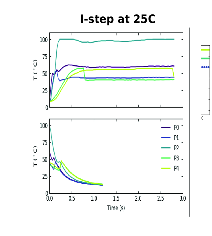
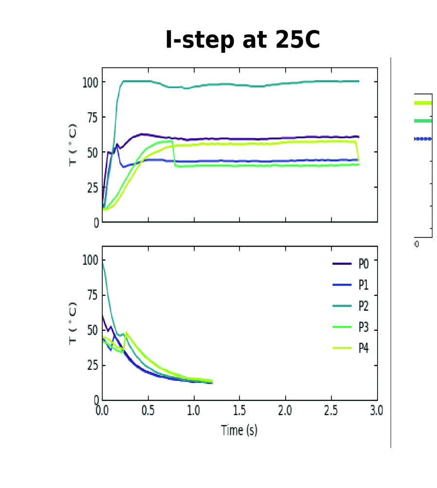
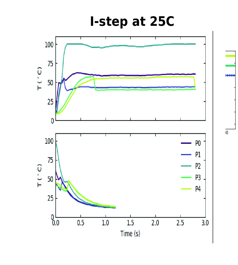
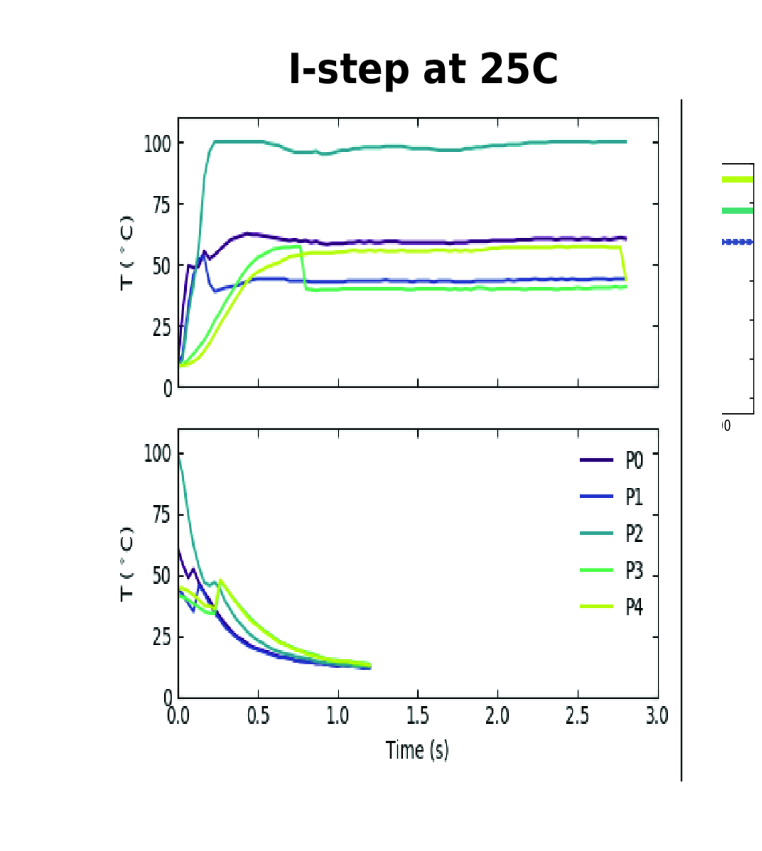
(a)
(b)
(c)
(d)
Figure S6: Current-induced Peltier heating of \ceCa2RuO4.LABEL:sub@fig:Peltier_photo Photograph of the single crystal used for the experiment (Sample #9, CR29G1).
Electrical contact is provided by two gold wires ( in diameter) directly connected to the sample surface and edges by Ag epoxy, without any gold plating.
To minimise the thermal conductivity with the bath at , the sample is resting on cigarette paper without the use of any glue, and the cigarette paper is lifted by about from the underlying sample holder.
LABEL:sub@fig:Peltier_IR Thermal images plotted with the insulating calibration upon driving a positive and negative current through the sample.
The material is kept in the insulating phase for the whole experiment.
LABEL:sub@fig:Peltier_T Thermal temperature close to the left and right electrodes as a function of current.
LABEL:sub@fig:Peltier_dT Difference in temperature between the two electrodes.