Two-dimensional Ga2O3 glass:
a large scale passivation and protection material for monolayer WS2
Atomically thin transition metal dichalcogenide crystals (TMDCs) have extraordinary optical properties that make them attractive for future optoelectronic applications. Integration of TMDCs into practical all-dielectric heterostructures hinges on the ability to passivate and protect them against necessary fabrication steps on large scales. Despite its limited scalability, encapsulation of TMDCs in hexagonal boron nitride (hBN) currently has no viable alternative for achieving high performance of the final device. Here, we show that the novel, ultrathin glass is an ideal centimeter-scale coating material that enhances optical performance of the monolayers and protects them against further material deposition. In particular, capping of commercial grade WS2 monolayers outperforms hBN in both scalability and optical performance at room temperature. These properties make Ga2O3 highly suitable for large scale passivation and protection of monolayer TMDCs in functional heterostructures.
Two-dimensional (2D), atomically thin monolayers of transition metal dichalcogenide crystals (TMDCs) are highly optically active, direct bandgap semiconductors that have emerged as a promising platform for future low-energy electronics, optoelectronics, and photonics [1, 2, 3, 4]. Extensive research points to an exceptional potential of TMDC excitons (stable electron-hole pairs) [5] for ultra-efficient energy and information technologies [6, 7], sensing [8], and fundamental studies of collective quantum phenomena [10, 9]. However, integration of monolayer TMDCs into useful electrical and optical devices by direct material deposition, e.g. of high- dielectric materials for top-gating [11, 12, 13], usually degrades their electronic and optical properties. High optical and electronic performance can be achieved and retained [14, 15] by full encapsulation in mechanically exfoliated hexagonal boron nitride (hBN), commonly used to passivate and protect the monolayers. However, this approach is non-scalable due to the limited size and inconsistent thickness of the exfoliated hBN flakes. Significant effort has been directed towards increasing the size of monolayer TMDCs from several to the -scale [16, 17], and the capability to passivate and protect the monolayers on similar scales is equally important. Without a large scale passivation and protection technology, the realization of multilayer structures with integrated monolayer TMDCs remains challenging and inherently non-scalable.
A practical protection and passivation material should: a) have a uniform, -scale thickness on wafer scale, b) have no negative effects on the optical and electrical properties of monolayer TMDCs, and c) protect against further material deposition to enable the integration into multilayer heterostructures. Here, we introduce an isotropic, 2D glass [18] as a novel material for low-cost passivation and protection of atomically-thin semiconductors. The wide-bandgap 2D Ga2O3 glass can be synthesized under ambient conditions, with a highly reproducible thickness of less than on -scale. By capping the notoriously fragile with 2D Ga2O3, we demonstrate its excellent passivating properties. Our measurements at cryogenic temperatures indicate that the 2D Ga2O3 passivates the commercial grade monolayer by filling in sulphide vacancies. The passivated WS2 exhibits enhanced exciton photoluminscence (PL) and suppressed exciton annihilation processes, similarly to the effects of superacid treatment [19] and full hBN encapsulation [20]. Finally, we show that protects against further deposition of Al2O3, a high- dielectric material. Comparison of the exciton PL of commercial grade monolayer WS2 capped by either Ga2O3 or hBN shows that the 2D glass outperforms hBN as a protective material at room temperature.
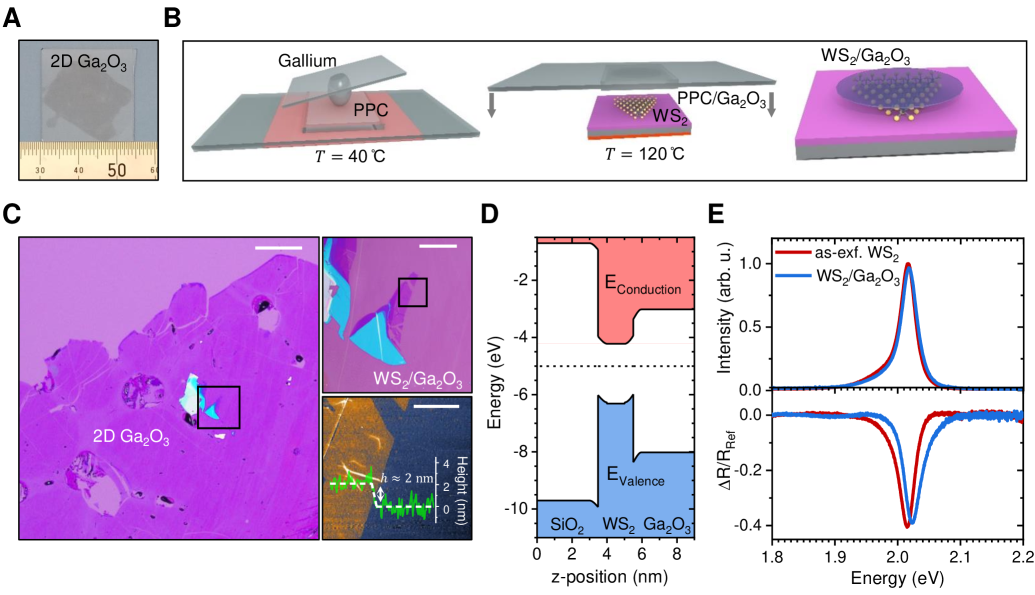
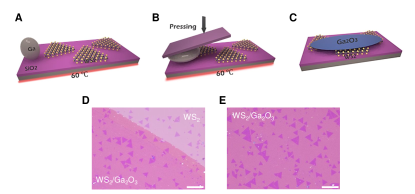
Amorphous Ga2O3 is an electrically insulating, isotropic glass, fully transparent in the visible range [21], and is therefore well suited for protection of optically active materials. The recently discovered liquid metal printing method [18] enables the low-cost synthesis of -sized 2D sheets of Ga2O3 (Fig. 1A) with a reproducible thickness of in ambient conditions [see Supplementary Materials S1]. X-ray photoelectron spectroscopy (XPS) on the 2D Ga2O3 confirms the purity of its stoichiometric composition with 60% oxygen and 40% gallium [see Supplementary Materials S2]. A scanning electron microscope with a transmission diffraction stage was used to measure the crystal structure of synthesized 2D Ga2O3, revealing that it is an entirely amorphous, isotropic glass [see Supplementary Materials S3]. Electron energy loss spectroscopy (EELS) measurements unveiled a bandgap of around [see Supplementary Materials S4], which is significantly wider than the bandgap of amorphous bulk Ga2O3 [21].
We have developed two high-yield techniques for capping monolayer TMDCs with 2D Ga2O3. The first technique is the direct synthesis of Ga2O3 on top of the monolayers, capable of covering large-area TMDCs grown by chemical vapor deposition (CVD) [see Supplementary Materials S5 and S6]. The second technique (Fig. 1B) is the deterministic transfer of 2D Ga2O3, synthesized on spin-coated poly-propylene carbonate (PPC), onto target areas, such as m-sized mechanically exfoliated monolayers [Supplementary Material S7]. These methods were used to create the WS2/Ga2O3 heterostructures with both CVD-grown and exfoliated monolayers. Monolayer WS2 features the largest band gap in the TMDC family [4], and therefore enables us to test whether 2D Ga2O3 glass sufficiently confines the excited charge carriers in the TMDCs. In what follows, we focus on monolayer WS2 mechanically exfoliated from single-crystalline commercial grade bulk crystals, which have superior optical quality compared to the large-scale CVD-grown monolayers used in this work.
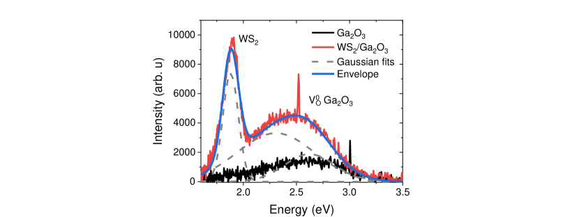
Fig. 1C shows a clean -scale sheet of Ga2O3 deterministically transferred on top of an exfoliated monolayer WS2 [see Supplementary Material S8 for the results on CVD-grown WS2]. The AFM image of the sample surface shows a homogeneous monolayer coverage, with the height profile demonstrating a step size of from the 2D Ga2O3 sheet to the heterostructure. The height difference to the thickness of a bare monolayer WS2 ( [4]) can be attributed to a pronounced van der Waals spacing between the monolayer and the Ga2O3 [22]. The XPS and EELS measurements shown in Supplementary Materials S1 and S4, together with the known material properties of monolayer WS2 [23, 24], amorphous SiO2 [25], and amorphous Ga2O3 [21], allow us to construct a band diagram of the WS2/Ga2O3 heterostructure (see Fig. 1D), while the exact position of the WS2 band edge is still under debate [23, 5, 24]. The identified type I band alignment enables the Ga2O3 to confine the free carriers in the conduction and valence bands of WS2, to form excitons.
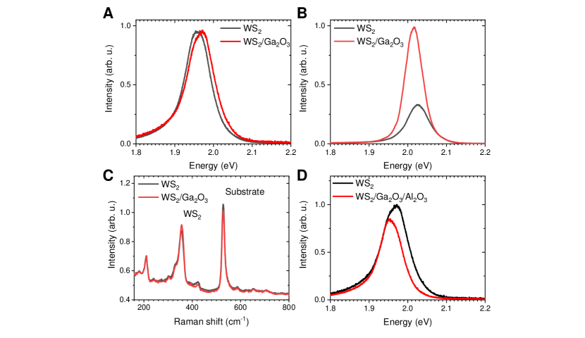
To test the effect of the Ga2O3 capping on the exciton properties of monolayer WS2, we performed PL and reflectivity studies. The system was excited by a ND:YAG continuous wave (cw) laser source with a wavelength of () which is energetically above the band gap of monolayer WS2, but below the band gap of 2D Ga2O3. The reflectivity measurements were performed with a tungsten halogen white light source. The PL and reflectivity spectra of an as-exfoliated monolayer WS2 and of the WS2/Ga2O3 heterostructure under ambient conditions feature the exciton PL and absorption at (Fig. 1E). The excitons in WS2/Ga2O3 have slightly higher energies compared to the as-exfoliated WS2, most likely due to dielectric screening effects in Ga2O3. Nevertheless, the amplitude and the linewidth of the PL and reflectivity spectra are not affected by Ga2O3 capping, indicating that the WS2 excitons are not quenched. The PL and Raman measurements on the CVD-grown monolayers confirm these results, and show that the optical phonon modes of monolayer WS2 remain intact [see Supplementary Materials S8]. By contrast, exciton PL of exfoliated WS2 monolayers passivated with the commercial grade hBN is significantly quenched [see Supplementary Materials S9].
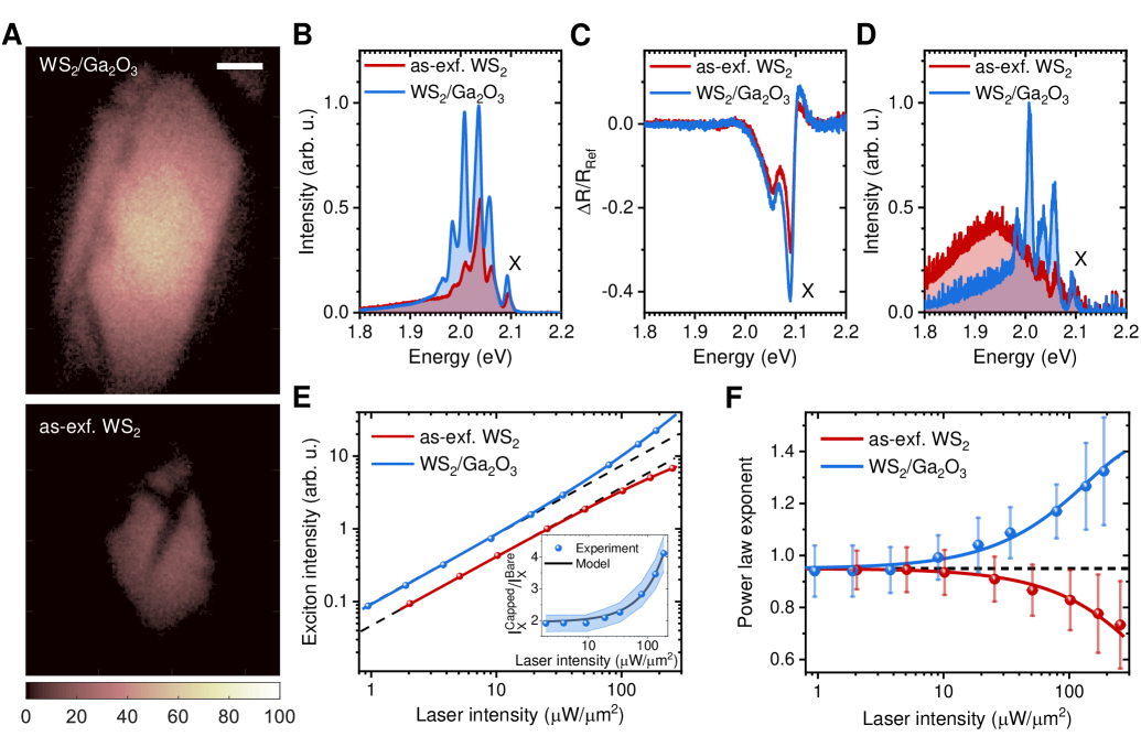
The effect of the Ga2O3 capping on the WS2 exciton PL and absorption was further tested at , when exciton-phonon interactions and thermal effects are suppressed. We excited the as-exfoliated WS2 and the heterostructure with a large Gaussian laser spot of the diameter , which effectively eliminated artefacts due to the sample inhomogeneities by averaging the PL over a large sample area. Fig. 2A contains the corresponding PL intensity maps, showing that both the as-exfoliated WS2 and the heterostructure have a homogeneous PL texture. The PL spectra of the monolayers (Fig. 2B) are composed of multiple distinct PL peaks, including the exciton (), the trion () and additional low energy peaks associated with many-body complexes [4, 26, 27]. The reflectivity spectra (Fig. 2C) of the exfoliated monolayers show strong absorption features at the exciton and trion energies, which indicates that both the uncapped and the capped samples are doped [14]. Since the ratios between the absorption dips for both samples are the same, this effect is not related to the Ga2O3 capping and can be traced to the large density of sulphide vacancies in the commercial grade monolayer WS2 resulting in high intrinsic n-type doping [28].
The PL intensity of the heterostructure is strongly enhanced at cryogenic temperatures (see Fig. 2A,B and Supplementary Materials S8, S10). In particular, at low excitation intensities, the broad bound exciton peak, which dominates the PL spectrum of the as-exfoliated sample around below the free exciton energy [29], is strongly quenched while the PL of the excitons, trions and low-energy states are enhanced (Fig. 2D). This indicates that Ga2O3 capping suppresses formation of bound excitons at sulphide vacancies [30], enhancing the formation of many-body states and the total exciton quantum yield. Indeed, cathodoluminescene (CL) measurements at presented in Supplementary Materials S11, reveal the presence of deep donor-type oxide vacancies in Ga2O3 [31] with a higher concentration of vacancies in the WS2/Ga2O3 heterostructure. This result suggests that the 2D Ga2O3 fills the sulphide vacancies in the WS2 with oxides, which creates donor-type oxide vacancies in the Ga2O3. This mechanism can explain the suppression of bound exciton formation in the WS2/Ga2O3 without affecting its doping level.
To understand the origins of the PL enhancement, we measured the exciton PL of both the as-exfoliated WS2 and the WS2/Ga2O3 heterostructure for a range of laser intensities spanning two orders of magnitude (Fig. 2E). The corresponding PL spectra are shown in Supplementary Materials S10. At laser intensities below W/m2, the exciton intensity of the uncapped monolayers follows the power law, , shown by the dashed lines in Fig. 2E. Without losses, and assuming the direct photon-exciton transition, the dependence is linear: [32]. In our samples, at low laser intensities, , which indicates that the exciton formation experiences intensity-dependent losses, e.g., free-to-bound exciton transitions or formation of many-body exciton complexes (Fig. 2D). However, at laser intensities above W/m2, the exponent of the power law decreases for the as-exfoliated WS2 (see Fig. 2F), in line with previous observations [20]. This behaviour is typically caused by annihilation processes between multiple excitons or between excitons and defects [33], e.g. Auger recombination [34].
In contrast, for the heterostructure the power law exponent remains well above . This indicates that the exciton annihilation in monolayer WS2 is suppressed by Ga2O3 capping, similarly to the effect of full hBN encapsulation [20, 34]. However, the mere suppression of annihilation would result in a linear power law with a constant [20], while in WS2/Ga2O3 the exciton PL transitions from a linear to a nonlinear process with increasing laser intensities (Fig. 3F). This behaviour can be explained with a two-step exciton generation process via the deep oxide vacancies in the 2D Ga2O3 [see Supplementary Materials S12], in addition to the direct electron-hole excitation. The indirect process involves electron tunnelling between the donor-type oxide vacancies and the WS2 valence band as an intermediate step in the WS2 exciton formation. This results in accumulation of exciton densities and growing enhancement of the exciton PL intensity.
By fitting the exciton intensities and the extracted power law exponents of both as-exfoliated WS2 and the heterostructure (see Fig. S2E-F) with the theoretical model [see Supplementary S12], we deduce that the exciton generation rate in the heterostructure is times higher, and that the exciton saturation density dictated by the annihilation processes is times higher compared to the as-exfoliated WS2. These accumulating effects lead to the observed power-dependent enhancement of the exciton PL intensity in WS2/Ga2O3, with an enhancement factor of within our power range (Fig. 2E, inset). Measurements on CVD-grown monolayer WS2 show the same PL intensity enhancement at cryogenic temperatures [Supplementary Materials S8].
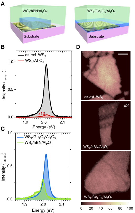
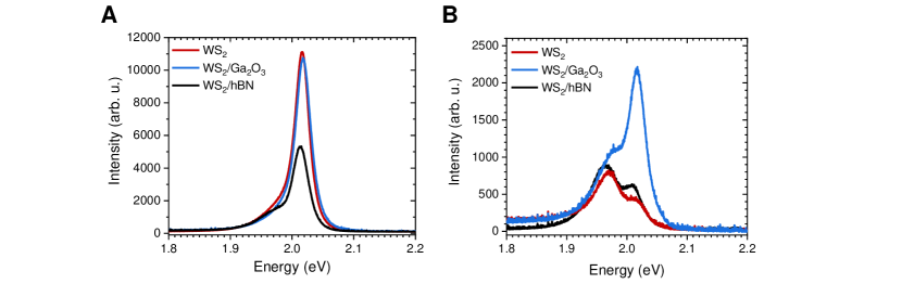
To test the protective capacity of 2D Ga2O3 for device integration, we deposited Al2O3, a high- dielectric material, onto monolayer WS2 capped by either Ga2O3 or exfoliated commercial grade hBN (Fig. 3A). For deposition, we used electron beam evaporation (EBE) with a relatively high electron beam energy to stress-test the protection. As seen in Fig. 3B, direct EBE deposition of Al2O3 on top of bare WS2 strongly quenches the exciton PL [11]. The PL spectra (Fig. 3C) of the hBN and Ga2O3 capped WS2 after EBE of Al2O3 show that both methods protect well against further material deposition, with approximately two orders of magnitude enhancement of exciton PL intensities compared to WS2/Al2O3.
However, the PL spectrum of the hBN-capped WS2 (Fig. 3C) shows a pronounced shoulder at the trion energy () which indicates that it is strongly doped after Al2O3 deposition [see Supplementary Materials S9]. In addition, the hBN flake covers the monolayer only partially, resulting in a relatively small protected area (Fig. 3D). In contrast, the PL spectrum of the WS2/Ga2O3/Al2O3 heterostructure shows strong neutral exciton PL with around of the exciton intensity of an as-exfoliated WS2 monolayer. The PL texture of the WS2/Ga2O3/Al2O3 is homogeneous (Fig. 3D), which highlights the homogeneity of the coverage.
The PL measurements on Ga2O3-capped CVD-grown monolayer WS2 support these observations [see Supplementary Materials S8].
To summarise, the novel 2D Ga2O3 glass shows great potential as a low-cost and practical wide-bandgap, isotropic material for scalable passivation of monolayer WS2. Capping the monolayers with Ga2O3, either by direct printing or by deterministic transfer, fully preserves their exciton properties in ambient conditions. At cryogenic temperatures, the Ga2O3 passivation significantly enhances the optical performance of WS2 by suppressing bound exciton formation at the sulphide vacancies, promoting nonlinear exciton generation, and suppressing the exciton annihilation processes. These findings provide a pathway towards high-performance surface-passivated TMDC/Ga2O3 heterostructures on a -scale, e.g., by combining the large-scale mechanical exfoliation [17] with the Ga2O3 capping. Finally, our finding that 2D Ga2O3 glass outperforms hBN for protecting commercial grade monolayer WS2 against high- dielectric material deposition breaks new ground for the integration of monolayer TMDCs into large-area 2D devices.
References
- [1] K. F. Mak, J. Shan, Nature Photonics 10, 216-226 (2016).
- [2] Q. H. Wang, K. Kalantar-Zadeh, A. Kis, J. N. Coleman, M. S. Strano, Nature Nanotechnology 7, 699-712 (2012).
- [3] A. K. Geim, I. V. Grigorieva, Nature 499, 419-425 (2013).
- [4] T. Mueller, E. Malic, npj 2D Materials and Applications 2, 29 (2018).
- [5] A. Chernikov et al., Physical Review Letters 113, 076802 (2014).
- [6] K. F. Mak, K. L. McGill, J. Park, P. L. McEuen, Science 344, 1489-1492 (2014).
- [7] B. Radisavljevic et al., Nature Nanotechnology 6, 147-150 (2011).
- [8] S. Manzeli et al., Nature Communications 10, 4831 (2019).
- [9] Z. Wang et al., Nature 574, 76-80 (2019).
- [10] M. M. Fogler, L. V. Butov, K. S. Novoselov, Nature Communications 5, 4555 (2014).
- [11] S. Y. Kim, H. I. Yang, W. Choi, Applied Physics Letters 113, 133104 (2018).
- [12] K. M. Price et al., ACS Applied Nano Materials 2, 4085-4094 (2019).
- [13] J.-G. Song et al., ACS Applied Materials and Interfaces 8, 28130-28135 (2016).
- [14] M. Sidler et al., Nature Physics 13, 255-261 (2017).
- [15] J. Gu et al., Nature nanotechnology 14, 1024-1028 (2019).
- [16] J. Lee et al., Advanced Materials 29, 1702206 (2017).
- [17] F. Liu et al., Science 367, 903-906 (2020).
- [18] A. Zavabeti et al., Science 358, 332-335 (2017).
- [19] M. Amani et al., Science 350, 1065-1068 (2015).
- [20] Y. Hoshi et al., Physical Review B 95, 241403(R) (2017).
- [21] J. Kim et al., NPG Asia Materials 9, e359 (2017).
- [22] R. S. Datta et al., Nature Electronics 3, 51-58 (2020).
- [23] H. L. Zhuang, R. G. Hennig, J. Phys. Chem. C 117, 40, 20440-20445 (2013).
- [24] H. Terrones, F. López-Urías, M. Terrones, Scientific Reports 3, 1549 (2013).
- [25] V. Astašauskas et al., Journal of Electron Spectroscopy and Related Phenomena 241 146829 (2020).
- [26] P. Nagler et al., Physical Review Letters 121, 057402 (2018).
- [27] S.-Y. Chen et al., Nature Communications, 9, 3717 (2018).
- [28] S.-S. Chee et al., Nanoscale 9, 9333 (2017).
- [29] C. Cong et al., Advanced Optical Materials 6, 1700767 (2018).
- [30] V. Carozo et al., Science Advances 3, e1602813 (2017).
- [31] J. B. Varley et al., Applied Physics Letters 97, 142106 (2010).
- [32] C. Spindler et al., Journal of Applied Physics 126, 175703 (2019).
- [33] G. Moody, J. Schaibley, X. Xu, Journal of the Optical Society of America B 33, C39-C49 (2016).
- [34] J. Zipfel et al., Physical Review B 101, 115430 (2020).
Supplementary Materials
Material properties of 2D Ga2O3.
S1: Atomic force microscopy of 2D Ga2O3 and WS2/Ga2O3 heterostructures.
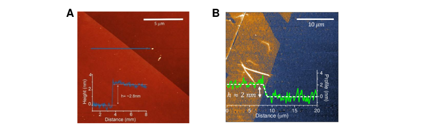
The surface morphology and thicknesses of the 2D Ga2O3 sheet and of WS2/Ga2O3 were explored by atomic force microscopy (AFM). The AFM measurements were collected using a Bruker Dimension Icon AFM with Scanasyst-air AFM tips. Gwyddion 2.36 software was employed for the AFM image processing and analysis. As seen in (Fig. S1A), the typical step height from the substrate to the Ga2O3 is . The step height from the Ga2O3 sheet to the heterostructure is (Fig. S1B).
S2: X-ray photoelectron spectroscopy of 2D Ga2O3.
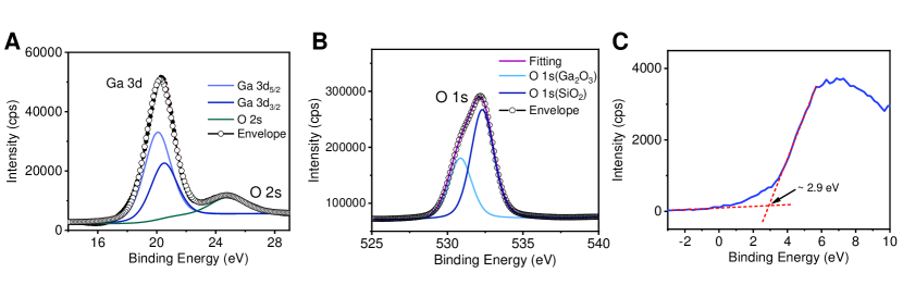
X-ray photoelectron spectroscopy (XPS) was carried out to explore the chemical bonding states of 2D Ga2O3. Fig. S2A-B illustrate the spectra of Ga 3d and O 1s regions, respectively, for the Ga2O3. The characteristic broad peak of the Ga 3d region centred at , is deconvoluted into and components attributed to the presence of the Ga3+ state in Ga2O3 [35]. No peak is detected in the Ga 3d region associated with elemental gallium (Ga0). The peak located at in the Ga 3d region corresponds to the broad O 2s feature [36]. The peak deconvolution of the O 1s presented in Fig. S2B signals the presence of two oxygen species with binding energies of and . The peak with the higher binding energy is related to the Si-O-Si bond and the peak at is the contribution from the Ga2O3 [35].
The valence band XPS spectrum presented in Fig. S2C reveals that the energy difference between the valence band maximum and the Fermi energy is . The XPS spectrum was measured using a Thermo Scientific Kα XPS spectrometer equipped with a monochromatic Al Kα source () with a spot size of approximately . All the core-level spectra (Ga 3d, O 1s, C 1s, etc.) were recorded with a pass energy of . XPS data acquisition and peak fitting analysis was done using the dedicated XPS Avantage software.
S3: Crystallinity of 2D Ga2O3.
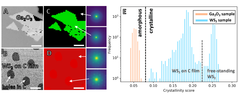
To assess the crystal structure of both the synthesized 2D Ga2O3 and monolayer WS2 used in this article, we used a modified Zeiss Gemini 500 scanning electron microscope (SEM) with a transmission diffraction stage [37] and acquired a map of 80 by 80 electron diffraction patterns for 2D Ga2 and 50 by 50 electron diffraction patterns for monolayer WS2. The microscope operated at for 2D Ga2O3 and at for monolayer WS2 with a beam size of roughly and a step size in between patterns of around for 2D Ga2O3 and for monolayer WS2. Each pattern was recorded with an exposure time of .
Fig. S3A-B shows virtual images of 2D Ga2O3 and of a WS2 monolayer. To determine whether the material is crystalline or amorphous, the diffraction patterns were analyzed for clusters of intensity (diffraction spots) with a self-made script that utilizes the Python package trackpy [38]. A histogram of the algorithm output for the two samples (Fig. S3E) shows a sharp threshold between the amorphous and crystalline phases, beyond which patterns with spots would be situated. Applying the threshold and converting the data back results in the maps in Fig. S3C-D, which show two examples for the scattering observed from the amorphous 2D Ga2O3 and from the single-crystalline WS2. This analysis demonstrates that 2D Ga2O3 sheets used in our experiments are amorphous.
S4: Optical band gap of 2D Ga2O3.
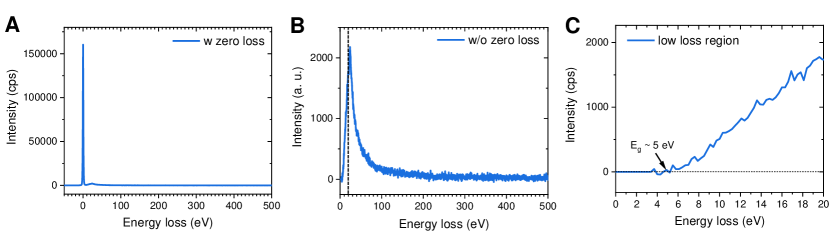
To determine the bandgap of a synthesized 2D Ga2O3 sheet via electron energy loss spectroscopy (EELS), the Ga2O3 was transferred onto a transmission electron microscope (TEM) grid. For this measurement, the TEM model JEOL JEM-2100f operating at the acceleration voltage of and equipped with the Gatan Tridium imaging filter was used. EELS measures the change in the kinetic energy of electrons after interactions with the sample, and the EELS spectrum at lower binding energies () can reveal the bandgap of materials. In the low-loss region the intensity of electrons that pass through the sample without experiencing any losses dominate the spectrum (Fig. S4A). This zero-loss peak needs to be removed before the inelastic interactions between the sample and the electron beam can be analysed. Here, the zero-loss peak is centred at with a full-width-at-half-maximum (FWHM) of less than , thus featuring a reliable technique for measuring materials with a wide bandgap, including Ga2O3. The EELS measurement was conducted in the scanning transmission electron microscope (STEM) mode. The software Digital Micrograph v1.84 was used to analyse and remove the zero-peak loss. The resulting EELS spectrum is presented in Fig. S4B for the energy range up to . The optical bandgap of the Ga2O3 sheet corresponds to the onset of the EELS-spectrum in the low-loss region (here, ) and, according to Fig. S4C, is located at .
Fabrication of WS2/Ga2O3 heterostructures.
S5: Fabrication and transfer of CVD-grown monolayer WS2.
Monolayer WS2 crystals are grown on a sapphire [Al2O3 (0001)] substrate by a chemical vapor deposition (CVD) process, similar to the method reported in [39]. Therefore, the WO3 and S powders are placed in separate quartz crucibles and located at the upstream region of a tubular quartz reactor, followed by the sapphire substrate in the downstream region. Further, the WO3 and S powders are heated up to and , with the temperature rates of and , respectively. The growth of the WS2 is finished after reaching these temperatures.
After the growth, monolayer WS2 crystals can be transferred by means of the polymer-assisted wet transfer technique [39]. In this work, polystyrene (Mw=192 000) (PS) in toluene solution (50 mg ml-1) is used for the transfer onto a Si/SiO2 substrate. First, PS is spin-coated on top of the CVD-grown monolayers at 3000 rpm for 60 s and then baked at for . After the baking process, a 2 mol L-1 NaOH solution is used to delaminate the PS/WS2 crystal film from the sapphire substrate. To remove the remaining alkali residues, the film is placed in a deionized water bath. Finally, the PS film is picked up from the bath with the Si/SiO2 target substrate and dissolved in acetone, which leaves the monolayers transferred on the substrate surface. As a result, we fabricated and transferred a large area of monolayer WS2 crystals on top of a Si/SiO2 substrate.
S6: Direct synthesis method.
To synthesize 2D Ga2O3 directly on top of monolayer TMDCs, we utilized the liquid gallium printing technique for making ultrathin sheets of Ga2O3[18, 40]. Gallium has a melting point of [41] and is therefore liquid at temperatures which are harmless for monolayer TMDCs. In air, the surface of liquid gallium transforms to a ultrathin Ga2O3 shell due to the self-limiting oxidation process [18], which is more effective at elevated temperatures.
In this work, the samples were fabricated on a hot plate at in air to accelerate the oxidization process without damaging the monolayers. To start the synthesis, a small liquid gallium droplet is placed on the sample surface next to the monolayer WS2 area (Fig. S6A). Further, the ultrathin Ga2O3 shell of the droplet is brought in contact with the monolayer area by squeezing the droplet with another piece of a Si/SiO2 wafer on top of the sample with the aid of tweezers (Fig. S6B). Careful separation of the small substrate from the sample is crucial for the Ga2O3 sheet to fully delaminate from the gallium and to be transferred on top of monolayer WS2 (Fig. S6C). After the transfer, a triangle-shaped CVD-grown monolayer WS2 covered with 2D Ga2O3 can be easily found on a large area of the sample surface. The excess gallium residues can be removed by gently washing the sample in an ethanol or a methanol bath. As result of this process, we achieved direct synthesis of 2D Ga2O3 on top of a large scale area of CVD-grown monolayer WS2 ( Fig. S6D-E).
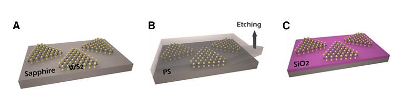
S7: Deterministic transfer method.
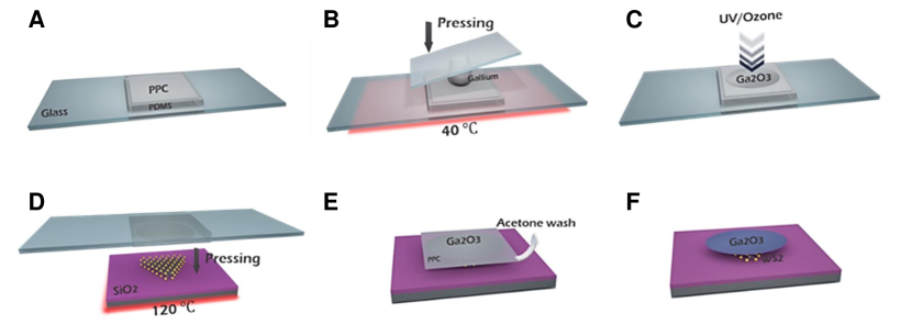
Unlike the direct deposition method discussed above (see section S6), the deterministic transfer of liquid metal synthesized 2D Ga2O3 requires an additional sacrificial polymer layer. Therefore, we used poly-propylene carbonate (PPC) with a low thermal stability and a glass transition at around [42]. First, the PPC in anhydrous anisole solution is spin-coated at for on top of an elastomer stamp (poly dimethyl siloxane, PDMS) and further baked at for . A glass slide is used to stabilize the PDMS stamp during this process (Fig. S7A). Next, 2D Ga2O3 is directly synthesized on top of the PPC layer as described in section S6, but with a synthesis temperature of to prevent damage of the temperature sensitive PPC layer (Fig. S7B). Using an optical microscop, a clean, gallium-free area can be marked and selected for capping the TMDC monolayer. A UV/ozone treatment is subsequentially applied on the Ga2O3 surface for to remove the organic residues and to fully oxidize it (Fig. S7C).
Monolayer WS2 is prepared by exfoliation from a commercial grade bulk WS2 crystal (sourced from HQ Graphene) using the conventional scotch tape technique [43], and then transferred on top of a Si/SiO2 substrate. Our exfoliated monolayers are limited to the scale due to the limitations of the scotch tape method. Next, the monolayer is aligned with the targeted Ga2O3 area by using a transfer stage with integrated heating (Fig. S7D). Before bringing the sample surface in contact with the 2D Ga2O3, the sample is heated up to , i.e. above the glass phase transition of the PPC. This temperature allows the PPC to follow the sample surface morphology upon contact. After contact, the sample is further heated up to to release the PPC [40], with a temperature rate of to avoid any strain between the substrate, the monolayer, and the Ga2O3. This temperature is held for to fully soften the PPC. After that, the PPC layer easily separates from the stamp by slowly lifting it up with the transfer stage and by doing so the transfer of 2D Ga2O3 is achieved (Fig. S7E). Subsequently, the sample is placed in a cold acetone bath to dissolve the PPC residues, followed by an isopropyl and an ethanol bath to remove any organic residues left (Fig. S7F). Fig. 1E shows that this cleaning procedure does not affect the optical properties of the WS2/Ga2O3 heterostructure.
Photoluminenscence studies on the heterostructures.
S8: Spectroscopy on CVD-grown WS2 capped by Ga2O3:
To test the direct synthesis approach (see section S6), we performed the photoluminescence (PL ) and Raman spectroscopy on CVD-grown monolayer WS2 passivated and protected by 2D Ga2O3. Fig. S8A and S8B show the PL spectra at and at respectively. In agreement with the results from the main text, the Ga2O3 capping does not quench the monolayer PL at room temperature and causes significant PL intensity enhancement at cryogenic temperatures. Hence, these properties are independent on the transfer technique. The Raman spectra at (Fig. S8C) show that the capping does not affect the optical phonons in the heterostructure, and therefore indicate that the 2D Ga2O3 does not affect the crystal structure of monolayer WS2.
The PL spectra after EBE deposition of Al2O3 (Fig. S8D) further confirm that 2D Ga2O3 capping protects monolayer WS2 against dielectric material deposition, which is the first step towards integrating the CVD-grown monolayers into complex multilayer heterostructures on large scales. For this experiment, we used a relatively low electron-beam energy for the EBE deposition.
S9: Comparison between Ga2O3 and hBN capping of monolayer WS2.
In order to compare the passivating and protecting properties of 2D Ga2O3 and hBN, we prepared a WS2/hBN heterostructure with a thin exfoliated hBN flake. Remarkably, the PL spectrum of the hBN-capped monolayer shows significant quenching of the exciton PL under ambient coniditions, while the Ga2O3 capping fully conserves the monolayer PL (Fig. S9A). As explained in the main text, sulphide vacancies in monolayer WS2 can have a large impact on the doping level, the exciton formation, and consequently on the exciton, trion and bound exciton PL [44, 30, RN553]. In air, these vacancies can be passivated with O2 [45] or dipolar H2O molecules, and their effect on the PL is reduced. In vacuum, on the other hand, the sulphide vacancy-induced doping strongly affects the PL spectra of monolayer WS2, in which the trion () has a pronounced PL feature compared to the exciton (Fig. S9B). With the hBN capping, the passivating molecules can be squeezed out of the WS2/hBN interface and the sulphide vacancy-induced doping effect becomes more significant (Fig. S9A). In vacuum, the remaining passivating molecules are removed from the interface, which leads to strong sulphide vacancy-induced doping effect (Fig. S9B). On the contrary, with Ga2O3 capping, the sulphide vacancies can be passivated with oxides from the 2D Ga2O3 as explained in the main text, and the emerging donor-type oxide vacancies in the Ga2O3 can be passivated with O2 or the bipolar H2O molecules from air. This passivation of the sulphide vacancies leads to strongly reduced doping effect in vacuum (Fig. S9B).
These results demonstrate that 2D Ga2O3 outperforms exfoliated hBN flakes for passivation of commercial grade monolayer WS2 in terms of both scalability and optical performance.
WS2/Ga2O3 at cryogenic temperatures.
S10: Intensity-dependent PL of WS2 and WS2/Ga2O3 at cryogenic temperature.
We performed intensity-dependent PL measurements to investigate the impact of the Ga2O3 capping on the WS2 excitons at cryogenic temperatures (). Fig. S10A-C show the PL spectra of both capped and of uncapped monolayer WS2 at three values of laser intensities () spanning more than two orders of magnitude. At the uncapped monolayer WS2 shows strong PL from the bound excitons at [29], while the capped monolayer shows strongly enhanced PL from the the many-body exciton complexes at the energies below . The suppression of the bound exciton formation can be attributed to passivation of the sulphide vacancies with oxides from Ga2O3 (see main text). At , the strong enhancement of the many-body complexes is clearly visible in the PL spectrum ( Fig. S10B), while the PL peak from the biexciton () experiences a nonlinear increase in intensity compared to the other peaks. Following this nonlinear increase, the biexciton PL dominates the spectrum at high laser intensities (Fig. S10C), which is in agreement with previous reports [26].
Most importantly, the exciton PL intensities (insets Fig. S10A-C) clearly show the laser intensity dependent enhancement in the capped sample, which can be associated with suppression of bound exciton formation, suppressed Auger recombination, and increasing electron-hole injection from the Ga2O3 sheet (see section S12 for details).
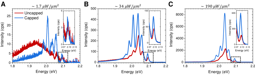
S11: Low temperature cathodoluminescence of WS2/Ga2O3 heterostructure
By using an SEM equipped with a spectrometer, we carried out cathodoluminescence (CL) measurements at to investigate the defect energies in the WS2/Ga2O3 heterostructure. Fig. S11 shows the CL spectra of both the 2D Ga2O3 sheet and the heterostructure. The spectra were recorded after exciting the samples with an electron beam with the energy of . The high energy electron beam can excite electrons from the valence band into the vacuum regime or into the conduction band, dependent on the inelastic scattering between the electron beam and the structure. After excitation, the electrons from the conduction band or the electrons from donor type vacancies can recombine with the excited holes in the valence band. If the transitions are optically allowed, this recombination process creates photons with energies corresponding to the energy differences between the electrons and the holes, and a spectrometer can be used to measure the photon energies. The CL spectrum of the WS2/Ga2O3 has two peaks with and while the CL spectrum of the Ga2O3 has a weaker pronounced feature at (Fig. S11). The spectrum of the heterostructure can be well reproduced with three Gaussian peaks with the central energies of , and . According to previous reports [46, 47, 48], the peak corresponds to the CL spectrum of monolayer WS2 and the higher energy peaks correspond to oxide vacancies in the Ga2O3. While, according to the Gaussian fits, the CL spectra of the Ga2O3 sheet and the WS2/Ga2O3 heterostructure have a similar intensity at around , the emission from the vacancies is strongly enhanced in the heterostructure (Fig. S11). This is an evidence of a significantly higher density of the new donor-type oxide vacancies in the heterostructure compared to the bare Ga2O3 sheet.
Together with the suppression of bound exciton formation (see Fig. S10A in section S10), these results suggests that the oxides from the Ga2O3 sheet fill the sulphide vacancies in WS2, which leads to the increase of the donor-type oxide vacancy density in the heterostructure, while the doping level is not affected (see Fig. 2B in the main text).
S12: Theoretical model for the exciton generation in the WS2/Ga2O3 heterostructure.
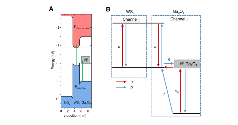
To model the intensity dependent exciton PL intensities for both the capped and uncapped monolayer WS2, we constructed a rate equation model, which accounts for the direct exciton-hole generation in monolayer WS2, as well as for the indirect electron-hole generation via the oxide vacancies in the Ga2O3 sheet. Fig. S12.1A shows the band diagram of the SiO2/Ga2O3 heterostructure including the optically active oxide vacancies with the energies extracted from the CL measurement (Fig. S11). According to this band diagram, the energies of the donor type oxide vacancies are above the WS2 valence band maximum. Hence, the donor electrons can tunnel into the excited WS2 holes which is crucial for the process described here.
After tunnelling, a laser source with sufficient energy can replenish the empty oxide vacancies by exciting the Ga2O3 valence band electrons, and further excite the tunnelled electrons from the Ga2O3 into the WS2 conduction band. Finally, the excited electrons can couple to the tunnelled and thermalized holes from the Ga2O3 valence band forming excitons. The efficiency of this two-step process scales with the number of excited WS2 holes. Therefore, with growing intensity, , this effect leads to an increasing power law exponent for the exciton intensity . In other words, the excited WS2 holes effectively catalyse the electron-hole generation in Ga2O3 which competes against the direct exciton formation. Hence, this process delays the exciton formation, and ultimately the electron-hole recombination, leading to a significant increase of the exciton density at high excitation intensities. Moreover, since the Ga2O3 is highly transparent to the laser used in our experiment with , this process has a negligible effect on the direct exciton generation in monolayer WS2.
Fig. S12.1B schematically shows the band diagram of the WS2/Ga2O3 heterostructure with the highlighted transitions for the direct electron-hole pair generation in the monolayer WS2 (Channel I) and for the indirect electron-hole generation via the oxide vacancies (Channel II). For the rate equations, we only consider the formation of exctions, and disregard the formation of trions and other many-body complexes. Therefore, we only take into account the contribution of the donor electrons to the exciton formation and not to the formation of charged particles, e.g. trions.
The process depicted in Fig. S12.1B can be described by the following rate equations:
| (1) | ||||
| (2) | ||||
| (3) | ||||
| (4) |
with the excitation intensities , the electron-hole excitation rate in the monolayer WS2, the density of excited electrons and holes in the monolayer WS2, the donor electron excitation rate , the density of excited donor electrons ( total donor density), the number of excited holes in the Ga2O3 sheet, the donor electron tunnelling rate into the excited WS2 holes, the tunnelling and thermalization rate for into the monolayer WS2, and the exciton formation rate .
In order to account for exciton annihilation processes (e.g., Auger recombination) in this model, we recalculate the exciton density by using an effective loss factor:
| (5) |
where . Here phenomenologically describes the exciton density dependent two-particle annihilation processes [20] between multiple excitons [33, 49, 50], between excitons and defects [33, 49, 51], and between free carriers and defects [33], assuming an equilibrium between generated and annihilated excitons at high exciton densities above the saturation density what leads to :
| (6) |
The factor accounts only for two particle annihilation, but not for other excitation intensity dependent processes, e.g. exciton Mott transition [52], biexciton formation [26] and heating effects, which would lead to additional effective quantum yield losses at high excitation intensities. To verify this phenomenological model, we fitted to the experimental intensity dependent PL measurements, and achieved a good fit to both the exciton intensities and to the extracted power law exponent with for the uncapped sample (see Fig. 2C). Hence, the phenomenological loss factor adequately describes the effective annihilation processes we observe in the uncapped WS2 monolayer within our experimental intensity range. In the experiment, corresponds to in our spectrometer camera.
Assuming that all the generated excitons contribute to the exciton PL, we simulated the excitation intensity dependent exciton PL for the rate equations including the function (eq. (6)), without () and with () the active Channel II in Fig. S12.2B.
The results for excitation intensities spanning six orders of magnitudes are presented in Fig. S12.2A-F. For the simulations, we used the fitted parameters for the exciton PL intensities of the WS2/Ga2O3 heterostructure from Fig. 2C, but for simplicity treated them as dimensionless: , , , , and . Here, the zero-offset of is described by , and the line shape of by the ratio . The value of this ratio is in agreement with the high optical transmissivity of the Ga2O3 sheet compared to monolayer WS2, and we achieved a good fit to the experimental data with this value. The other free parameters dictate whether the vacancies are exhausted at high excitation intensities for the indirect exciton generation process (). This is unlikely within our experimental excitation intensity range, since the trion to exciton ratio is still significant at high intensities in the WS2/Ga2O3 heterostructure (Fig. S10C), which justifies the selected values for , and . For comparison, we calculated the exciton intensities for , and . Fig. S12.2A and S12.2D show the corresponding excitation intensity dependent functions with deactivated and activated Channel II respectively, showing that asymptotically approaches 1 at high excitation intensities for a finite , as observed phenomenologically.
First, we discuss the simulation results without the exciton annihilation processes (). With the deactivated Channel II, the exciton intensity strictly follows a power law with (see Fig.S12.2B-C), confirming that Channel I of our model describes the direct photon-exciton transition leading to the exciton generation in monolayer WS2. With Channel II active, the power law exponent transitions from to with increasing excitation intensity (see Fig. S12.2E-F), which is in agreement with our experimental results (see Fig. 2C).
With finite and without Channel II active, one can clearly see the deviation from the strict power law at high excitation intensities (Fig. S12.2C and S12.2E) which is in agreement with previous reports on exciton annihilation processes in monolayer TMDCs [20] and with our measurements. With smaller , the power law is more affected, as expected.
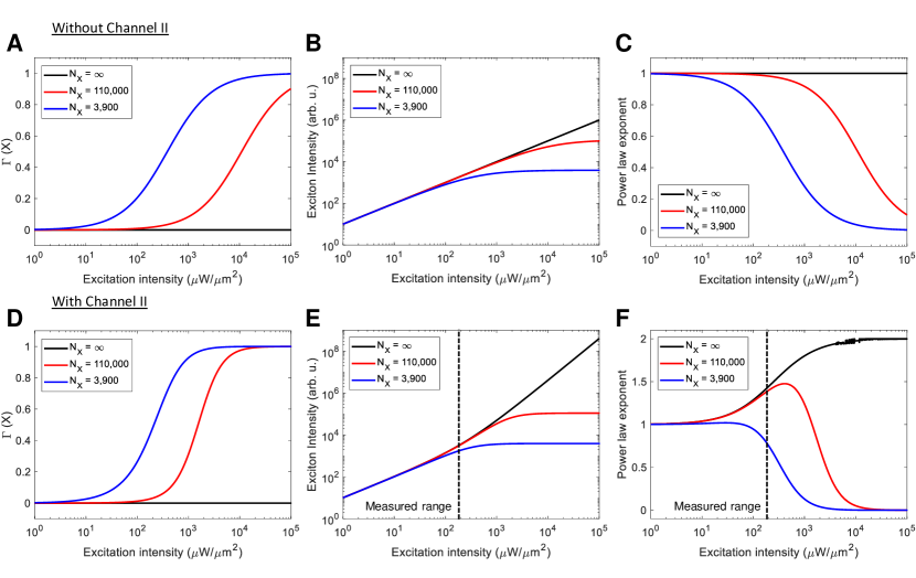
With Channel II active, the exciton annihilation processes strongly limits the nonlinear growth of the exciton intensity and the maximum exciton density is reached at lower excitation intensities, , compared to the case with deactivated Channel II. With , which is the fitted maximum exciton density for the uncapped monolayer (Fig. 2C in the main text), the power law exponent drops below 1 at excitation intensities above (see Fig. 12.2F), showing that the maximum exciton density of the capped sample has to be higher than that of the uncapped monolayer. With an increased saturation density of , the power law exponent peaks around and drops strongly at , at intensities more than one order of magnitude above the experimental intensity range (marked area in Fig. S12.2E-F). This means that due to the Ga2O3-induced nonlinear exciton generation in monolayer WS2, the maximum exciton density is reached at lower excitation intensities compared to the uncapped monolayer. The competition of the hole recycling process with the exciton formation processes allows for significantly higher exciton densities at lower excitation intensities.
By using the model with both Channel I and Channel II, and by modifying the exciton density with the phenomenological loss factor , we achieved a good fit for the measured exciton intensities (Fig. 2C in the main text), with for the uncapped monolayer and with for the capped monolayer. This indicates that the saturation density in the WS2/Ga2O3 heterostructure is enhanced by times compared to the uncapped sample.
References
- [1] K. F. Mak, J. Shan, Photonics and optoelectronics of 2D semiconductor transition metal dichalcogenides, Nature Photonics 10, 216226 (2016).
- [2] Q. H. Wang, K. Kalantar-Zadeh, A. Kis, J. N. Coleman, M. S. Strano, Electronics and optoelectronics of two-dimensional transition metal dichalcogenides, Nature Nanotechnology 7, 699-712 (2012).
- [3] A. K. Geim, I. V. Grigorieva, Van der Waals heterostructures, Nature 499, 419-425 (2013).
- [4] T. Mueller, E. Malic, Exciton physics and device application of two-dimensional transition metal dichalcogenide semiconductors, npj 2D Materials and Applications 2, 29 (2018).
- [5] A. Chernikov, T. C. Berkelbach, H. M. Hill, A. Rigosi, Y. Li, O. B. Aslan, D. R. Reichman, M. S. Hybertsen, T. F. Heinz, Exciton Binding Energy and Nonhydrogenic Rydberg Series in Monolayer WS2, Physical Review Letters 113, 076802 (2014).
- [6] K. F. Mak, K. L. McGill, J. Park, P. L. McEuen, The valley Hall effect in MoS2 transistors, Science 344, 1489-1492 (2014).
- [7] B. Radisavljevic, A. Radenovic, J. Brivio, V. Giacometti, A. Kis, Single-layer MoS2 transistors, Nature Nanotechnology 6, 147-150 (2011).
- [8] S. Manzeli, D. Dumcenco, G. Migliato Marega, A. Kis, Self-sensing, tunable monolayer MoS2 nanoelectromechanical resonators, Nature Communications 10, 4831 (2019).
- [9] Z. Wang, D. A. Rhodes, K. Watanabe, T. Taniguchi, J. C. Hone, J. Shan, K. F. Mak, Evidence of High-Temperature Exciton Condensation in Two-Dimensional Atomic Double Layers, Nature 574, 76-80 (2019).
- [10] M. M. Fogler, L. V. Butov, K. S. Novoselov, High-temperature superfluidity with indirect excitons in van der Waals heterostructures, Nature Communications 5, 4555 (2014).
- [11] S. Y. Kim, H. I. Yang, W. Choi, Photoluminescence quenching in monolayer transition metal dichalcogenides by Al2O3 encapsulation, Applied Physics Letters 113, 133104 (2018).
- [12] K. M. Price, S. Najmaei, C. E. Ekuma, R. A. Burke, M. Dubey, A. D. Franklin, Plasma-Enhanced Atomic Layer Deposition of HfO2 on Monolayer, Bilayer, and Trilayer MoS2 for the Integration of High- Dielectrics in Two-Dimensional Devices, ACS Applied Nano Materials 2, 4085-4094 (2019).
- [13] J.-G. Song, S. J. Kim, W. J. Woo, Y. Kim, I.-K. Oh, G. H. Ryu, Z. Lee, J. H. Lim, J. Park, H. Kim, Effect of Al2O3 Deposition on Performance of Top-Gated Monolayer MoS2-Based Field Effect Transistor, ACS Applied Materials and Interfaces 8, 28130-28135 (2016).
- [14] M. Sidler, P. Back, O. Cotlet, A. Srivastava, T. Fink, M. Kroner, E. Demler, A. Imamoglu, Fermi polaron-polaritons in charge-tunable atomically thin semiconductors, Nature Physics 13, 255-261 (2017).
- [15] J. Gu, B. Chakraborty, M. Khatoniar, V. M. Menon, A room-temperature polariton light-emitting diode based on monolayer WS2, Nature Nanotechnology 14, 1024-1028 (2019).
- [16] J. Lee, S. Pak, P. Giraud, Y.-W. Lee, Y. Cho, J. Hong, A-R. Jang, H.-S. Chung, W.-K. Hong, H. Y. Jeong, H. S. Shin, L. G. Occhipinti, S. M. Morris, S. N. Cha, J. I. Sohn, J. M. Kim, Thermodynamically Stable Synthesis of Large-Scale and Highly Crystalline Transition Metal Dichalcogenide Monolayers and their Unipolar n-n Heterojunction Devices, Advanced Materials 29, 1702206 (2017).
- [17] F. Liu, W. Wu, Y. Bai, S. H. Chae, Q. Li, J. Wang, J. Hone, X.-Y. Zhu, Disassembling 2D van der Waals crystals into macroscopic monolayers and reassembling into artificial lattices, Science 367, 903-906 (2020).
- [18] A. Zavabeti, J. Z. Ou, B. J. Carey, N. Syed, R. Orell-Trigg, E. L. H. Mayes, C. Xu, O. Kavehei, A. P. O’Mullane, R. B. Kaner, K. Kalantar-zadeh, T. Daeneke, A liquid metal reaction environment for the room-temperature synthesis of atomically thin metal oxides, Science 358, 332-335 (2017).
- [19] M. Amani, D.-H. Lien, D. Kiriya, J. Xiao, A. Azcatl, J. Noh, S. R. Madhvapathy, R. Addou, S. KC, M. Dubey, K. Cho, R. M. Wallace, S.-C. Lee, J.-H. He, J. W. Ager III, X. Zhang, E. Yablonovitch, A. Javey, Near-unity photoluminescence quantum yield in MoS2, Science 350, 1065-1068 (2015).
- [20] Y. Hoshi, T. Kuroda, M. Okada, R. Moriya, S. Masubuchi, K. Watanabe, T. Taniguchi, R. Kitaura, T. Machida, Suppression of exciton-exciton annihilation in tungsten disulfide monolayers encapsulated by hexagonal boron nitrides, Physical Review B 95, 241403(R) (2017).
- [21] J. Kim, T. Sekiya, N. Miyokawa, N. Watanabe, K. Kimoto, K. Ide, Y. Toda, S. Ueda, N. Ohashi, H. Hiramatsu, H. Hosono, T. Kamiya , Conversion of an ultra-wide bandgap amorphous oxide insulator to a semiconductor, NPG Asia Materials 9, e359 (2017).
- [22] R. S. Datta, N. Syed, A. Zavabeti, A. Jannat, M. Mohiuddin, M. Rokunuzzaman, B. Y. Zhang, M. Ataur Rahman, P. Atkin, K. A. Messalea, M. B. Ghasemian, E. Della Gaspera, S. Bhattacharyya, M. S. Fuhrer, S. P. Russo, C. F. McConville, D. Esrafilzadeh, K. Kalantar-Zadeh, T. Daeneke, Flexible two-dimensional indium tin oxide fabricated using a liquid metal printing technique, Nature Electronics 3, 51-58 (2020).
- [23] H. L. Zhuang, R. G. Hennig, Computational Search for Single-Layer Transition-Metal Dichalcogenide Photocatalysts, J. Phys. Chem. C 117, 40, 20440-20445 (2013).
- [24] H. Terrones, F. López-Urías, M. Terrones, Novel hetero-layered materials with tunable direct band gaps by sandwiching different metal disulfides and diselenides, Scientific Reports 3, 1549 (2013).
- [25] V. Astašauskas, A. Bellissimo, P. Kuksa, C. Tomastik, H. Kalbe, W. S. M. Werner, Optical and electronic properties of amorphous silicon dioxide by single and double electron spectroscopy, Journal of Electron Spectroscopy and Related Phenomena 241 146829 (2020).
- [26] P. Nagler, M. V. Ballottin, A. A. Mitioglu, M. V. Durnev, T. Taniguchi, K. Watanabe, A. Chernikov, C. Schüller, M. M. Glazov, P. C. M. Christianen, T. Korn, Zeeman Splitting and Inverted Polarization of Biexciton Emission in Monolayer WS2, Physical Review Letters 121, 057402 (2018).
- [27] S.-Y. Chen, T. Goldstein, T. Taniguchi, K. Watanabe, J. Yan, Coulomb-bound four- and five-particle intervalley states in an atomically-thin semiconductor, Nature Communications, 9, 3717 (2018).
- [28] S.-S. Chee, C. Oh, M. Son, G.-C. Son, H. Jang, T. J. Yoo, S. Lee, W. Lee, J. Y. Hwang, H. Choi, B. H. Lee, M.-H. Ham, Sulfur vacancy-induced reversible doping of transition metal disulfides via hydrazine treatment, Nanoscale 9, 9333 (2017).
- [29] C. Cong, J. Shang, Y. Wang, T. Yu, Optical Properties of 2D Semiconductor WS2, Advanced Optical Materials 6, 1700767 (2018).
- [30] V. Carozo, Y. Wang, K. Fujisawa, B. R. Carvalho, A. McCreary, S. Feng, Z. Lin, C. Zhou, N. Perea-López, A. L. Elías, B. Kabius, V. H. Crespi, M. Terrones, Optical identification of sulfur vacancies: Bound excitons at the edges of monolayer tungsten disulfide, Science Advances 3, e1602813 (2017).
- [31] J. B. Varley, J. R. Weber, A. Janotti, C. G. V. d. Walle, Oxygen vacancies and donor impurities in -Ga2O3, Applied Physics Letters 97, 142106 (2010).
- [32] C. Spindler, T. Galvani, L. Wirtz, G. Rey, S. Siebentritt , Excitation-intensity dependence of shallow and deep-level photoluminescence transitions in semiconductors, Journal of Applied Physics 126, 175703 (2019).
- [33] G. Moody, J. Schaibley, X. Xu, Exciton dynamics in monolayer transition metal dichalcogenides [Invited], Journal of the Optical Society of America B 33, C39-C49 (2016).
- [34] J. Zipfel, M. Kulig, R. Perea-Causín, S. Brem, J. D. Ziegler, R. Rosati, T. Taniguchi, K. Watanabe, M. M. Glazov, E. Malic, A. Chernikov, Exciton diffusion in monolayer semiconductors with suppressed disorder, Physical Review B 101, 115430 (2020).
- [35] W. Zhang, et al., Liquid Metal/Metal Oxide Frameworks, Advanced Functional Materials 24, 3799 (2014).
- [36] N. Syed, et al., Printing two-dimensional gallium phosphate out of liquid metal, Nature Communications 9, 3618 (2018).
- [37] B. Haas, J. Mueller, J.-L. Rouviere, C. T. Koch, Diffraction Based Strain Mapping in Electron Microscopy, Imaging and Microscopy (2019).
- [38] D. Allan, et al., soft-matter/trackpy: Trackpy v0.4.2 (2019).
- [39] Q. Zhang, et al., Reliable Synthesis of Large-Area Monolayer WS2 Single Crystals, Films, and Heterostructures with Extraordinary Photoluminescence Induced by Water Intercalation, Advanced Optical Materials 6, 1701347 (2018).
- [40] N. Syed, et al., Wafer-Sized Ultrathin Gallium and Indium Nitride Nanosheets through the Ammonolysis of Liquid Metal Derived Oxides, Journal of the American Chemical Society 141, 104 (2019).
- [41] G. F. Strouse, Standard Reference Material 1751 - A Gallium Melting-Point Standard, NIST (2004).
- [42] B. Rieger, et al., Synthetic Biodegradable Polymers (Springer Berlin Heidelberg, 2012).
- [43] K. S. Novoselov, et al., Electric Field Effect in Atomically Thin Carbon Films, Science 306, 666 (2004).
- [44] C. Cong, J. Shang, Y. Wang, T. Yu, Optical Properties of 2D Semiconductor WS2, Advanced Optical Materials 6, 1700767 (2018).
- [45] P. Klement, C. Steinke, S. Chatterjee, T. O. Wehling, M. Eickhoff, Effects of the Fermi level energy on the adsorption of O2 to monolayer MoS2, 2D Materials 5, 045025 (2018).
- [46] S. Zheng, et al., Giant Enhancement of Cathodoluminescence of Monolayer Transitional Metal Dichalcogenides Semiconductors, Nano Letters 17, 6475 (2017).
- [47] E. G. Villora, et al., Cathodoluminescence of undoped -Ga2O3 single crystals, Solid State Communications 120, 455 (2001).
- [48] M. Pavesi, et al., -Ga2O3 epilayers as a material for solar-blind UV photodetectors, Materials Chemistry and Physics 205, 502 (2018).
- [49] E. Linardy, et al., Harnessing Exciton–Exciton Annihilation in Two-Dimensional Semiconductors, Nano Letters 20, 1647 (2020).
- [50] Y. Yu, et al., Fundamental limits of exciton-exciton annihilation for light emission in transition metal dichalcogenide monolayers, Physical Review B 93, 201111 (2016).
- [51] H. Wang, C. Zhang, F. Rana, Ultrafast Dynamics of Defect-Assisted Electron–Hole Recombination in Monolayer MoS2, Nano Letters 15, 339 (2015).
- [52] N. F. Mott, Metal-insulator transitions, Contemporary Physics 14, 401 (1973).