A CMOS-compatible Ising Machine with Bistable Nodes
Abstract.
Physical Ising machines rely on nature to guide a dynamical system towards an optimal state which can be read out as a heuristical solution to a combinatorial optimization problem. Such designs that use nature as a computing mechanism can lead to higher performance and/or lower operation costs and hence have attracted research and prototyping efforts from industry and academia. Quantum annealers are a prominent example of such efforts. However, some physics-centric Ising machines require stringent operating conditions that result in significant bulk and energy budget. Such disadvantages may be acceptable if these designs provide some significant intrinsic advantages at a much larger scale in the future, which remains to be seen. But for now, integrated electronic designs of Ising machines allow more immediate applications. We propose one such design that uses bistable nodes, coupled with programmable and variable strengths. The design is fully CMOS compatible for chip-scale applications and demonstrates competitive solution quality and significantly superior execution time and energy.
1. Introduction
The power of computing machinery has improved by orders of magnitude over the past decades. At the same time, the need for computation has been spurred by the improvement and continues to require better mechanisms to solve a wide array of modern problems. For a long time, the industry focused on improving general-purpose systems. In recent years, special-purpose designs have been increasingly adopted for their efficacy in certain type of tasks such as encryption and network operations (Johnson et al., 2010; Erbagci et al., 2015; Song et al., 2018; Satpathy et al., 2016). More recently, machine learning tasks have become a new focus and many specialized architectures are proposed to accelerate these operations (Chen et al., 2014; Jouppi et al., 2017). Much of this work is to construct a more efficient architecture where the control overhead as well as the cost of operation becomes much lower than traditional designs.
In a related but different track of work, researchers are trying to map an entire algorithm to physical processes such that the resulting state represents an answer to the mapped algorithm. Quantum computers marketed by D-Wave Systems are prominent examples. Different from circuit model quantum computers (Boixo et al., 2018; Pednault et al., 2019), D-Wave machines perform quantum annealing (Bunyk et al., 2014).111 Recent theoretical works have claimed increasingly strong equivalence between the two modes of quantum computing (Yu et al., 2018; van Dam et al., 2001). The idea is to map a combinatorial optimization problem to a system of qubits such that the system’s energy maps to the metric of minimization. Then, when the system is controlled to settle down to the ground state, the state of qubits can be read out, which corresponds to the solution of the mapped problem.
It is as yet not definitive whether D-Wave’s systems can reach some sort of quantum speedup. But one thing is clear: machines like these can indeed find some good solutions to an optimization problem, and in a very short amount of time too. Indeed, a number of alternative designs have emerged recently all showing good quality solutions for non-trivial sizes (sometimes discovering better results than the best known answer from all prior attempts) in milli- or micro-second latencies (Inagaki et al., 2016; Wang and Roychowdhury, 2019; Roques-Carmes et al., 2020). These systems all share the property that a problem can be mapped to the machine’s setup and then the machine’s state evolves according to the physics of the system. This evolution has the effect of optimizing a particular formula called the Ising model (more on that later). Reading out the state of such a system at the end of the evolution thus has the effect of obtaining a solution (usually a very good one) to the problem mapped.
For example, in some systems, the Hamiltonian is closely related to the Ising formula. Naturally, the system seeks to enter a low-energy state. In other systems, a Lyapunov function of the system can be shown to be related to the Ising formula. In general, these systems can be thought of as optimizing an objective function (in the form of the Ising formula) due to physics. Hence, they are generally referred to as Ising machines. Clearly, unlike in a von Neumann machine, there is no explicit algorithm to follow. Instead, nature is effectively carrying out the computation. Ising machines have been implemented in a variety of ways with very different (and often complex) physics principles involved. It is unclear (to us at least) whether any particular form has a fundamental advantage that will manifest in a very large scale.
Note that these systems can not guarantee reaching the ground state in practice.222Theoretical guarantee in some ideal setup may exist. For instance, adiabatic quantum computing theory says that when the annealing schedule is sufficiently slow and in the absence of noise (zero Kelvin) the system is guaranteed to stay in the ground state (Messiah, 1976). Nonetheless, some systems find a good answer with high speed and a good energy efficiency, as we shall see later with concrete examples. In this paper, we propose a novel CMOS-compatible Ising machine which uses circuit elements’ physical properties to achieve nature-based computation. Our proposed design is completely different from other efforts of using CMOS circuit to build machines that simulate an annealer, such as chip-based accelerated simulated annealers (Kirkpatrick et al., 1983; Yamaoka et al., 2015; Takemoto et al., 2019). We perform a detailed analysis of the design and show that it is a compelling design and superior in many respects to existing Ising machines and accelerators of simulated annealing.
2. Background and Related Work
We first explain the background of Ising machines and discuss the state of the art in implementations.
2.1. Ising model
The Ising model is used to describe the Hamiltonian of a system of spins.333Though commonly called the Ising model, the model itself existed before Ernst Ising (read “Easing”) solved analytically a one-dimensional system. The model is a general one that describes a system with many nodes (e.g., atoms), each with a spin () which takes one of two values (, ). The energy of the system is a function of pair-wise coupling of the spins () and each spin’s reaction () to some external magnetic field (). The resulting Hamiltonian is as follows:
| (1) |
If we ignore the external field, the Hamiltonian simplifies to
| (2) |
This simplified version is more useful for the purpose of our discussion. Henceforth, when we refer to the Ising model or formula, we mean Eq. 2.
A physical system with such a Hamiltonian naturally tends towards low-energy states and thus serves as a convenient machine to solve a problem with a formulation equivalent to the Ising formula – provided we can configure parameters (e.g., ) to match that of the problem.
2.2. Optimization problems and mapping issues
A group of optimization problems naturally map to an Ising machine. Perhaps the most straightforward problem to map is (weighted) Max-Cut. Given a graph, , a cut is a partition of vertices into two sets of, say, and , where .
The Max-Cut problem tries to find a cut such that the combined weight of the edges spanning the two sets of vertices is maximum. In other words, the maximum cut is
| (3) |
where is the weight of edge . (We will refer to the resulting as the cut value in this paper.)
It is easy to see the resemblance between Eq. 2 and 3. In fact, if we set the coupling weight () to be the negative of edge weight () then the Ising formula is simply twice the negative cut value plus a problem-specific constant () as follows (for notational simplicity, for we set to 0):
| (4) | ||||
Hence if the machine finds the ground state of the Hamiltonian, we have the maximum cut. Finding out the maximum cut of an arbitrary graph is an NP-hard problem. Practical algorithms only try to find a good answer. Similarly, existing Ising machines (including our design) are all Ising sampling machines that typically provide a good sample of a low-energy state, with no guarantee of optimality.
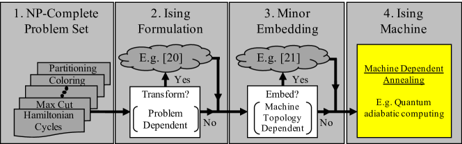
Because of the trivial mapping of the Max-Cut problem to the Ising formula, designers of Ising machines, often focus on this optimization problem. However, other optimization problems can also be mapped to an Ising machine. Indeed, every problem in the original NP-complete set (Miller et al., 1972) can be expressed by an Ising formulation specifically designed for that problem (Lucas, 2014). Note that Ising formulation may require more nodes than that of the original formulation and usually requires additional time to compute coupling coefficients in the Ising formulation from the original formulation. This transformation is largely straightforward and the need for it is problem-dependent and thus shared by all Ising machines.
Another transformation, however, may be necessary depending on the machine’s coupling topology. While we will get into the details as we discuss the machines, it is worth emphasising up front the significant impact of the issue. If a machine does not have all-to-all connections between physical nodes, two coupled logical nodes may be mapped to physical nodes (call them and ) not directly connected. As a result, additional auxiliary physical nodes are needed, through which nodes and are eventually connected. An alternative description is that if a machine has a limited connection topology, then the graph of a problem needs to be transformed (e.g., using minor embedding (Cai et al., 2014)) into a new graph that observes the limitation imposed by the machine. Consequently, a graph of size may contain many more nodes (e.g., ) after the transformation. Fig. 1 illustrates these transformations in the process of solving a problem on a generic Ising machine.
2.3. Quantum mechanical and optical Ising machines
There are many natural systems that can be described by the Ising model. We take two such existing systems for example. D-Wave’s quantum annealers use superconducting qubits as the basic building block. These bits are then coupled together with couplers forming a connection topology known as the Chimera graph. This is an important architectural constraint that limits the topology of the problem that can be mapped to the machine. As we will see later, despite supporting nominally more than 2000 spins, many of our benchmarks can not be mapped to the machine. Another disadvantage of the system is the cryogenic operating condition (15mK) needed for the quantum annealer. This requirement consumes a significant portion of the 25KW power of the machine (D-Wave, 2020).
Coherent Ising machines (CIMs) are another recent example of Ising sampling machines (Inagaki et al., 2016; Yamamoto et al., 2017; McMahon et al., 2016; Takata et al., 2016; Böhm et al., 2019). In a CIM, an optical device called OPO (optical parametric oscillator) is used to generate and manipulate the signal to represent one spin. Unlike in a D-Wave Ising machine, the coupling between spins in CIM is relatively straightforward in principle. As a result, CIM implementations have always supported all-to-all coupling. The authors also emphasized that the 2000-node CIM is therefore far more capable than D-Wave 2000Q which can only map problems of size 64 (Hamerly et al., 2019).
CIM is not without its disadvantages. To support 2000 spins, kilometers of fibers are needed. Temperature stability of the system is thus an acute engineering challenge. Efforts to scale beyond the currently achieved size (of about 2000) have not been successful as the system runs into stability problems. Also worth noting is that the coupling between nodes is – at least in the current incarnation – implemented via computation external to the optical cavity. There is a rather intensive computational demand (100s of GFLOPS) (Takesue et al., 2019). Every pulse’s amplitude and phase are detected and its interaction with all other pulses calculated on an auxiliary computer (FPGA). The computation is then used to modulate new pulses that are injected back into the cavity. Strictly speaking, the current implementation is a nature-simulation hybrid Ising machine. Thus, beyond the challenge of constructing the cavity, CIM also requires a significant supporting structure that involves fast conversions between optical and electrical signals.
These room-sized Ising machines are certainly worthwhile creations for the sake of science. In particular, investigations are needed to see whether the theoretical underpinning for these machines is relevant in practice. As we shall see later, both models have significant room for improvements.
2.4. Electronic oscillator-based Ising machines
A network of coupled oscillators is another physical implementation of an Ising machine. After sufficient time, the coupled oscillators will synchronize forming stable relative phase relationship.444The observation of such synchronization dates back to at least the 17th century when Huygens observed synchronization of two pendulums (Rosenblum et al., 1996). Synchronization phenomenon is the subject of research efforts in a wide variety of fields. Large-scale synchronization of firefly flashings and rhythmic applause in a large crowd of audiences are but two examples in the general underlying principles beyond mechanical objects. While many factors (e.g., amplitude, stochastic noise) will influence the phase of each oscillator, the following formula is a simplified steady-state description of phase relationship for oscillators:
| (5) |
Note that this simplified model ignores certain elements (e.g., diffusion due to noise) and is thus an approximation of a more complicated reality. Given such a differential equation describing a dynamic system, it can be shown that a Lyapunov function in the following form exists (Wang and Roychowdhury, 2019):
| (6) |
This means that the system will generally evolve along a trajectory that minimizes the Lyapunov function (Vidyasagar, 1978). As a result, the system’s stable states represent good solutions that minimize the right hand side of Eq. 6. On a closer inspection, we see the resemblance of Eq. 6 and the Ising model (Eq. 2). Specifically, when all phases () are either 0 or , the two formulae are the same.555In fact, the formulation of Eq. 6 is similar to the classic XY spin model (again ignoring external field): each spin can point to any direction along an “XY” plane and thus can be represented by a phase (). Ising model is thus a special case of the XY model. In other words, a system of coupled oscillators form an “XY machine” (not an Ising machine). An XY state can be quantized into an Ising state () in a number of different ways. For the sake of this paper, let us simply imagine direct quantization which rounds the phase to the nearest multiple of . A number of oscillator-based Ising machines have been recently proposed (Wang and Roychowdhury, 2019; Wang et al., 2019; Chou et al., 2019; Wang and Roychowdhury, 2017). All these examples use LC tank oscillators. While this is a common practice for analog circuit designers and relatively straightforward for discrete-element prototypes, the use of LC tanks introduce non-trivial practical challenges in integrated circuit (IC) designs. The lack of high quality inductors and the usually high area costs of incorporating them are common challenges for integrated RF circuitry. These desktop Ising machines are a significant improvement (at least in size) over room-sized Ising machines. But, for genuine wide-spread applications, we believe a clean-slate IC-focused design is a valuable direction to pursue. Needless to say, we believe there will be significant cross-pollination of different approaches and future practice may very well be a confluence of multiple styles of Ising machines.
2.5. Accelerated simulated annealing
Finally, a set of chips have been designed to accelerate simulated annealing (Kirkpatrick et al., 1983) or a variant of the classic algorithm. These chips are often described as having tens of thousands of spins (Yamaoka et al., 2015; Takemoto et al., 2019). In these designs, the spins are virtual in that they are bits in memory and manipulated by an algorithm (simulated annealing). These machines are specially built to accelerate that algorithm. Hence we refer to such a machine as an Accelerated Simulated Annealer or ASA for short.
These ASAs differ fundamentally from physical Ising machines. In a physical Ising machine, nature guides the spins to a preferable state according to physical laws. Thus, the machine can achieve ultimate speed and energy efficiency in principle – though it is entirely possible that a particular physics exploited is slow or energy-intensive to control; or it may be expensive to enable the physics, such as in creating the cryogenic environment required for quantum annealing.
2.6. Design space
Existing Ising machines can be placed in a design space along a number of dimensions. Fig. 2 visualizes this high-level classification.
The first dimension is whether they use physical or virtual spins. Note that this aspect is more of a continuum than a binary distinction. In the case of CIM, for instance, the interaction of the spins happens physically in the fiber. But the appropriate amplitude of feedback is controlled using external calculation.
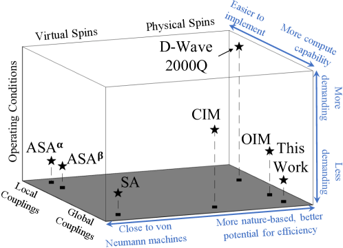
A second important differentiator of Ising machines is the connection topology. As discussed before, with a local connection, there is a limitation on the kind of problems that can be mapped to the machine. When a problem does not map directly, a transformation is needed to convert the problem, usually by requiring many auxiliary nodes. The nominal number of spins a machine provides is therefore a very poor representation of the machine’s capability. We will provide a quantitative analysis on this point in Sec. 4. At this point, we qualitatively place existing Ising machines based on their connection topology on one axis in Fig. 2.
Finally, a third dimension characterizes how demanding the operating conditions are. Nature-based computing is attractive for its potential in speed and energy efficiency. But in some cases, the physics that allows nature-based computing requires stringent operating conditions. D-Wave’s quantum annealers are one such example. Much of the system’s bulk and energy consumption is to create the cryogenic operating conditions for the system to work properly. Similarly, but to a lesser extent, CIM requires stringent temperature stability and noise isolation to ensure the stability of the interacting optical pulses. Electronic Ising machines, on the other hand, can operate in room temperature and are unlikely to require a special supporting environment. Nevertheless, similar to analog electronics, they will be more sensitive to noise than conventional digital computers. Later, we will show some analysis of our design’s behavior in a typical on-chip environment.
3. Design of the CMOS IC Ising Machines
In this section, we start with a simplified system to provide some intuition about how common electronics can also make a physical Ising machine (Sec. 3.1); then describe in more detail the system architecture (Sec. 3.2) and the design of key circuits (Sec. 3.3); and finally present theoretical analysis of the system’s optimum-seeking behavior (Sec. 3.4).
3.1. Overview & intuition
As already discussed before, existing physical Ising machine have different strengths and weaknesses. The room-sized machines are vehicles for continued scientific exploration of the underlying principles. It is particularly useful to show the difference between ideal theoretical capabilities and what can be achieved in practice. For instance, according to quantum adiabatic theory, the system’s Hamiltonian needs to be changed sufficiently slowly to guarantee that the system stays in ground state. Operated as such, the quantum annealer predictably provides sub-optimal solutions, as we will show later.
The question then becomes: can we build better (smaller, less power-intensive)
physical Ising machines. And the answer is: yes, with electronics. In digital
designs, electronic devices are often thought of as no more than the building
blocks of functional units. But their behavior is also subject to physical
laws that can be leveraged to perform nature-based computation. As it turns out,
practical physical Ising machines can be built out of common devices such as
capacitors and resistors. We start with one such simple design to show the
working principle. Of course, this design is not yet a high-performance system.
But as we will show later, with a proper architecture and careful design of key
elements, a physical Ising machine built out of electronics is much more compelling
than existing proposals. Additionally, it can be fabricated entirely in a CMOS
process.
Intuition: In the Ising model, when two nodes (say, , and ) are strongly and positively coupled (i.e., is large and positive), their spins are likely to be parallel (). In this way, the term will contribute to lowering the energy. Conversely, a strong negative coupling ( is large and negative) will likely lead to anti-parallel spins (). Finally, weak coupling ( is small) suggests that the two spins are more likely to be independent.
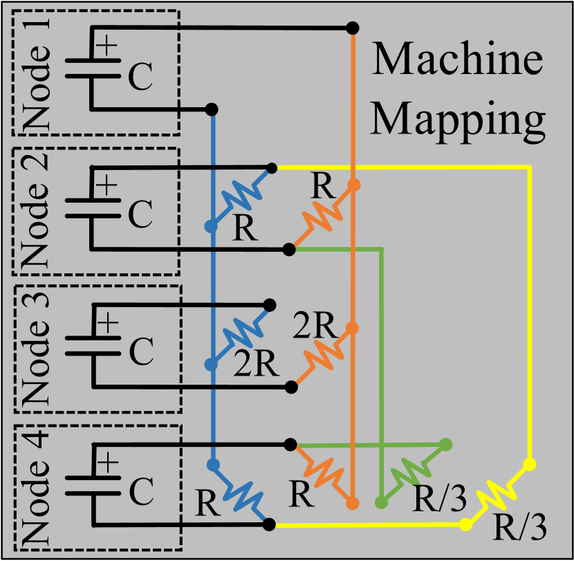
This behavior can be easily mimicked with resistively coupled capacitors. Consider representing a node with a capacitor, where the polarity of the voltage across it represents the spin of the node. More specifically, in Fig. 3, if a node has a spin of “-1”, the voltage at the upper terminal (top plate of the capacitor, labeled “+”) is lower than that of the lower terminal (bottom plate of the capacitor). We can then connect nodes with different resistors. A strong coupling means high conductance (or low resistance), so that voltages of two nodes can more easily equilibrate. So, we set . The sign of coupling can also be achieved by connecting either the same or opposite polarity terminals of the corresponding capacitors. Fig. 3 shows a simple 4-node system mapped from a logical graph of a Max-Cut problem with the labeled edge weights. 666Recall the coupling and edge weight relation, , in the Ising formula. It is not difficult to see that the solution should separate the nodes into and . Let’s see how the machine functions.
The graph translates to couplings in a straightforward manner: , where the sign indicates polarity of coupling. For instance, nodes 1 and 4 () are parallel/positively coupled (). So a resistor of connects the upper terminals of nodes 1 and 4 and another connects the two lower terminals. Nodes 1 and 3 () are antiparallel/negatively coupled (), so a resistor connects the upper terminal of Node 1 and the lower terminal of Node 3, and another resistor connects their remaining terminals.
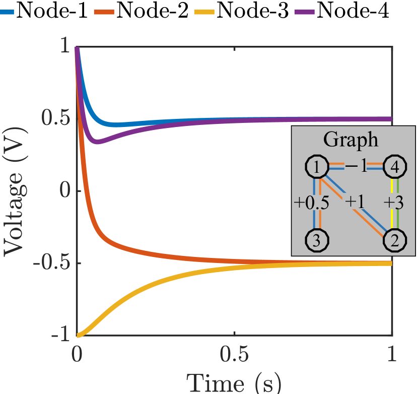
Once initialized with random polarities, these coupled capacitors can indeed seek some equilibrium as shown in Fig. 3 (right). In this example, the polarity of the capacitors at equilibrium indeed gives the best solution to the Max-Cut problem.
While this oversimplified design confirms the intuition that it can find a solution, it is far from a robust design. For example, depending on the initial state and system scale, the voltages at equilibrium can be or just too low for reliable readout. The equilibrium is also temporary because leakage will make all nodes decay to eventually, rather than staying at the desired voltage levels. Nevertheless, the resistively-coupled capacitor network is at the core of our proposed Ising machine. To induce and maintain the nodes at equilibrium, we can introduce a local feedback unit to make the node voltages bistable. For brevity, we will refer to such a Bistable, Resistively-coupled Ising Machine as BRIM.
3.2. Architecture of an integrated design
We now discuss the architecture of a more complete system designed for integrated circuits. The system is illustrated in Fig. 4 and consists of: ① bistable nodes (N1 to N4) and their digital interface (DFF 1-4); ② coupling units connecting the nodes (); ③ programming units to configure coupling weights (including: memory, multiplexers, digital-to-analog converters, and the column control systems); and ④ annealing control. We discuss each in turn as follows:
3.2.1. Nodes
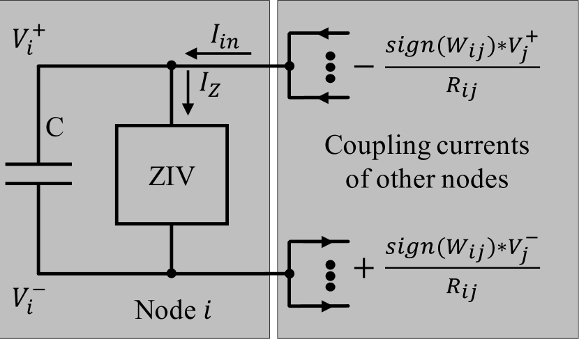
The bistable nodes are shown at the left side of Fig. 4. In Fig. 6, we show a more detailed illustration of one node. Recall that in the simplified circuit (Fig. 3) the capacitor’s voltage can be too low (even zero) as compared to electronic noise level to reliably indicate the node’s spin. A feedback circuit is therefore needed to stabilize the voltages at the desired levels (e.g., ). Two conditions are required: ① the capacitor should be charged according to its polarity when the voltage is between and , and discharged when the voltage exceeds this range; and ② at low voltages, the feedback circuit should supply a low current in order not to overwhelm signals coupled from other nodes.
Combining these considerations, we can design a feedback circuit with the current-voltage (IV) curve as shown in Fig. 6. Because of the slanted “Z” shape of the IV curve, we call such sub-system a ZIV diode. As seen in the IV curve, for capacitor voltages between and , the ZIV diode acts as an active element charging its voltage closer to . Conversely, for voltages outside the range, the ZIV diode acts essentially as a linear resistor to discharge the capacitor. Each node is supplied with two pairs of switches to set the capacitor voltage to a known spin state. This is useful for specific initialization or to change the system state as described in the “Annealing Control” (Sec. 3.2.4). Finally, the spin of the node can be read out by a digital latch (e.g., a D flip-flop) connected to the ZIV diode’s terminal. This converts the spin to a bit (1 or 0).
3.2.2. Coupling units
With an array of BRIM nodes, we have the flexibility to couple them in any desired topology. As we will discuss quantitatively later, an all-to-all coupling is computationally more useful and is thus our choice.
In our system, the coupling is (uni)directional. There are two separate coupling units (CU) connecting node to : and . This directional coupling is achieved by connecting the node capacitor through a voltage buffer before sending to the CU. The coupling coefficient of both directions are of course the same (). In principle, a bidirectional coupling has similar effects and is a simpler design point. But, empirically, we found directed coupling tends to produce better solution quality at the expense of area. A more detailed analysis as to the reason for this phenomenon is left as future work.
Because of the directed coupling scheme, each node has separate input and output terminals (two each for fully-differential coupling), as shown in different colors in Fig. 4. Similarly, each CU also has four input/output terminals, with one pair of transistors connecting the same polarity input/output nodes (parallel coupling) and another pair to establish anti-parallel coupling, as shown in Fig. 7.
The two pairs of transistors in the CU are biased in triode-region to act as variable/programmable resistors. Depending on the polarity of the coupling coefficient (), only one pair of the transistors are turned on and biased to an appropriate non-zero . For example, to establish a negative (anti-parallel) coupling, the gates of the upper-right and lower-left transistors are biased to a non-zero voltage (), while the other pair of transistors are biased at (GND).
3.2.3. Programming units
Both the initial nodal values and the coupling resistance are programmable. Programming of a resistor is achieved through a transistor with adjustable gate voltage. To the right of the coupling unit array in Fig. 4 is the programming array. This array consists of digital memory for storing the weights which drive an array of digital-to-analog converters (DACs). A small amount of such DACs are sufficient to program all the coupling units in a time-interleaved fashion per column. In such configuration, we need corresponding column selectors and pull-down logic as shown below the coupling units in Fig. 4.
3.2.4. Annealing control
With the basic network of coupled bistable nodes, the system can reach the local optimum determined by the initial state. Two commonly used mechanisms for annealers are incorporated to allow the system to escape local optima. First, the coupling strength is globally increased over time. In this way, at the very beginning, the machine is only weakly coupled, rendering the energy landscape relatively flat. This helps the system explore the landscape in a coarse granularity. We choose an exponential annealing schedule because (a) it is a common practice, and (b) it can be conveniently achieved by discharging an appropriately sized capacitor as the global annealing scheduler. The voltage from this capacitor is then used to control the variable gain buffer in each node to achieve the change in coupling strength.
Second, we also adopt a similar strategy as that used in simulated annealing. By performing a “spin flip” of select nodes (i.e., to change the spin to its opposite value), we can enter a neighboring state in the global phase space. This allows the system to escape the current basin of attraction and explore new regions. In simulated annealing, the probability of such bit flips is a function of both energy difference due to the bit flip and the current temperature. For implementation convenience, we only use the temperature to decide the probability/frequency of spin flips. The temperature follows the same exponential annealing schedule discussed above. In other words, the frequency of spin flips decays exponentially. When a spin flip is decided, we randomly select a node and use the switches shown in Fig. 6 to achieve the purpose.
With these supports, our BRIM is used similarly to other Ising machines: first, program the weights; then, select the annealing time; and finally, read out the state of the nodes after the completion of the annealing schedule. Note that the system can be used in a number of different ways: the annealing time can be adjusted; the spin flip frequency can be tuned; the machine can also be used together with a software-based search algorithm (e.g., simulated annealing), perhaps by searching a subspace.
3.3. Integrated circuit design
Fig. 8 shows the circuit of a BRIM node. The design is fully balanced, and can therefore be understood by analyzing either half. The circuit can be understood as the following functional blocks:
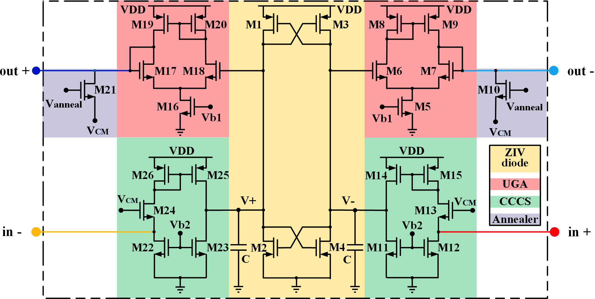
-
(1)
Bi-stable node: Transistors to (center) are an integrated realization of the ZIV diode. It captures the overall IV characteristic shown in Fig. 6 with a very simple circuitry, namely, two cross-coupled inverters. Together with capacitors connected on both sides of the ZIV diode, the core of the node with a bi-stable state is formed. The rest of the node is the interface to the coupling units.
-
(2)
Output buffer: Recall that the voltage of the node goes through a buffer before being connected to the coupling units. This buffer is implemented by transistors to (top right) which form a single-ended differential amplifier configured in what is called a unity-gain topology. The gain of the buffer changes with annealing – as we will show later – making it a Unity Gain Amplifier (UGA).
-
(3)
Input current control: The current from coupling units goes through a current-controlled current source (CCCS) to connect to the nodal capacitor. Transistors to (bottom right) compose an integrated CCCS, which is modified from an active cascode summing circuit (Comer et al., 2003).
-
(4)
Annealing control: operates as a variable resistor when applying an annealing voltage to its gate. is a global control signal supplied to all nodes according to a specific annealing schedule (e.g., exponential decay). At the onset of the annealing process, is set to which effectively shorts the output from the UGA setting its gain to and disconnecting the node from the coupling network. As continues to decrease following an annealing schedule, the channel resistance of increases resulting in a reduced loading to the UGA and a gradual increase in its gain. At the completion of the annealing schedule, the is fully off, the UGA’s gain is at its maximum value (about in our setup) and the node is fully connected to the coupling network.
-
(5)
Coupling resistors: The coupling resistors (from Fig. 7) are implemented as bootstrap switches/transistors commonly used in low-voltage switched-capacitor analog circuits. The parasitic capacitance of the bootstrap transistors is used to store and maintain the biasing voltage set by the low-level DAC during programming. This voltage regulates the channel resistance of the transistors.
3.4. Theoretical analysis
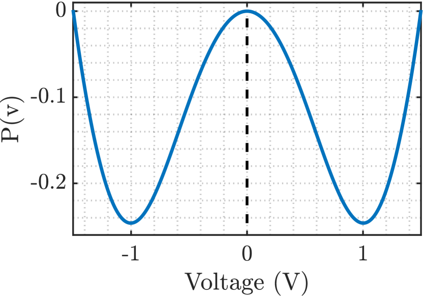
It is often desirable to show some theoretical foundation for nature-based computing machines. We present a Lyapunov stability analysis of BRIM to show its ability for optimum-seeking. Fig. 10 shows a simplified node in BRIM where other nodes are coupled into from the right. Writing the current equation, we get Eq. 7, where is the effective conductance of the coupling taking into account the polarity of the coupling:
| (7) |
BRIM is a continuous time system where the state is summarized by . (For brevity, in the following, will be abbreviated as .) Recall that in Lyapunov analysis, if a function can be found such that at point and in the region around , then is the equilibrium point (Vidyasagar, 1978). In our case, this point is the solution to the equation set .
In other words, once the system enters a region, it will inevitably evolve towards lowering (because its time derivative is negative) until it reaches the equilibrium point .
To ensure is non-positive, we can construct it to be in a negative square form. This can be achieved by imposing the following construction rule.
| (8) |
Following the chain rule, it is not difficult to see that:
| (9) |
One choice of a Lyapunov function satisfying the conditions in Eq. 8 is shown in Eq. 10, where is obtained from by integration over .
| (10) |
It is important to notice that the “Z” shape of will give a double-well profile (as shown in Fig. 10) with two stable equilibrium points at voltages corresponding to two non-trivial zero-crossings of the IV curve (e.g., ) and a saddle point at . Given the double-well profile of , the state of a stable solution will consist of voltages at (or at least very close to) these equilibria (e.g., ). Thus, the second term of Eq. 10 will be (close to) a constant. Consequently, minimizing is equal to minimizing the first term , which is the Ising formula.
Note that this analysis does not guarantee that the system will converge to a global minimum as it depends on the energy landscape and initial conditions. This is similar to other annealers: None has strong guarantees for reaching ground state in a typical usage scenario (as opposed to ideal conditions) or in an efficient manner. For example, it is shown that simulated annealing can reach ground state in a system with a finite phase space. However, the time it takes to do so may be longer than enumerating the space (Varty, 2017).
4. Experimental Analysis
In this section, we provide some experimental analysis of BRIM by
First, we describe the machines (Sec. 4.1), the benchmarks (Sec. 4.2) used in the analyses, and sample BRIM modeling (Sec. 4.3).
4.1. Ising machines
We compare a simulation based model of BRIM to 4 other machines using both physical and virtual spins. We use results reported in literature when direct measurement or modeling is unavailable.
-
(1)
D-Wave: we use 2000Q which is the latest quantum annealer (Harris et al., 2010) at the time of this documentation. We run jobs using the API provided by D-Wave (dwave-system, 2020). For each graph problem, we collect 50 samples. 777In terms of timing, we do not specify any constraints, and adopt D-Wave default values. Specifically: , , , and respectively for annealing, data readout, inter-sample delay, and programming time (dwave qpu time, 2020).
-
(2)
CIM: is an optical Coherent Ising Machine (Inagaki et al., 2016). There is no known public access to the actual hardware and no model available for simulation. Thankfully, there are reported results for two commonly used benchmarks and a 2000-node complete graph that allow us to make meaningful comparisons.
- (3)
-
(4)
ASA: refers to a number of related designs of Accelerated Simulated Annealers (Yamaoka et al., 2015; Takemoto et al., 2019). These accelerators use virtual spins and are straightforward to model based on the description in literature. We focus on one with 30,000 nominal spins. In this design, the coupling follows a near-neighbor pattern dubbed the King’s graph. All nodes are grouped into 4 groups. For every annealing step (), nodes in one of the groups will process in parallel: they read off neighbors’ spins and the associated weights to compute whether keeping the same spin or inverting its current spin provides a lower energy in the neighborhood. In addition, random bit flips similar to those in standard simulated annealing algorithms are also adopted.
As explained in Sec. 2 (box 3 of Fig. 1), machines without all-to-all coupling (D-Wave and ASA) require preprocessing of input graph through minor embedding (Cai et al., 2014). This process currently takes significant time on a conventional computer (more details in Sec. 4.5) and can often fail for larger graphs. ASA uses the King’s graph which is even more limited than the Chimera graph in D-Wave, the minor embedding process takes even longer time to complete and results in more physical nodes needed. In our high-level analysis, we ignore the significant time needed for this preprocessing.
Finally, we also added an optimized version of the Simulated Annealing (SA) (Isakov et al., 2015) algorithm as a reference written in C++. The execution time is measured on server cluster nodes of Intel Xeon Platinum 8268 CPUs at 2.9GHz with 371GB of RAM.
4.2. Benchmarks
To compare these systems, we use a set of popular graphs called “Gset” (and their derivatives) with diverse node sizes and edge densities. These graphs are just weighted, undirected graphs and not associated with any specific problem. They naturally correspond to an Ising formula. Thus, we are comparing different machines optimizing the same set of Ising formulae.
Because of the direct mapping between an Ising formula and the Max-Cut problem, and that many algorithms have been developed for optimizing Max-Cut, it is convenient for researchers, especially Ising machine designers, to interpret these graphs as specifying a Max-Cut problem, which we follow in this paper. Note that this does not mean we can only solve a Max-Cut problem as already discussed in Sec. 2.
The graphs we use can be divided into the following groups:
-
(1)
Regular graphs: We use the original Gset graphs from Stanford (Ye, [n.d.]). These graphs have between 800 and 20,000 nodes. The edges as well as the weights of such edges, were generated probabilistically, sometimes between +1 and -1, and sometimes all +1. We only use those graphs with less than 2000 nodes in our experiments.
-
(2)
Tiny graphs: Finally, we also generated fully-connected graphs with random edge weights, and node sizes ranging from 16 to 32 (in increments of 4). Each node size has 20 sample graphs, for a total of 100 graphs. For these graphs, we are able to enumerate all possible spin combinations to determine the actual maximum cut.
4.3. BRIM sample modeling
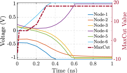
We demonstrate an example model of the continuous-time BRIM system before getting to detailed analysis of the diverse machines. In this example, we use MATLAB’s nonstiff, single step, 5th-order differential solver (ode45). Listing 1 shows the sample BRIM implementation of Eq. 7. In listing 2, we demonstrate the setup and test for solving a simple 6-node David-graph problem the sample BRIM machine. Fig. 11 shows a sample voltage transition of each node in the BRIM system.
|
1function dvdt = brim(~, v, W)
2 C = 49e-15; % Node capacitor
3 Rc = 31e3; % Coupling resistor
4 ziv = @(v)(-2.1563e-05 .* v.^5) + ... % Diode
5 ( 1.017e-04 .* v.^3) + ... % ...
6 ( -2.231e-05 .* v); % ...
7
8 J = -W ./ Rc; % Ising transformation
9
10 dvdt = ((J * v) - ziv(v)) ./ C; % BRIM expression
11
12 dvdt((v < -1) & (dvdt < 0)) = 0; % Model diode range
13 dvdt((v > 1) & (dvdt > 0)) = 0; % ...
14end
|
|
1function sample
2 % David-graph problem with maximum cut value of 18.2
3 src = [1 1 1 1 2.0 2 2.0 3 3.0 4 4 5.0];
4 dst = [2 3 5 6 3.0 4 6.0 4 5.0 5 6 6.0];
5 wgt = [1 -1 -2 6 -0.2 -2 4.4 4 -4.4 6 -1 -0.2];
6
7 spin= length(unique([src dst]));
8 W1 = sparse(src, dst, wgt, spin, spin);
9 W2 = sparse(dst, src, wgt, spin, spin);
10 W = full(W1 + W2);
11
12 % Solve BRIM system
13 F = @(t,v)brim(t, v, W); % Work function
14 T = [0 1e-9]; % Annealing time
15 I = rand(spin, 1) - 0.5; % Initial states
16 sol = ode45(F, T, I); % Solver
17
18 % Display solution
19 plot(sol.x, sol.y);
20end
|
4.4. High-level comparison
It is important to keep in mind that Ising machines are far from mature. Early designs and prototypes are necessarily experimental in nature and thus lack the polish of, say, a classical computer architecture. Much of the performance difference may be due to the art of prototyping rather than the fundamental science of the mechanism being exploited. This is perhaps especially the case for D-Wave, as in our comparison, it is the only actual hardware that we have access to. (CIM and OIM both have hardware prototypes but are not accessible to us.)
We start with a crude, high-level comparison of different Ising machines. There are several practical factors that make this comparison crude and incomplete. First, there is no single problem that can be measured on all machines. This is primarily because CIM only reported raw data on a very specific set of benchmarks and we are unaware of any reliable model of the physics that is publicly available. Second, the workload of optimization usually allows tradeoff between speed and quality of the solution. Ideally, we will fix one metric (say, execution time) and compare the other (quality of solution). But in some cases, such control is unavailable to us. Third, the execution result depends on initial conditions. So any single run is subject to random chances. The common practice of using these machines is doing multiple runs and taking the best solution, which we follow. But this value should still be regarded as a random variable.
4.4.1. Area and power estimates
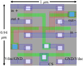
We use reported D-Wave and ASA power numbers from literature. Due to the nature of the underlying physics being exploited, it is unlikely for these machines to reach chip-level size in the near future, if ever. For BRIM, we envision an integrated circuit implementation. For a rough sense of the product, we perform a preliminary design and layout of components in Cadence using generic 45 nm PDK. For BRIM, the area will be dominated by the 4 million coupling units (CU). As can be seen in the layout shown in Fig. 12, one coupling unit takes about . Additionally, a BRIM node has the size () and a DAC for the weights is (). Combined, the rest of the system outside the coupling network will be less than 1% total area and even less in larger systems.
Power consumption was collected in Cadence modeling a 6-node system (Fig. 18) and measures . Since the Gsets tested (Table 1) are all sparse (with 16.4 edges/node ratio), we simply extrapolated to for 2000-nodes for a coarse grain, order-of-magnitude estimate. A simplified first-principle calculation shows the power to be .
4.4.2. Sample 2000-spin machine
With these caveats in mind, Table 1 shows high-level metrics; the estimated power and chip area (when applicable), the execution time (machine annealing time), and solution quality of sample designs with 2000-spins. The cut value itself changes a lot: some graphs have a cut value around 100, others around 2000. A better measure of solution quality is thus not the absolute cut value, but the distance (how close the solution is) to the best known cut value in literature.
| Parameters | |
|---|---|
| Power (W) | |
| Area () | |
| Effective Spins | |
| G22 | Distance |
| Time | |
| G39 | Distance |
| Time | |
| K2000 | Distance |
| Time | |
| CIM | OIM | ASAU | SA | BRIM |
| unlimited | ||||
-
(1)
CIM comparision: We use CIM running graphs G22, G39, and K2000 as baseline because these are tested on CIM and reported (Fig. 3 of reference (Inagaki et al., 2016)). These graphs cannot be mapped on D-Wave. For other machines, we try to match CIM’s solution quality and show execution time. We see that BRIM can obtain similar quality solutions 4 orders of magnitude faster with a power consumption about 3 orders of magnitude better.
-
(2)
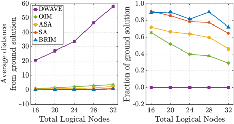
Tiny graph comparison: Recall that for these graphs we know the ground state solution from enumeration, and we verify that BRIM, OIM, and ASAU can reach the ground state. Yet, even for these tiny graphs, D-Wave does not reach the ground state, with the best solution having an average distance of 20. A more detailed view of the solution quality can be seen in Fig. 13 showing average solutions and probabilities of going to the ground state. SA and BRIM can both achieve ground state often. But BRIM can do so with higher probability. These are concrete examples where the theoretical ability to reach the ground state for an Ising machine is just that: a theoretical ability.
-
(3)
To sum: We see that the room-sized machines (CIM and D-Wave) do not show any tangible advantage in solving our weighted Max-Cut optimization problems. D-Wave can only map the smaller problems due to the connection limits. Even on these smaller problems, its solution quality trails behind others. Recall this limited connection means additional compute time to perform minor embedding, which at the moment takes , on average. CIM is less power-hungry and can map bigger problems due to its all-to-all connections. Nevertheless, there is no tangible advantage in any figure of merit. Again, these machines may (or may not) prove useful for scientific exploration and may (or may not) show some qualitative superiority at some other scale or at a future time.
The most important take-away point is that just because the machine leverages nature to perform computation does not necessarily make it efficient. Much engineering diligence is needed to convert some theoretical possibilities to tangible practical benefits.
4.4.3. Electronic designs
Next, we look at the electronic designs. While the current OIM prototype is a desktop machine, in principle it can be scaled down in size and up in frequency. The primary unknown is to what extent the nodes can scale down and still operate like ideal LC-tanks. For this study, we assume a 100MHz frequency. Admittedly, this is nothing more than a rough guess. We see that OIM is perhaps comparable to BRIM, though subjectively, we feel that the practical challenges are far more daunting than in BRIM.
We also compare ASA with BRIM. ASA is essentially a specialized computer doing algorithmic search for better cut values. Clearly, ASA takes advantage of the tremendous cumulative improvements of CMOS technology to provide relatively fast and efficient computation. However, it is still a modified von-Neumann machine (with its only program hardwired). In contrast, BRIM is a physical Ising machine where nature is performing the computation. Indeed, here, we see that to get similar quality solutions on small graphs, BRIM is still producing better results while consuming a tenth of the power, with a 5x lower area cost, and providing 12x more spins. It is tempting to think that the area comparison is unfair because ASA offers a large number of nominal spins. We will show next that the nominal number of spins is an extremely poor, if not useless, metric.
Finally, the last column shows the result of a conventional computer running simulated annealing for reference. We can clearly see the potential benefit of a high-performance Ising machine: we can obtain a speedup of about 7-8 orders of magnitude.
4.4.4. Recap
We see that: ① Ising machines can provide extraordinary speedups in certain types of problems; ② but for the scale of problems we are discussing, room-sized machines are not advantageous; ③ ASA, OIM, and BRIM are three possible candidates for chip-scale applications with perhaps different strengths. We look at these models in more detail next.
4.5. Detailed analyses
4.5.1. The impact of topology
We hope by now it is starting to be clear that BRIM is a compelling design. Next, we want to get into details to understand some of the intrinsic strengths that made it a compelling design. We first discuss an important issue in Ising machine architecture. As already mentioned, when an Ising machine uses a more local coupling network, it has a more limited ability to map problems. Many problems would need far more physical nodes than logical nodes in the problem. To show this, we create a number of small graphs with edge density of 6%.
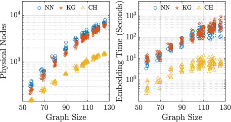
As shown in Fig. 14, even with these sparse graphs, it takes about 1600 nodes (in D-Wave’s Chimera configuration) to map a problem of size 126. Moreover, many nominally unused spins cannot be used due to their location. In fact, no size 127 problems we tried can be mapped to the 2048 nominal nodes. To map these graphs, it takes up to 10 seconds to carry out the minor embedding algorithm for Chimera. For ASA’s nearest-neighbor or King’s graph topologies, the problem is more pronounced. To map the same 126-node graph, it takes up to 8031/6649 physical nodes respectively and 500s/955s of execution time respectively. Note that the preprocessing time is orders of magnitude longer than the annealing process itself and more than needed to get a better solution using conventional simulated annealing. Finally, auxiliary spins degrade the machine’s ability to find good solutions. As we saw in Table 1, D-Wave and ASA have trouble reaching the ground state for small graphs. All in all, at the moment, we see no evidence that using local connections (at least these specific ones) is helpful in any practical way.
4.5.2. In-depth comparison
Next, we study the annealing process for BRIM, ASA, and OIM more in-depth. In Fig. 15, we show the solution quality (measured as distance from best known solution) as different machines are given different annealing time. We add simulated annealing (SA) running on a workstation to this mix. Each marker’s vertical coordinate represents the difference between the best solution and the final cut value (lower is better), while its horizontal coordinate shows the annealing time. The range of annealing times are chosen such that the quality of the solution fits into roughly the same band.888 Note that each additional dot to the right takes 10x longer to obtain.
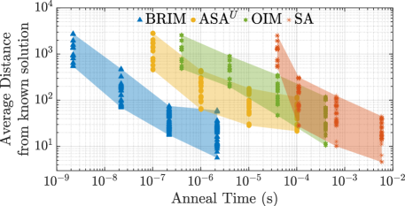
An important point needs to be made about ASA. We create an idealized model where it supports all-to-all connection and can update all nodes within a cohort sequentially in one annealing step. Note that this is intended as a very loose upper-bound of performance for the same kind of machine, and labeled as in Fig. 15.
We can see the general trend that a longer annealing time provides a better answer for all machines. It is also clear that BRIM is orders of magnitude faster than other systems. However, rather than thinking about these curves as fixed and precise, it is helpful to think about them as a general shape that can move horizontally. Their position only represents the effect of current design parameters. And it is instructive to understand what it takes to move them to the left by, say, one order of magnitude. For ASA and SA, this is equivalent to making the machine 10x faster. We can imagine the challenge of this given the difficulty of scaling computation speed, not to mention memory access time. For the analog implementations, the question is more subtle. By reducing capacitance and/or inductance, the curve can shift to the left. The real question becomes the impact of noise and parasitics both to speed and solution quality. Such investigation is part of our future work.
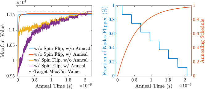
4.5.3. Effects of annealing control
As already mentioned earlier, this paper highlights a different approach to Ising machine. The specific example used so far is but one design point in the space and much of the space remains to be explored in more detail. For example, annealing control plays a crucial role in obtaining good solutions. Fig. 16 compares the system with a few different configurations aiming at achieving better results. For example, we can exponentially adjust the coupling strength over time. This allows the system to navigate the landscape at a coarser granularity early on. Additionally, we can periodically and randomly reverse the polarity of some nodes (to apply random spin flips) to escape a local minimum. On the left, we show the effect of applying spin flips and coupling strength annealing. We find that applying random spin flips are indeed very effective as expected.999Instead of adding completely random spin flips, we also studied another approach in simulation. In this approach, the energy values of the current state and destination state are calculated and whether the destination state is accepted depends on the energy values as in a Metropolis–Hastings algorithm. We note that this approach does offer better results though it is challenging to implement in hardware.
4.5.4. Effects of bit precision in coupling control
Since BRIM uses a number of analog circuits, it is natural to be concerned about the impact of noise and other non-idealities on its operation. Building and testing actual hardware will be the ultimate experiment to answer those concerns. But a number of simulation-based experiments can still shed some light. We first look at whether we can provide enough precision in programming the coupling weights.
To answer the question, we compare BRIM with different bit precisions in the weight matrix. The Gset benchmarks actually have weights of . So for this experiment, We introduce a hypothetical problem with real coupling weights uniformly distributed in [-1, 1]. We then set the programming system including DAC to support 6 to 12 bits of precision and compare the result to the reference of supporting single-precision floating point weights. Fig. 17 shows the range of the solution on the left and the average probability of achieving ground state solution on the right.
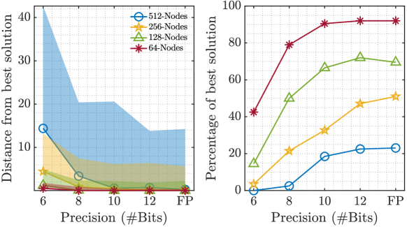
We can see that dropping weight precision from single-precision FP to 12 bits has virtually no impact in any respect. Further reducing the precision will bring some noticeable impact, with 6 bits being on the boundary of acceptability. Keep in mind, such uniformly distributed weights represent perhaps the extreme of demand on weight precision.
4.5.5. Effects of variation and noise
To evaluate the effect of device variations we introduced mismatch to coupling resistors (), buffer gain (), and buffer offset () drawn from normal distribution. Additionally, we also introduced electronic noise () to the output of every node over the entire annealing process. The magnitude and variation of the noise are obtained from circuit simulation by integrating the output noise at and of Fig 7 from within the bandwidth of the voltage buffer (1Hz to 100MHz). Overall, the impact of noise and variation is rather tolerable. This can be seen by the average distance to the best solution. Without variation and noise, the distance is 3.8. Accounting for device variations increases the distance to 4.2. Adding noise, with or without variations, increases the distance to 5.
4.6. Discrete-component prototype
We now showcase a limited prototype of BRIM using discrete electronics with operational amplifiers and passive components such as capacitors as well as resistors. The prototype is meant to demonstrate the key operation principle and therefore does not have some features such as programming interface and advanced annealing control to escape local minima.
The six nodes are implemented each with a capacitor and a ZIV diode made out of an op-amp. These are seen in the bottom right of Fig. 18. The coupling can be seen above the nodes in the figure. In this prototype, the nodes are directly connected with resistors without any buffer. Thus the coupling is bidirectional.
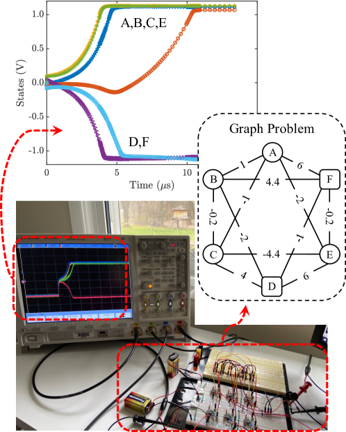
There is no state initialization in this prototype and each node starts at a voltage of 0. Noise intrinsic to the setup helps each node break out of the saddle point () and bifurcate to one of the stable states of determined by the specific set up of the ZIV diodes. Each run from power-up thus gives a different waveform on the scope and a potentially different solution. A waveform from simulation as well as the waveform on the scope can be see in Fig. 18. In this particular setup, the energy landscape is relatively simple and the prototype always reaches the ground state.
5. Conclusions
Ising machines can be programmed to map an abstract problem and let physics naturally guide the dynamical system towards some kind of optimal state. This state can then be translated back to be a heuristic solution to a combinatorial optimization problem. The use of nature suggests the possibility of significant speed and/or efficiency. Consequently, exploration of Ising machines has been gaining attentions. Quantum annealers and optical coherent Ising machines are prominent examples of such machines which drew particular interests from the physics community. However, these Ising machines are generally bulky and energy intensive. Continued exploration is certainly a worthwhile endeavor for scientific purposes. But for now, integrated circuit designs allow more immediate applications. We propose one such design we call BRIM that uses bistable nodes resistively coupled with programmable and variable strengths. The design is fully CMOS compatible for chip-scale implementations. Through our experimental analysis, we show that the machine is significantly smaller, faster, and more energy-efficient relative to some other designs. Compared to the room-sized Ising machines, it is about 4 orders of magnitude faster and consuming 7-8 orders of magnitude less energy. Compared to a recent chip-scale simulated annealing accelerator, it is also orders of magnitude better in speed, area, and power. While there is some degree of uncertainty with these statistics, we also envision continued improvement and optimizations. On the other hand, there are also many challenges facing machines like BRIM. Scalable architecture, area-efficient connection networks, and circuit scaling in the presence of Process-Voltage-Temperature (PVT) variations are but a few examples of the challenges.
References
- (1)
- Böhm et al. (2019) Fabian Böhm, Guy Verschaffelt, and Guy Van der Sande. 2019. A poor man’s coherent Ising machine based on opto-electronic feedback systems for solving optimization problems. Nature Communications 10, 1 (2019), 3538. https://doi.org/10.1038/s41467-019-11484-3
- Boixo et al. (2018) Sergio Boixo, Sergei V. Isakov, Vadim N. Smelyanskiy, Ryan Babbush, Nan Ding, Zhang Jiang, Michael J. Bremner, John M. Martinis, and Hartmut Neven. 2018. Characterizing quantum supremacy in near-term devices. Nature Physics 14, 6 (2018), 595–600. https://doi.org/10.1038/s41567-018-0124-x
- Bunyk et al. (2014) P. I. Bunyk, E. M. Hoskinson, M. W. Johnson, E. Tolkacheva, F. Altomare, A. J. Berkley, R. Harris, J. P. Hilton, T. Lanting, A. J. Przybysz, and J. Whittaker. 2014. Architectural Considerations in the Design of a Superconducting Quantum Annealing Processor. IEEE Transactions on Applied Superconductivity 24, 4 (2014), 1–10.
- Cai et al. (2014) Jun Cai, William G. Macready, and Aidan Roy. 2014. A practical heuristic for finding graph minors. arXiv:1406.2741 [quant-ph]
- Chen et al. (2014) Y. Chen, T. Luo, S. Liu, S. Zhang, L. He, J. Wang, L. Li, T. Chen, Z. Xu, N. Sun, and O. Temam. 2014. DaDianNao: A Machine-Learning Supercomputer. In 2014 47th Annual IEEE/ACM International Symposium on Microarchitecture. 2014 47th Annual IEEE/ACM International Symposium on Microarchitecture, micro, 609–622. https://doi.org/10.1109/MICRO.2014.58
- Chou et al. (2019) Jeffrey Chou, Suraj Bramhavar, Siddhartha Ghosh, and William Herzog. 2019. Analog Coupled Oscillator Based Weighted Ising Machine. Scientific Reports 9, 1 (2019), 14786. https://doi.org/10.1038/s41598-019-49699-5
- Comer et al. (2003) David J Comer, Donald T Comer, Aaron K Martin, and James E Jaussi. 2003. A high-frequency CMOS current summing circuit. Analog Integrated Circuits and Signal Processing 36, 3 (2003), 215–220.
- D-Wave (2020) D-Wave. 2020. The D-Wave 2000Q Quantum Computer. {https://www.dwavesys.com/sites/default/files/Dwave_Tech%20Overview2_F.pdf} Accessed: 2020-04-13.
- Dutta et al. (2019) S. Dutta, A. Khanna, J. Gomez, K. Ni, Z. Toroczkai, and S. Datta. 2019. Experimental Demonstration of Phase Transition Nano-Oscillator Based Ising Machine. In 2019 IEEE International Electron Devices Meeting (IEDM). IEDM, IEDM, 37.8.1–37.8.4. https://doi.org/10.1109/IEDM19573.2019.8993460
- dwave qpu time (2020) dwave 2020. Breakdown of QPU Access Time. dwave. {https://docs.dwavesys.com/docs/latest/timing_qa_cycle_time.html} Accessed: 2020-04-13.
- dwave-system (2020) dwave 2020. dwave-system. dwave. {https://docs.ocean.dwavesys.com/en/stable/getting_started.html} Accessed: 2020-04-13.
- Erbagci et al. (2015) B. Erbagci, N. E. C. Akkaya, C. Teegarden, and K. Mai. 2015. A 275 Gbps AES encryption accelerator using ROM-based S-boxes in 65nm. In 2015 IEEE Custom Integrated Circuits Conference (CICC). CICC, CICC, 1–4. https://doi.org/10.1109/CICC.2015.7338448
- Hamerly et al. (2019) Ryan Hamerly, Takahiro Inagaki, Peter Leonard McMahon, Davide Venturelli, Alireza Marandi, Tatsuhiro Onodera, Edwin Ng, Carsten Langrock, Kensuke Inaba, Toshimori Honjo, Koji Enbutsu, Takeshi Umeki, Ryoichi Kasahara, Shoko Utsunomiya, Satoshi Kako, Ken ichi Kawarabayashi, Robert L. Byer, Martin M. Fejer, Hideo Mabuchi, Dirk Englund, Eleanor G. Rieffel, Hiroki Takesue, and Yusaku Yamamoto. 2019. Experimental investigation of performance differences between coherent Ising machines and a quantum annealer. In Science advances. science advances, science advances.
- Harris et al. (2010) R. Harris, M. W. Johnson, T. Lanting, A. J. Berkley, J. Johansson, P. Bunyk, E. Tolkacheva, E. Ladizinsky, N. Ladizinsky, T. Oh, F. Cioata, I. Perminov, P. Spear, C. Enderud, C. Rich, S. Uchaikin, M. C. Thom, E. M. Chapple, J. Wang, B. Wilson, M. H. S. Amin, N. Dickson, K. Karimi, B. Macready, C. J. S. Truncik, and G. Rose. 2010. Experimental investigation of an eight-qubit unit cell in a superconducting optimization processor. Phys. Rev. B 82 (Jul 2010), 024511. Issue 2. https://doi.org/10.1103/PhysRevB.82.024511
- Inagaki et al. (2016) Takahiro Inagaki, Yoshitaka Haribara, Koji Igarashi, Tomohiro Sonobe, Shuhei Tamate, Toshimori Honjo, Alireza Marandi, Peter L. McMahon, Takeshi Umeki, Koji Enbutsu, Osamu Tadanaga, Hirokazu Takenouchi, Kazuyuki Aihara, Ken-ichi Kawarabayashi, Kyo Inoue, Shoko Utsunomiya, and Hiroki Takesue. 2016. A coherent Ising machine for 2000-node optimization problems. Science 354, 6312 (2016), 603–606. https://doi.org/10.1126/science.aah4243 arXiv:https://science.sciencemag.org/content/354/6312/603.full.pdf
- Isakov et al. (2015) S.V. Isakov, I.N. Zintchenko, T.F. Rønnow, and M. Troyer. 2015. Optimised simulated annealing for Ising spin glasses. Computer Physics Communications 192 (Jul 2015), 265–271. https://doi.org/10.1016/j.cpc.2015.02.015
- Johnson et al. (2010) C. Johnson, D. H. Allen, J. Brown, S. Vanderwiel, R. Hoover, H. Achilles, C. Cher, G. A. May, H. Franke, J. Xenedis, and C. Basso. 2010. A wire-speed powerTM processor: 2.3GHz 45nm SOI with 16 cores and 64 threads. In 2010 IEEE International Solid-State Circuits Conference - (ISSCC). ISSCC, ISSCC, 104–105.
- Jouppi et al. (2017) Norman P. Jouppi, Cliff Young, Nishant Patil, David Patterson, Gaurav Agrawal, Raminder Bajwa, Sarah Bates, Suresh Bhatia, Nan Boden, Al Borchers, Rick Boyle, Pierre-luc Cantin, Clifford Chao, Chris Clark, Jeremy Coriell, Mike Daley, Matt Dau, Jeffrey Dean, Ben Gelb, Tara Vazir Ghaemmaghami, Rajendra Gottipati, William Gulland, Robert Hagmann, C. Richard Ho, Doug Hogberg, John Hu, Robert Hundt, Dan Hurt, Julian Ibarz, Aaron Jaffey, Alek Jaworski, Alexander Kaplan, Harshit Khaitan, Daniel Killebrew, Andy Koch, Naveen Kumar, Steve Lacy, James Laudon, James Law, Diemthu Le, Chris Leary, Zhuyuan Liu, Kyle Lucke, Alan Lundin, Gordon MacKean, Adriana Maggiore, Maire Mahony, Kieran Miller, Rahul Nagarajan, Ravi Narayanaswami, Ray Ni, Kathy Nix, Thomas Norrie, Mark Omernick, Narayana Penukonda, Andy Phelps, Jonathan Ross, Matt Ross, Amir Salek, Emad Samadiani, Chris Severn, Gregory Sizikov, Matthew Snelham, Jed Souter, Dan Steinberg, Andy Swing, Mercedes Tan, Gregory Thorson, Bo Tian, Horia Toma, Erick Tuttle, Vijay Vasudevan, Richard Walter, Walter Wang, Eric Wilcox, and Doe Hyun Yoon. 2017. In-Datacenter Performance Analysis of a Tensor Processing Unit. SIGARCH Comput. Archit. News 45, 2 (June 2017), 1–12. https://doi.org/10.1145/3140659.3080246
- Kirkpatrick et al. (1983) Scott Kirkpatrick, C Daniel Gelatt, and Mario P Vecchi. 1983. Optimization by simulated annealing. science 220, 4598 (1983), 671–680.
- Lucas (2014) A. Lucas. 2014. Ising formulations of many NP problems. Frontiers in Physics 2 (February 2014), 5.
- McMahon et al. (2016) Peter L. McMahon, Alireza Marandi, Yoshitaka Haribara, Ryan Hamerly, Carsten Langrock, Shuhei Tamate, Takahiro Inagaki, Hiroki Takesue, Shoko Utsunomiya, Kazuyuki Aihara, Robert L. Byer, M. M. Fejer, Hideo Mabuchi, and Yoshihisa Yamamoto. 2016. A fully programmable 100-spin coherent Ising machine with all-to-all connections. Science 354, 6312 (2016), 614–617. https://doi.org/10.1126/science.aah5178 arXiv:https://science.sciencemag.org/content/354/6312/614.full.pdf
- Messiah (1976) Albert Messiah. 1976. Quantum Mechanics. Vol. 2. North Holland, new york.
- Miller et al. (1972) Raymond E. Miller, James W. Thatcher, and Jean D. Bohlinger (Eds.). 1972. Reducibility among Combinatorial Problems. Springer US, Boston, MA, 85–103. https://doi.org/10.1007/978-1-4684-2001-2_9
- Pednault et al. (2019) Edwin Pednault, John A. Gunnels, Giacomo Nannicini, Lior Horesh, and Robert Wisnieff. 2019. Leveraging Secondary Storage to Simulate Deep 54-qubit Sycamore Circuits. arXiv: Quantum Physics (2019).
- Roques-Carmes et al. (2020) Charles Roques-Carmes, Yichen Shen, Cristian Zanoci, Mihika Prabhu, Fadi Atieh, Li Jing, Tena Dubček, Chenkai Mao, Miles R. Johnson, Vladimir Čeperić, John D. Joannopoulos, Dirk Englund, and Marin Soljačić. 2020. Heuristic recurrent algorithms for photonic Ising machines. Nature Communications 11, 1 (2020), 249. https://doi.org/10.1038/s41467-019-14096-z
- Rosenblum et al. (1996) Michael G Rosenblum, Arkady S Pikovsky, and Jürgen Kurths. 1996. Phase synchronization of chaotic oscillators. Physical review letters 76, 11 (March 1996), 1804.
- Satpathy et al. (2016) S. Satpathy, S. Mathew, V. Suresh, M. Anders, H. Kaul, A. Agarwal, S. Hsu, G. Chen, and R. Krishnamurthy. 2016. 250mV–950mV 1.1Tbps/W double-affine mapped Sbox based composite-field SMS4 encrypt/decrypt accelerator in 14nm tri-gate CMOS. In 2016 IEEE Symposium on VLSI Circuits (VLSI-Circuits). vlsi, vlsi, 1–2. https://doi.org/10.1109/VLSIC.2016.7573552
- Song et al. (2018) S. Song, W. Tang, T. Chen, and Z. Zhang. 2018. LEIA: A 2.05mm2 140mW lattice encryption instruction accelerator in 40nm CMOS. In 2018 IEEE Custom Integrated Circuits Conference (CICC). cicc, cicc, 1–4. https://doi.org/10.1109/CICC.2018.8357070
- Takata et al. (2016) Kenta Takata, Alireza Marandi, Ryan Hamerly, Yoshitaka Haribara, Daiki Maruo, Shuhei Tamate, Hiromasa Sakaguchi, Shoko Utsunomiya, and Yoshihisa Yamamoto. 2016. A 16-bit Coherent Ising Machine for One-Dimensional Ring and Cubic Graph Problems. Scientific Reports 6, 1 (2016), 34089. https://doi.org/10.1038/srep34089
- Takemoto et al. (2019) T. Takemoto, M. Hayashi, C. Yoshimura, and M. Yamaoka. 2019. 2.6 A 2 by 30k-Spin Multichip Scalable Annealing Processor Based on a Processing-In-Memory Approach for Solving Large-Scale Combinatorial Optimization Problems. In IEEE International Solid- State Circuits Conference.
- Takesue et al. (2019) Hiroki Takesue, Takahiro Inagaki, Kensuke Inaba, Takuya Ikuta, and Toshimori Honjo. 2019. Large-scale Coherent Ising Machine. Journal of the Physical Society of Japan 88, 6 (2019), 061014. https://doi.org/10.7566/JPSJ.88.061014 arXiv:https://doi.org/10.7566/JPSJ.88.061014
- van Dam et al. (2001) Wim van Dam, Michele Mosca, and Umesh V. Vazirani. 2001. How powerful is adiabatic quantum computation? Proceedings 2001 IEEE International Conference on Cluster Computing (2001), 279–287.
- Varty (2017) Zak Varty. 2017. Simulated Annealing Overview.
- Vidyasagar (1978) M. Vidyasagar. 1978. Nonlinear System Analysis. SIAM.
- Vosoughi (2020) M. A. Vosoughi. 2020. Distributed Injection-Locking in Analog Ising Machines to Solve Combinatorial Optimizations. In 2020 IEEE International Symposium on Circuits and Systems (ISCAS). 1–5. https://doi.org/10.1109/ISCAS45731.2020.9180748
- Wang and Roychowdhury (2017) Tianshi Wang and Jaijeet Roychowdhury. 2017. Oscillator-based Ising Machine. arXiv:1709.08102 [cs.ET]
- Wang and Roychowdhury (2019) Tianshi Wang and Jaijeet Roychowdhury. 2019. OIM: Oscillator-based Ising Machines for Solving Combinatorial Optimisation Problems. arXiv:1903.07163 [cs.ET]
- Wang et al. (2019) T. Wang, L. Wu, and J. Roychowdhury. 2019. Late Breaking Results: New Computational Results and Hardware Prototypes for Oscillator-based Ising Machines. In 2019 56th ACM/IEEE Design Automation Conference (DAC). 1–2.
- Wang et al. (2019) Tianshi Wang, Leon Wu, and Jaijeet Roychowdhury. 2019. New Computational Results and Hardware Prototypes for Oscillator-Based Ising Machines. In Proceedings of the 56th Annual Design Automation Conference 2019 (Las Vegas, NV, USA) (DAC ’19). Association for Computing Machinery, New York, NY, USA, Article 239, 2 pages. https://doi.org/10.1145/3316781.3322473
- Yamamoto et al. (2017) Yoshihisa Yamamoto, Kazuyuki Aihara, Timothee Leleu, Ken-ichi Kawarabayashi, Satoshi Kako, Martin Fejer, Kyo Inoue, and Hiroki Takesue. 2017. Coherent Ising machines—optical neural networks operating at the quantum limit. npj Quantum Information 3, 1 (2017), 49. https://doi.org/10.1038/s41534-017-0048-9
- Yamaoka et al. (2015) M. Yamaoka, C. Yoshimura, M. Hayashi, T. Okuyama, H. Aoki, and H. Mizuno. 2015. 24.3 20k-spin Ising chip for combinational optimization problem with CMOS annealing. In 2015 IEEE International Solid-State Circuits Conference - (ISSCC) Digest of Technical Papers. 1–3. https://doi.org/10.1109/ISSCC.2015.7063111
- Ye ([n.d.]) Y. Ye. [n.d.]. G-set Benchmark. {https://web.stanford.edu/~yyye/yyye/Gset} Accessed: 2020-04-13.
- Yu et al. (2018) Hongye Yu, Yuliang Huang, and Biao Wu. 2018. Exact Equivalence between Quantum Adiabatic Algorithm and Quantum Circuit Algorithm. Chinese Physics Letters 35, 11 (Oct 2018), 110303. https://doi.org/10.1088/0256-307x/35/11/110303