Observation of single phonon-mediated quantum transport in a silicon single-electron CMOS transistor by RMS noise analysis
Abstract
We explore phonon-mediated quantum transport through electronic noise characterization of a commercial CMOS transistor. The device behaves as a single electron transistor thanks to a single impurity atom in the channel. A low noise cryogenic CMOS transimpedance amplifier is exploited to perform low-frequency noise characterization down to the single electron, single donor and single phonon regime simultaneously, not otherwise visible through standard stability diagrams. Single electron tunneling as well as phonon-mediated features emerges in rms-noise measurements. Phonons are emitted at high frequency by generation-recombination phenomena by the impurity atom. The phonon decay is correlated to a Lorentzian noise at low frequency.
Single-phonon mediated quantum transport is observed through electronic noise characterization in a single electron quantum dot induced in an industrial silicon transistor operated at cryogenic temperature. Phonon-mediated quantum transport has been reported as a byproduct of Coulomb blockade electronic spectroscopy of semiconductor quantum dots at cryogenic temperaturesFujisawa et al. (1998); Zwanenburg et al. (2009); Escott, Zwanenburg, and Morello (2010); Granger et al. (2012); Braakman et al. (2013); Braig and Flensberg (2003). On the other hand, the need of spectroscopy methods for the characterization of quantum dots in the few-electron (or hole) regime has led to reflectometry Crippa et al. (2019) which probes charge tunneling transitions through the dispersive shift of a resonator connected to a gate electrode.
We have already demonstrated the control of industrial and pre-industrial silicon nanotransistors at cryogenic temperatures, down to the single electronTurchetti et al. (2015)and single atom regimeLeti et al. (2011); Crippa et al. (2015), respectively. We developed custom cryogenic CMOS amplifiers Guagliardo and Ferrari (2013) to study single charge dynamics and reported performances Tagliaferri et al. (2016a) compatible with the readout of spin qubits in siliconPrati and Morello (2013). Here we explore the microscopic nature of phonon-mediated quantum transport through the current of an industrial CMOS silicon transistor at 4.2 K using a cryogenic CMOS transimpedance amplifier. In the past, noise characteristics in nanowires have already been exploredVitusevich and Zadorozhnyi (2017), revealing insights on the microscopic nature of the processes, including generation-recombination phenomena. Here, we base our study on the characterization of the electronic noise instead of current as usual. We exploit it to magnify the single atom regime, where few phonons processes occur. Indeed, because of their relatively small magnitude, phonon-mediated quantum transport becomes visible only by Root Mean Square (RMS) noise measurements.
By exploiting a cryogenic CMOS transimpedance amplifier, we identify additional quantum transport features generated by few phonon-emission at the single impurity site and we observe a low frequency noise spectral density behaving as . More in general, we show that noise measurements provide complementary knowledge with respect of standard DC current characterization, thanks to the information provided by both the RMS and the spectrum of the noise of the current.
The single-gated silicon n-type MOSFET is produced by LFoundry by a standard CMOS lithography process, with a nominal supply voltage of . Although several different samples with different form factors have been characterized, for the sake of consistency we report the characterization of the most representative one, of nominal width and length . The source electrode is kept at zero potential and, in the following, potentials applied to the other terminals are referred to it. In this kind of devices, below , disorder at the \ceSi/\ceSiO2 interface Mazzeo et al. (2012); Tagliaferri et al. (2016b) dominates electron confinement, as along as the effect of a gate voltage near threshold gives rise to local electrostatic potential minima through which electron tunneling can occur. As a consequence, the formation of one or more quantum dots in the channel of the transistor arises. In addition, in short channel devices (below 100-200 nm) donor atoms (here As) can be randomly diffused from the source or drain contacts in the channel region, sufficiently far to lie approximately in the center of the channel and thus contributing to additional quantum transport channelsLeti et al. (2011).
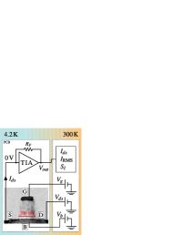
Measurements were carried out at , by dipping the samples in liquid \ce^4He, in order to observe electron localization and quantum transport in the device. We used a custom-made steel dip-stick provided of a 16-pin dual-in-line carrier and a custom cryogenic amplifierMazzeo et al. (2012); Tagliaferri et al. (2016a), described below, as a pre-amplification stage. Such cryogenic amplifier allowed to obtain simultaneous measurements of source-drain DC current and its rms noise level , or alternatively, coupled to a custom spectrum analyzerSampietro, Fasoli, and Ferrari (1999), the noise power spectral density at constant applied voltages (Figure 1a). Other relevant quantities like the differential conductance and transconductance are calculated from the DC measurements.
The key element of our measurement setup is a custom CMOS amplifier designed to operate at , which reduces the thermal noise of the resistors and transistors. In addition, the length of the connections between the cryogenic device and the first amplification stage is reduced from meters of a standard room temperature solution to the scale of the centimeter, thus cutting most of the parasitic capacitance and correspondingly the high frequency noise on current measurements, with respect to room-temperature amplification. The amplifier uses a transimpedance architecture with a resistive feedback that sets the current-to-voltage conversion factor. The feedback resistor is chosen as a trade-off between the input-referred current noise and the signal bandwidth, both inversely proportional to the resistor value. For better consistency, all the measurements reported in this work are taken with a feedback resistor of at 4.2 K that provides a bandwidth of and a noise level below to . The cryogenic amplifier has been implemented in a standard CMOS technology previously characterized at Guagliardo and Ferrari (2013), it occupies and has a static current consumption of with a power supply of .
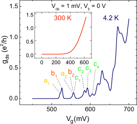
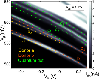
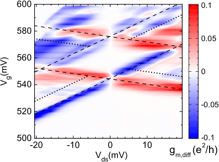
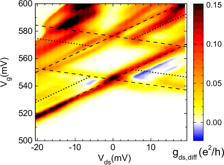
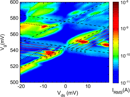
Conductance peaks in Fig. 1b show the resonant tunneling and Coulomb blockade behaviour in the device. The bulk potential is used as a back-gate to tune the electrostatic coupling between the localized states in the channel and the source/drain contacts, which behave as reservoirs with continuous energy spectrum up to their chemical potential Lansbergen et al. (2008); Prati et al. (2011); Prati and Shinada (2013); Prati et al. (2016). The vs stability diagram at a constant bias of mV is reported in Fig. 1c. As distinct confinement centers are coupled to the bulk gate differently depending on their position, the resonant tunneling levels result grouped as parallel lines of different slope associated to distinct electrostatic quantum dots and donors centred in the channel. The 2D stability diagrams in Fig. 2 of current, differential conductance and differential transconductance versus and give a broader view of the spectroscopy of the states in the device and are complemented by an rms stability diagram.
The association of the first electron levels of the device to two group V donor atoms is justified by three experimental facts. First, it is the presence of the two pairs of parallel lines (a1, a2 and b1, b2 respectively) in Fig. 1c with similar charging energy, with no further states at higher energy. It corresponds to the fact that a group V donor can bound only two electrons, forming a neutral () and a negatively charged () statesPrati and Shinada (2013). Second, the charging energy of both is about 19 meV which is in the range of around 15-20 meV reported in several worksTan et al. (2010); Prati et al. (2011); Pierre et al. (2010), Finally, conduction band transport occurs starting from 40-50 meV above such energy levels, which corresponds to the meV ionization energy of the ground state referred to the conduction band, which falls around 610 mV at 4.2K as from Fig. 1b. We thus reasonably conclude that, as expected by the fact that the channel is only 100 nm long and the annealing process operated during the fabrication, there are two donors participating to the transport in the channel, both by and states. The values of the charging and ionization energies along with the arsenic implantation for the ohmic contacts definition, suggest the single donors to be As atoms. At higher energy with respect to the donor states, the family of peaks referred to as c have a different slope and energy spacing than the donors, allowing occupation greater than two, which we attribute to a quantum dot electrostatically defined by some interface disorder which is not screened at cryogenic temperature and ultra-diluted electron density. Such observations are confirmed by the rigid translation of the stability diagram fingerprint given by the first and the second peaks in Fig. 2 that we observed by changing the bulk voltage. An interesting peculiarity of this device consists of its high conductance in units of which suggests a strong coupling regime of the donor states with the contacts.
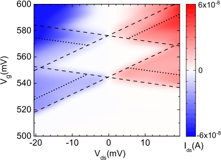
We now turn to the investigation of the electron transport in the device as carried out by first analyzing the Coulomb blockade diamond structures that best fit the data plotted in Fig. 2 according to the constant interaction model Kouwenhoven, Austing, and Tarucha (2001). Such measurements were all taken during the same thermal cycle, different than those of Fig. 1c: a small shift of the resonant tunneling features is observed between different thermal cycles, generally attributed to a different configuration of frozen surrounding charges in distant interface defects, but the relative positions of the peaks and the geometry of the Coulomb diamonds remains the same. Figure 2d) shows the RMS of the drain current as a function of the gate and drain voltages. For each measurement point the acquisition time was of enabling the calculation of the RMS value of the current noise on the full bandwidth of the amplifier starting from . The use of the cryogenic amplifier enhanced the RMS stability diagram measurements, as more resonant tunneling features were observed than in similar diagrams obtained with room-temperature amplification (see Supplementary Material). Closely spaced equidistant parallel lines terminating on the lines of the first electron state are detected (red lines in Fig. 2d): such features can not be attributed neither to density-of-state fluctuations in the contacts nor to excited states of the donor because they are symmetric and cross in points of zero bias towards lowest gate voltages respectively. Interestingly, their identical periodic spacing for both positive and negative bias voltage points towards tunneling events assisted by phonon emission on the two sides, as from Ref. 2. Such transport regime is further investigated in the following by looking at the noise spectrum.
The width and height of the main Coulomb diamond in Fig. 2, along with the slopes of its edges and of the red lines in Fig. 1c, are used to extract information about the donor states and the coupling with the transistor electrodes. From the width (i.e. the voltage distance of the corners with respect to the zero bias vertical line) the charging energy is estimated as .
The lever-arm factor is estimated to be . This value allows to calculate the total capacitance and the other values as follows:
Despite the uncertainty in these values due to graphical extrapolation, comparison between them provides insight on the location of the donor atom(s): since , the donor is similarly coupled to the source and drain contacts and therefore located near the center of the channel, as most probable from theory in order to observe some current flow.
The phonon energy spacing , again converted from the spacing between the corresponding red lines using the same lever-arm factor is around . Assuming the phonon velocity in silicon of about , the estimation of the corresponding wavelength is of the order of . In the hypothesis of an open phonon cavity originating these electron transport resonances, as from Ref. 3, the length of such a cavity corresponds to ; the resulting length of 2.6 nm is compatible with the longitudinal Bohr orbit diameter of As atoms in silicon which is 2.36 nm Prati and Shinada (2013); Van Donkelaar et al. (2015).
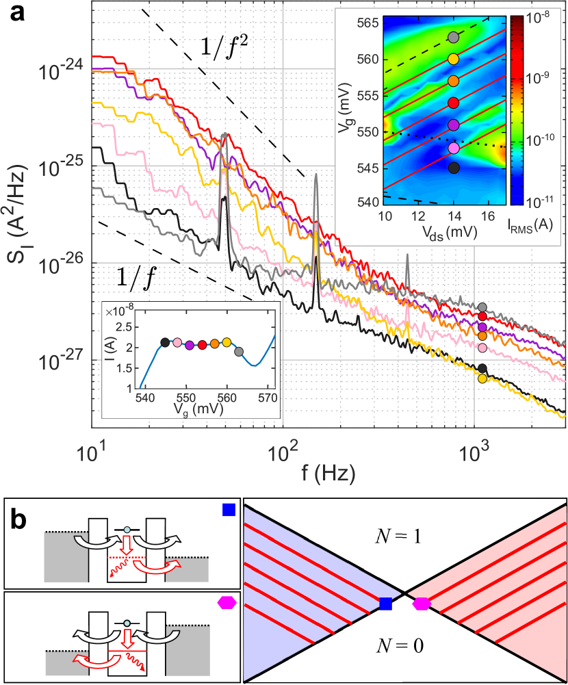
Additional information on the phonon-mediated tunneling process has been obtained by measuring the power spectral density of the source-drain current noise. For these measurements the device was tuned to a constant bias mV and to different values of in a range where the evenly-spaced lines associated to phonon-mediated tunneling occurs. Fig. 3(a) shows the comparison of the noise spectrum in regions where: current regularly flows through a state at energy far from the transition to the blocked regime, which results as typical noise (black dot), at the edge of the stability diagram where noise is observed at low frequency (gray), and in the regions where phonon emission occurs (yellow, orange, red, purple and pink dots). In this latter case a trend is observed according whether the respective lines are visible in the RMS stability diagrams at that bias voltage . Such low frequency noise can not be associated to the Lorentzian noise of a single defect as the characteristic frequency of the Lorentzian curve fitting the spectra is constant (around 12 Hz) in the whole range of the parallel features, differently than a charge Random Telegraph Signal (RTS). Furthermore, at such low temperature RTS of a single defect arises in energy intervals of few meV only. The spectra of Figure 3a corresponding to phonon lines are fitted by noise with two Lorentzian noise phenomena at 12 Hz and 2800 Hz respectively, both irrespective from the gate voltage. As they are observed only in correspondence of visible phonon emission lines, we attribute them to the decay of high frequency phonons to low frequency acoustic phonons during the cooling process of the crystal Galkina et al. (1987); Klitsner and Pohl (1987); Msall et al. (1993); Xie et al. (2013). The Fig. 3(b) shows the microscopic mechanism of phonon emission for the negative and positive current respectively. To summarize, the single phonon-mediated regime of the quantum transport occurs in such single electron filling of the single donor channel regime.
To conclude, we observe single phonon-mediated quantum transport by tracking the RMS noise in a nano-transistor operated in the single atom and single electron regime. The use of a cryogenic amplifier makes such measurement effective, by reducing the instrumental noise and the electromagnetic noise affecting the measurements when the amplification system is far from the device under test. The characterization of a commercial single electron transistor revealed the presence of a dopant in the channel, likely originated by unintentional diffusion from the source/drain contacts. The RMS measurements indicate the presence of few- down to single-phonon mediated tunneling, for which the low frequency spectrum results a Lorentzian typical of generation-recombination processes.
Data are available upon reasonable request.
References
- Fujisawa et al. (1998) T. Fujisawa, T. H. Oosterkamp, W. G. Van der Wiel, B. W. Broer, R. Aguado, S. Tarucha, and L. P. Kouwenhoven, Science 282, 932 (1998).
- Zwanenburg et al. (2009) F. A. Zwanenburg, C. E. van Rijmenam, Y. Fang, C. M. Lieber, and L. P. Kouwenhoven, Nano letters 9, 1071 (2009).
- Escott, Zwanenburg, and Morello (2010) C. C. Escott, F. A. Zwanenburg, and A. Morello, Nanotechnology 21, 274018 (2010).
- Granger et al. (2012) G. Granger, D. Taubert, C. Young, L. Gaudreau, A. Kam, S. Studenikin, P. Zawadzki, D. Harbusch, D. Schuh, W. Wegscheider, et al., Nature Physics 8, 522 (2012).
- Braakman et al. (2013) F. R. Braakman, P. Barthelemy, C. Reichl, W. Wegscheider, and L. M. Vandersypen, Applied Physics Letters 102, 112110 (2013).
- Braig and Flensberg (2003) S. Braig and K. Flensberg, Physical Review B 68, 205324 (2003).
- Crippa et al. (2019) A. Crippa, R. Ezzouch, A. Aprá, A. Amisse, R. Laviéville, L. Hutin, B. Bertrand, M. Vinet, M. Urdampilleta, T. Meunier, et al., Nature communications 10, 1 (2019).
- Turchetti et al. (2015) M. Turchetti, H. Homulle, F. Sebastiano, G. Ferrari, E. Charbon, and E. Prati, Applied Physics Express 9, 014001 (2015).
- Leti et al. (2011) G. Leti, E. Prati, M. Belli, G. Petretto, M. Fanciulli, M. Vinet, R. Wacquez, and M. Sanquer, Applied Physics Letters 99, 242102 (2011).
- Crippa et al. (2015) A. Crippa, M. L. Tagliaferri, D. Rotta, M. De Michielis, G. Mazzeo, M. Fanciulli, R. Wacquez, M. Vinet, and E. Prati, Physical Review B 92, 35424 (2015).
- Guagliardo and Ferrari (2013) F. Guagliardo and G. Ferrari, in Low-noise current measurements on quantum devices operating at cryogenic temperature, edited by E. Prati and T. Shinada (Pan Stanford Publishing, 2013) pp. 187–210.
- Tagliaferri et al. (2016a) M. L. V. Tagliaferri, A. Crippa, S. Cocco, M. De Michielis, M. Fanciulli, G. Ferrari, and E. Prati, IEEE Transactions on Instrumentation and Measurement 65, 1827 (2016a).
- Prati and Morello (2013) E. Prati and A. Morello, Single-Atom Nanoelectronics , 5 (2013).
- Vitusevich and Zadorozhnyi (2017) S. Vitusevich and I. Zadorozhnyi, Semiconductor Science and Technology 32, 043002 (2017).
- Mazzeo et al. (2012) G. Mazzeo, E. Prati, M. Belli, G. Leti, S. Cocco, M. Fanciulli, F. Guagliardo, and G. Ferrari, Applied Physics Letters 100, 213107 (2012).
- Tagliaferri et al. (2016b) M. L. V. Tagliaferri, A. Crippa, M. De Michielis, G. Mazzeo, M. Fanciulli, and E. Prati, Physics Letters A 380, 1205 (2016b).
- Sampietro, Fasoli, and Ferrari (1999) M. Sampietro, L. Fasoli, and G. Ferrari, Review of scientific instruments 70, 2520 (1999).
- Lansbergen et al. (2008) G. Lansbergen, R. Rahman, C. Wellard, I. Woo, J. Caro, N. Collaert, S. Biesemans, G. Klimeck, L. Hollenberg, and S. Rogge, Nature Physics 4, 656 (2008).
- Prati et al. (2011) E. Prati, M. Belli, S. Cocco, G. Petretto, and M. Fanciulli, Applied physics letters 98, 053109 (2011).
- Prati and Shinada (2013) E. Prati and T. Shinada, Single-atom nanoelectronics (Jenny Stanford Publishing, 2013) p. 16.
- Prati et al. (2016) E. Prati, K. Kumagai, M. Hori, and T. Shinada, Scientific reports 6, 19704 (2016).
- Tan et al. (2010) K. Y. Tan, K. W. Chan, M. Mottonen, A. Morello, C. Yang, J. v. Donkelaar, A. Alves, J.-M. Pirkkalainen, D. N. Jamieson, R. G. Clark, et al., Nano letters 10, 11 (2010).
- Pierre et al. (2010) M. Pierre, R. Wacquez, X. Jehl, M. Sanquer, M. Vinet, and O. Cueto, Nature nanotechnology 5, 133 (2010).
- Kouwenhoven, Austing, and Tarucha (2001) L. P. Kouwenhoven, D. Austing, and S. Tarucha, Reports on Progress in Physics 64, 701 (2001).
- Van Donkelaar et al. (2015) J. Van Donkelaar, C. Yang, A. Alves, J. McCallum, C. Hougaard, B. Johnson, F. Hudson, A. Dzurak, A. Morello, D. Spemann, et al., Journal of Physics: Condensed Matter 27, 154204 (2015).
- Galkina et al. (1987) T. I. Galkina, A. Y. Blinov, M. Bonch-Osmolovskii, O. Koblinger, K. Lassmann, and W. Eisenmenger, Physica Status Solidi B (1987).
- Klitsner and Pohl (1987) T. Klitsner and R. Pohl, Physical Review B 36, 6551 (1987).
- Msall et al. (1993) M. Msall, M. Carroll, J. Shield, and J. Wolfe, in Phonon Scattering in Condensed Matter VII (Springer, 1993) pp. 116–117.
- Xie et al. (2013) G. Xie, Y. Guo, B. Li, L. Yang, K. Zhang, M. Tang, and G. Zhang, Physical Chemistry Chemical Physics 15, 14647 (2013).