Band Bending and Valence Band Quantization at Line Defects in MoS2
Abstract
The variation of the electronic structure normal to 1D defects in quasi-freestanding MoS2, grown by molecular beam epitaxy, is investigated through high resolution scanning tunneling spectroscopy at K. Strong upwards bending of valence and conduction bands towards the line defects is found for the 4|4E mirror twin boundary and island edges, but not for the 4|4P mirror twin boundary. Quantized energy levels in the valence band are observed wherever upwards band bending takes place. Focusing on the common 4|4E mirror twin boundary, density functional theory calculations give an estimate of its charging, which agrees well with electrostatic modeling. We show that the line charge can also be assessed from the filling of the boundary-localized electronic band, whereby we provide a measurement of the theoretically predicted quantized polarization charge at MoS2 mirror twin boundaries. These calculations elucidate the origin of band bending and charging at these 1D defects in MoS2. The 4|4E mirror twin boundary not only impairs charge transport of electrons and holes due to band bending, but holes are additionally subject to a potential barrier, which is inferred from the independence of the quantized energy landscape on either side of the boundary.
keywords:
band bending, scanning tunnelling spectroscopy, MoS2, polarization charge, mirror twin boundaryUni Koeln] II. Physikalisches Institut, Universität zu Köln, Cologne D-50937, Germany \alsoaffiliation[Uni Muenster] Institut für Materialphysik, Westfälische Wilhelms-Universität Münster, Münster D-48149, Germany Uni Koeln] II. Physikalisches Institut, Universität zu Köln, Cologne D-50937, Germany THP] Institut für Theoretische Physik, Universität zu Köln, Cologne D-50937, Germany Dresden] Institute of Ion Beam Physics and Materials Research, Helmholtz-Zentrum Dresden-Rossendorf, Dresden D-01328, Germany \alsoaffiliation[Aalto] Department of Applied Physics, Aalto University School of Science, Aalto FI-00076, Finland Aalto] Department of Applied Physics, Aalto University School of Science, Aalto FI-00076, Finland \alsoaffiliation[Oulu] Microelectronics Research Unit, University of Oulu, Oulu FI-90014, Finland Uni Koeln] II. Physikalisches Institut, Universität zu Köln, Cologne D-50937, Germany
Coupled to the rise of MoS2 and other transition metal dichalcogenide (TMDC) semiconductors as prospective two-dimensional (2D) device materials came the need to investigate their one-dimensional (1D) defect structures, e.g. grain boundaries (GBs). Depending on their structure, GBs impair device performance to differing degrees when positioned in the channel of a single layer MoS2 field effect transistor 1, 2, 3, 4. It is thus evident that control of the type and concentration of GBs is of importance for device fabrication. Besides satisfying scientific curiosity, it therefore pays to understand their effect on band structure and charge carrier transport. The lowest energy GBs are those hardest to avoid during growth, as the energy penalty associated with their introduction is marginal. In the three-dimensional (3D) world, these low energy GBs are 2D stacking faults or twin planes. For the case of SiC devices such defects cause increased leakage current, reduced blocking voltage, and the degradation of bipolar devices 5, 6. In the world of 2D materials, the analog to twin planes is 1D mirror twin boundaries (MTBs). These structural defects have some surprising effects on the band structure of monolayer MoS2, to be investigated in this manuscript.
GBs in MoS2 layers have already been intensively investigated. Experimentally, scanning tunneling microscopy (STM) and spectroscopy (STS) are the ideal tools to identify and characterize MoS2 GBs electronically7, 8, 9, 10, 11. Despite large variations in magnitude, typically an upwards shift of the valence band (VB) and often also of the conduction band (CB) is observed at the GB 7, 12, 8, 10, 11, 9. The magnitude of the reported shifts range from 0.15 eV to 1.0 eV for the VB, depending on substrate and GB type. CB shifts may be of the same magnitude, but are usually smaller. The spatial extension of the band bending is on the order of nm away from the GB. Similar band bending effects were also described for MoS2 12, MoSe2 and WSe2 edges 13, 14, as well as for lateral heterojunctions, e.g. of MoS2 with WS2 or WSe2 15, 16. As an explanation for the observed band bending strain 7, 8, 17, 16, charge transfer into in-gap states 12, 4, 18, or a combination of both were invoked 10, 9, 15. Despite the technological importance of the band bending, modifications of the electronic structure around GBs are still poorly understood.
Here, for the investigation of 1D line defects in MoS2, we take an approach different from previous work. Molecular beam epitaxy (MBE)19, rather than the typical chemical vapor deposition, is employed for the growth of the MoS2 layer to be investigated by STM and STS. The advantage is that the MoS2 layer is grown under ultra-high vacuum conditions and remains thereunder for spectroscopic investigation. Thereby the MoS2 and the potentially reactive 1D defects remain clean of adsorbates. Inert, single-crystal graphene (Gr) on Ir(111) is used as a substrate 20. Consequently, high-resolution STS is facilitated and ambiguities in the comparison of the data to density functional theory (DFT) calculation, which could result from adsorption or an inhomogeneous environment, are avoided. We discover that band bending over a distance of nm and the associated confinement normal to the 1D line defect renders the MoS2 VB quantized. Although we focus our investigation on the most frequent and presumably lowest energy MTBs 21, 22, we find the same phenomenon for the edges of monolayer (ML) and bilayer (BL) MoS2 islands, as well as for less symmetric, higher energy GBs. From the comparison between the experimental and calculated results, we establish that the band bending is not caused by strain but by charge on the line defects. Using DFT and measuring the Fermi wave vectors of MTB states, we decompose the net charge on the line defects into contributions from polarization and in-gap states of the 1D line defects. Charge transfer from Gr into in-gap defect bands is of decisive importance for band bending and the formation of the hole confining potential in the VB, meaning that this effect is substrate-tunable.
1 Results and Discussion
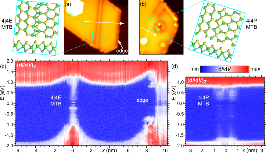
Scanning Tunneling Spectroscopy. The STM topographs in Figures 1a and 1b show the 1D defects typical for MBE-grown ML-MoS2 islands, in our case on Gr/Ir(111) (see Methods). A 4|4E- and a 4|4P-type MTB are visible in Figures 1a and 1b, respectively; their atomic structures are depicted, illustrating that they form between -misoriented domains. 4|4E- or 4|4P-type MTBs appear in topographs as bright single- or double-tracks, respectively (see Ref. 22 for details). The MTBs host 1D metallic states and consist of 4-fold rings sharing an edge along a Mo-S bond (hence named 4|4E) or sharing a point at S-dimer sites (hence named 4|4P) 23, 24, 25, 22. In MoSe2 and MoTe2 the 4|4P-type MTB is energetically most favorable, while in MoS2 both 4|4P- and 4|4E-types are stable 21, 26. In our samples, 4|4E-type MTBs are about times more common and typically longer than 4|4P-type. An atomically straight zigzag island edge, parallel to the MTB, is also indicated in Figure 1a.
We perform high-resolution, constant height STS linescans orthogonally across the 1D defects; in Figure 1c over the 4|4E MTB and continuing over the island edge, in Figure 1d over the 4|4P MTB. The meV-, Å-resolution of the linescans leaves no data interpolation or filtering necessary (see Methods). In the colorplot, blue represents a low or zero signal intensity (i.e. in the band gap) while the red end of the scale signifies a finite density of states. The unperturbed or ‘bulk’ ML-MoS2 band structure is measured when sufficiently far from defects, for example in Figure 1c at nm: at eV the onset of the CB and at eV that of the VB are seen by STS.27
Scanning orthogonally over the 4|4E MTB, defined to lie at nm in Figure 1c, both the VB and CB bend several hundred meV upwards (i.e. towards higher energies). This bending occurs in a range of nm on both sides of the MTB. No band bending of significance could be detected beyond this range 28.States are detected throughout the band gap at the location of the MTB. They are derived from the 1D metallic MTB bands in the band gap of the 2D MoS2 22. Their quantization and Coulomb-blockade energy gap, associated with the Tomonaga-Luttinger liquid hosted along the finite-length MTB,22 are visible close to . Towards the island edge (located at nm) similar upwards bending and in-gap states are observed. Finally, the relatively featureless spectra of Gr on Ir(111) are recorded for nm. In Figure 1d the 4|4P-type MTB is located at nm. The double-track structure of the 1D metallic states 22 is faintly visible. In contrast to the 4|4E MTBs and edges, the 4|4P MTB does not cause significant band bending. Further measurements confirming this are available in the Supporting Information, Figure S1.
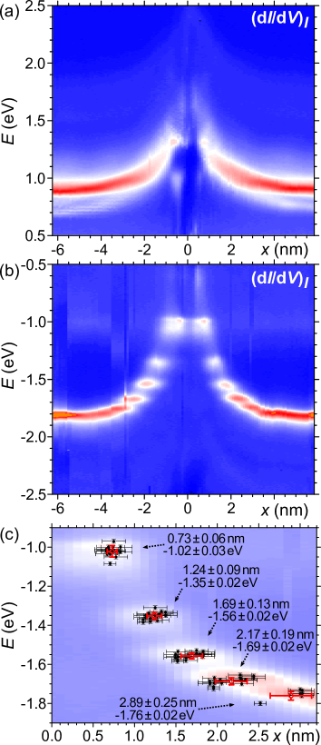
We focus on the large band bending seen at 4|4E MTBs, and obtain additional information via constant current STS; exemplary linescans are shown in Figures 2a and 2b. Constant current STS is of higher sensitivity to the variations at the band edges, i.e. to abrupt increases of the LDOS due to van Hove singularities, and thus can better resolve the subtle features at the edges, while features within the bands are hardly visible.29, 30. We note that similar band edge resolution with an inferior signal-to-noise ratio can be achieved by constant height STS after normalizing to the tunneling current (compare Figure S2).
The 1D MTB band is metallic and was visible at in the constant height STS of Figure 1c. However, with increasing magnitude of bias voltage no abrupt increase of the LDOS takes place in the investigated ranges of Figure 2(a,b), and so the 1D MTB band is not visible in constant current STS. Well-visible in the constant current STS are the conduction and the valence band edges in Figure 2a and Figure 2b, respectively, through a sudden intensity rise.
In the CB, Figure 2a, far from the MTB we see the Q-point edge states at eV and, faintly, the K-point edge states at eV 27. The latter is the CB minimum of ML-MoS2 and is barely visible in constant height STS due to its large parallel momentum, but constant current STS allows the tip to move closer to the sample to detect this weak signal 27, 29. Towards the MTB, the bands are bent smoothly up to roughly eV. The K-point edge appears to bend slightly more than the Q-point edge, until their signals merge around nm from the MTB. Bending of higher energy band edges is also faintly visible.
In the VB, Figure 2b, the dominating -point edge begins at around eV and bends upwards to eV at the MTB, thus undergoing larger bending than the CB. The VB bending occurs stepwise in increasing energy intervals. The discrete energies are near identical on either side of the MTB and were approximately the same across dozens of such MTBs of various lengths, see Figure 2c.
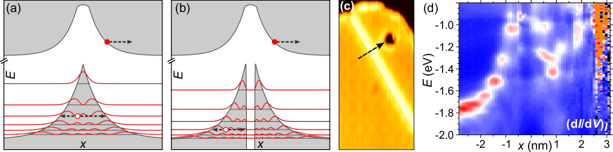
We consider a simple explanation for these discrete energies: the bending of the VB creates a potential well as sketched in Figure 3a. This confinement quantizes the VB energy levels perpendicular to the MTB, whereas electrons excited to the CB are not confined. The energy levels and the maxima of the squared wave functions at the edge of the potential are reasonably well reproduced by solving the 1D Schrödinger equation for holes in the shown potential. The strongest probability density maxima of the quantized states are located close to the bent VB edge, with additional small peaks closer to the MTB. These smaller peaks are invisible to constant current STS (compare Figure 2b), while constant height STS shows featureless intensity below the band edge next to the MTB (compare Figure 1c). To understand this, it is important to note that the states represented in Figure 3a are 1D solutions of the Schrödinger equation for a 1D potential normal to the MTB. In reality they mark the van Hove singularities of confined states that disperse parallel to the MTB. Their hole dispersion along the MTB is characterized by downwards, open parabolas which overlap throughout below the band edge, but not at the band edge. Thus the edge-sensitive constant current STS mode measures only the dominant van Hove singularities, while constant height STS measures a featureless LDOS below the bent VB edge due to overlapping states.
An alternative scenario to the single potential well consists of two independent wells, left and right of the MTB, with the MTB acting as a repulsive barrier. It allows one to recreate the observed peaks as well, as suggested by Figure 3b. We note that distinction of these two situations is relevant, as hole transport through the MTB will be strongly impaired if the MTB acts as a repulsive potential for holes.
Experimentally it is straightforward to distinguish these two situations. Figure 3c shows a MoS2 island which features a small vacancy island directly next to a 4|4E MTB. An STS linescan from the complete side of the MTB to the broken side is displayed in Figure 3d. On the complete side the quantized energy levels of the VB are like that at a ‘pristine’ MTB, compare Figure 2c. On the other side, however, the quantized states are strongly modified due to the changed potential energy landscape. The eigenenergies and eigenstates on the complete side are not perturbed by the environment on the broken side, making plain that the two sides are independent — the MTB is a barrier to holes confirming the scenario of Figure 3b.
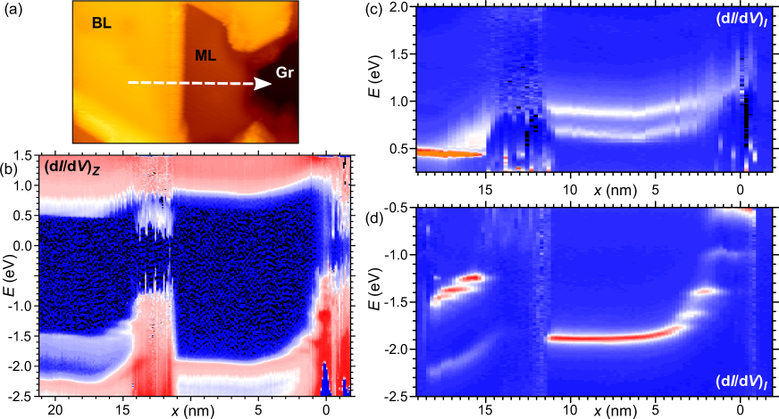
Does the VB bending at a MoS2 island edge, as visible in Figure 1c, cause quantization similar to that at a MTB? And does such band bending also occur at BL-MoS2 island edges? To answer these questions we perform STS linescans along the path marked in Figure 4a, from a BL-island via BL- and ML-MoS2 edges down to the Gr level. In constant height STS, Figure 4b, it is seen that also the BL-MoS2 bands undergo upwards bending at the island edge, similar to in the ML. Both of the BL’s split -point bands (at eV and eV at nm) are bent upwards at the edge. More information is gathered from constant current STS of the CB and VB energy ranges shown in Figures 4c and 4d, respectively. The BL CB edge appears to bend eV upwards, while in the ML bending of the K- and Q-point states (with slightly different curvatures) bears a resemblance to that at 4|4E MTBs (Figure 2a) and is of the order of 0.5 eV. Although STS at MoS2 edges is typically affected by tip instabilities like those visible in Figure 4d, quantization of the VB is unambiguous next to both the BL- and ML-MoS2 island edges. While the discrete VB energy values were approximately the same for other ML island edges, the characteristic energies differ from those observed at 4|4E MTBs (Figure 2b,c). We have additionally observed VB quantization at some tilt GBs, see Figure S3.
Density Functional Theory Calculations. Band bending may be caused by charge accumulation or depletion, but charge density is not directly probeable by STM/STS, typically. To uncover the mechanism of charging, we compare our experimental results to DFT calculations. Figure 5a shows the geometry of a ML-MoS2 ribbon containing a 4|4E-type MTB, the Gr substrate, and the size of the two DFT supercells used to calculate the freestanding MoS2 ribbon and the MoS2 ribbon on Gr (see Methods).
We first focus on the freestanding ribbon with a 4|4E MTB. In Figure 5b, the S-atom core potential variation perpendicular to the 4|4E MTB is plotted (red crosses). The 4|4E MTB is at a higher potential than the ribbon edges, and they are connected through a near-linear slope. In Figure 5c the corresponding projected LDOS is displayed. We focus on S atoms because they contribute most to the STS signal, being closest to the STM tip. Via STS simulations for pristine MoS2, we verified the S atoms’ dominant contribution and note that the LDOS for Mo atoms displays qualitatively the same features. The variation in the band edge positions in Figure 5c reflects that of the core potentials. The near-linear potential gradient can be reproduced by describing the MoS2 ribbon as a sheet of thickness and effective dielectric constant (compare Ref. 31) containing three parallel wires of line charge , corresponding to the MTB and the two edges. See Figure S4 for details. Through comparison with our DFT we estimate at the MTB and at each edge. Here is the elementary charge and Å the primitive translation of MoS2 along the line.
The net line charge is composed of two contributions: (i) the 1D MTB band carries a charge defined by the Fermi wavevector . The band structure of a freestanding ribbon is shown in Figure 5d, with MTB and edge bands found inside the bulk gap. Corresponding in-gap states are visible at the MTB and edges in Figure 5c. For the MTB band is located at and, since the band is hole-like, its filling is . Therefore the MTB band carries a band charge (cf. for a full band). (ii) Evidently, there must be an additional positive charge contribution to the MTB in order to reach the much smaller net line charge of . The ribbon is composed of two MoS2 domains of opposite orientation and opposite formal polarization .32, 33 At the MTB, the abrupt change in polarization induces a polarization charge (discussed in more detail below). As we deduce on the MTB. The nearly complete compensation of band and polarization charge can be rationalized as follows: the electrostatic energy created by the polarization of the MoS2 drives the filling of the 1D MTB and edge bands in order to minimize system energy.33 In fact, in the limit of infinite ribbon width is exactly zero, as otherwise the energy of the electrostatic field would diverge (‘the polar catastrophe’).33
When the MoS2 ribbon is placed on Gr, a total charge of is depleted from the Gr layer and added to the MoS2 ribbon, as determined from Bader charges34 and illustrated by the charge density difference in the side view of Figure 5a. Most of this charge is located at the MTB and ribbon edges, with less in the ‘bulk’ regions between. Dividing the MoS2 ribbon into MTB and edge regions, we estimate an excess of located at the MTB and at each edge. Considering the breadth of the supercell, this equates to linear charge densities of and at MTB and edge, respectively. These transfer charge densities should be added to those of the freestanding MoS2 ribbon, i.e. a total of / is predicted at the 4|4E MTB in MoS2 on Gr. Note that, unlike in the MoS2 ribbon, the charge distribution in Gr is relatively uniform (compare Figures 5a and S5) indicating a rather large screening length in Gr.
The origin of charge transfer from Gr to the MoS2 is the work function difference between Gr and ML-MoS2. According to DFT and in agreement with experiment, the work function of Gr is lower than the work function of MoS2. DFT (experimental) values are around eV ( eV) for Gr and eV ( eV) for ML-MoS2.35, 36, 37, 38 Consequently, when MoS2 is placed on Gr, the Fermi levels will align through charge transfer. The charge transfer will thus decrease the chemical potential in Gr, and increase the chemical potential in MoS2. If our model for determining is valid, one should also be able to extract the charge transfer from the change in filling of the MTB band. The band structure from the MoS2/Gr supercell is shown in Figure 5e. Note that due to the incommensurate unit cells of MoS2 and Gr the supercell construction must be used, resulting in band folding. This is then displayed in the periodic zone scheme with the MTB band highlighted. We extract the Fermi wavevector of the 1D MTB band (where denotes the presence of Gr). This corresponds to the filling of the hole-like band being increased from to , i.e. the 1D band charge is increased by , in decent agreement with our Bader charge transfer analysis above (). In experiment, we measure standing waves along the 4|4E MTB of periodicity corresponding to a Fermi wavevector (see Ref. 22), in agreement with the DFT value . Our conclusions here are in line with Kaneko et al. 18, who speculated that the accumulation of charge transferred from the substrate into 1D MTB bands could be the origin of a substantial band bending at MoS2 MTBs.
Figure 5f shows the projected LDOS of the S atoms perpendicular to the 4|4E MTB for the ribbon on Gr. Large upwards band bending occurs at the MTB and edges in the CBs and VBs, in qualitative agreement with experiment and consistent with the negative line charges on them. Due to the limited cell size the band bending is smaller in magnitude than in experiment; the MoS2 band structure does not reach its ‘bulk’ state between the MTB and the edges (compare to the case of an asymmetrically positioned MTB in Figure S6). The S-atom core potentials for the ribbon with a 4|4E MTB on Gr are plotted in Figure 5b as blue crosses. They reproduce the variation of the band edge energy with the spatial coordinate.
Corresponding results for the 4|4P-type MTB are shown in Figure 6. The S-atom core potentials for the freestanding ribbon, shown in Figure 6a, indicate that the MTB is positively charged. The ribbon on Gr, on the other hand, shows hardly any band bending in the core potentials or in the projected LDOS (Figure 6b), as also observed in experiment. Again, charge transfer from Gr to MoS2 takes place when the layers are brought into contact (compare band structures Figure 6c,d), but results in a nearly neutral net line charge. This implies that polarization charge and 1D band charge compensate fully (), and indeed this conforms with our understanding of the system. Assuming the same polarization charge as for the 4|4E MTB would result in an estimate of . For the electron-like 1D MTB band () this corresponds to a Fermi wavevector of . This is in excellent agreement with our calculated DFT value (Figure 6d) and our experimental measurement of [based on standing wave periodicity in 4|4P MTBs, see Ref. 22].
Rephrased, because the charge transfer from Gr fortuitously results in for our 4|4P MTB, the measurement of the Fermi wavevector of the 1D MTB band implies a measurement of the polarization charge . To the authors best knowledge, this is the first direct measurement of a polarization charge. The measured value exactly matches predicted by Gibertini and Marzari33 for 4|4P MTBs. More strictly, we are referring here to the ‘bound charge’ which is the sum of and a correction for the changed stochiometry of the interface. The 4|4E MTB was not calculated in Ref. 33, but – considering the MoS2 lattice symmetry and the boundaries’ shared Mo2S2 stochiometry – the 4|4E MTB must possess the same quantized bound and polarization charge as its 4|4P counterpart.
We note that placing MoS2 on Gr as charge reservoir already captures the essence of the processes; the Ir(111) substrate, omitted due to computational limitations, does not change the picture qualitatively. We attribute this to the circumstance that Gr on Ir(111) is almost undoped (Dirac point only 0.1 eV above ); its work function is nearly identical to that of freestanding Gr. However, since Gr offers poor lateral screening, the Ir substrate will affect the lateral screening substantially.
ey 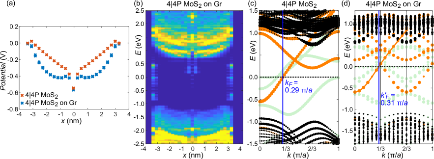
In our DFT calculations we see no significant lattice strain (%) in the bulk due to MTBs or island edges, ruling out its relevance for band bending. This is consistent with DFT calculations showing that MTBs induce strain only within nm normal to their axis 39, 40, i.e. on a length scale ten times smaller than that of our bending. In previous works TMDC band bending was ascribed to strain at the 1D interfaces 16, 17, 8, 40, or a combination of charging and strain 7, 15, 10, 9. This may be meaningful for low-symmetry tilt GBs composed of arrays of point dislocations giving rise to large local strains7, or lateral heterostructures with mismatch strain16, but not for the present case of perfect 4|4E MTBs and straight edges.
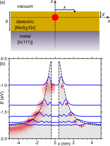
Continuum Modeling. The potential used in Figure 3b to reproduce the quantization at the 4|4E MTB was fitted ‘by hand’ and not based on a physical origin. In the following we will use the 4|4E MTB linear charge density as derived from DFT and physically meaningful system parameters in a simplistic model, in an effort to reproduce the band bending potential and the resultant dominant probability density maxima in and , as visible in experiment.
The band bending in the MoS2 ribbon on Gr/Ir(111) is modeled by a screened electrostatic potential due to an infinite line of charge located at the MTB, sandwiched between vacuum and a perfect metal substrate, as sketched in Figure 7a. Following the work of Le Quang et al. 14, the MTB charge ‘generates’ image charges in the vacuum and the metal, which themselves generate additional image charges, and so on to the th order. The potential at the MoS2 surface at a lateral distance is then:
| (1) |
where , , and are the dielectric constants of the dielectric layer and vacuum respectively, is the linear charge density at the MTB, and are as defined in Figure 7a, and is a potential energy offset (as any potential energy is only defined relative to another). The first term in Eq. (1) corresponds to self-screening by the dielectric only, while the second term in Eq. (1), the summation of potentials due to image charges to the th order, is due to metal screening. Finally, at the location of the MTB we add a potential barrier of depth eV and width nm by hand. We solve the Schrödinger equation for positive charge carriers of effective mass in the resultant potential.
As it is the -point which is detected in STS in the VB, we use an effective hole mass 41, 42. We consider the charge to be located in the center of the ML-MoS2 layer, thus nm. For simplicity, we model the MoS2 and Gr (and their van der Waals gaps) together as a single dielectric layer of thickness nm. Gr is only slightly doped in this configuration 43, 44, and thus expected to screen rather weakly, consistent with the nearly uniform charge distribution in Gr in Figure 5a. Indeed, considering Gr to be part of the perfect metal substrate leads to an over-estimation of the screening 14. The dielectric constant of ML-MoS2 is anisotropic and non-trivial 31, 45, and is complicated further by combination with Gr in our model. It is typically in the range , with similar values predicted for a ML-MoS2/Gr heterostructure.46
Setting , and with only and as variables, we find that values of and eV yield a very good fit, Figure 7b. The potential reproduces the lateral positions of the main probability density maxima and the energy level positions with error less of than eV, see Table S1 in Supporting Information.
This continuum modeling neglects the atomistic details of the system, the anisotropy of its screening, and simplifies its layered structure. Nevertheless, it captures the system’s essentials. Using literature-based estimates for , , , and the linear charge density obtained by DFT, the modeling reproduces eigenenergies and spatial positions of the quantized VB states at 4|4E MTBs.
Discussion. Based on literature reports, band bending of the VB and the CB at 1D defects appears to be the rule rather than the exception in TMDC semiconductors 12, 7, 8, 10, 11, 9, 13, 14, 15, 16. Our results are in line with this general finding, although the 4|4P MTB does not show band bending. Specifically, at 4|4E MTBs both charge carrier types face a significant potential barrier, with obvious negative implications for the conductivity of the MoS2. Electrons face a barrier of at least eV, while holes become trapped in an even deeper potential well.
A key point emerging from our DFT calculations is that the band bending depends heavily on the substrate, as the substrate’s electronic properties – specifically its work function – determine the amount of charge transferred. For our case of slightly p-doped Gr (Dirac point eV above 44), electron transfer from the substrate to the 1D defects prevails, causing an upward shift of the bands next to 4|4E MTBs and layer edges. By strong n- or p-doping of Gr, its work function 47, 48, thus the charge transfer, and consequently the amount of band bending at each 1D line defect is likely to be changed. This could for instance cause upwards or downwards bending also at the 4|4P MTB, for which we consider the absence of band bending in our measurements to be coincidental and related to the specific amount of charge transferred to the system. The sensitive dependence of the band bending on the environment could also partly explain why the measured band bending for MoS2 GBs with similar tilt angles differs vastly 7, 4, 9, 11.
If the nature of the substrate or chemical gating are able to affect band bending, electrostatic gating will do so as well. Thus the magnitude of band bending at a 1D defect is not a fixed quantity, but will change during device operation. On one hand, this will make the effect of 1D defects on charge carrier transport harder to predict. On the other, it could mean that the transport through MTBs and the carrier trapping at MTBs/edges can be controlled or switched via gating.
For hole transport through 4|4E MTBs, perhaps an even greater hurdle than bent bands is the repulsive barrier, which is obvious from the complete independence of the quantized VB states on either side of the MTB. Though tunneling transport is likely to take place (in our modeling the barrier width was set to nm), the transmission will be strongly diminished by the barrier. The barrier is a natural consequence of the broken crystal symmetry at the location of the MTB, causing back-scattering. Though speculation, it is likely that similar barriers for holes exist also for other grain boundaries, e.g. at the 4|4P MTB. It thus seems that hole transmission across MTBs is not only suppressed in the energy range of the spin-orbit splitting of the VB due to spin-valley locking, as described by Pulkin and Yazyev 49, but is globally impaired due to a barrier at the location of the MTB causing backscattering. Indeed Park et al.50 have noted a strong suppression of transmission deep within the VB at 4|4P MTBs. Considering these results, it appears rewarding to investigate hole transport across 4|4E and 4|4P MTBs in more detail, for example with a 4-probe STM.
In our work, quantization in the VB next to line defects was found whenever a substantial upwards shift of several hundred meV was observed: at 4|4E MTBs, at ML and BL edges, as well as at low symmetry GBs (see Supporting Information). It is evident that such quantization effects should also be present in other, similar systems which display band bending. Consequently the question arises: why has such quantization not been noted in the past? Firstly, we remark that the constant height STS linescan of a BL-MoSe2 edge by Zhang et al. 13 (compare Figure 3b of Ref. 13) indeed displays step-like features in the upper VB edge, which could be interpreted as signatures of VB quantization in view of the current findings. Next, we note that the VB states were made clearly visible only by constant current STS (or equivalently normalized constant height STS, see Figure S2), conducted with sufficient resolution and at low temperature.
Based on our DFT calculations we obtain the net line charge on the 4|4E MTB in MoS2 on Gr. Due to the marginal doping of Gr on Ir(111), this is also expected to be a reasonable estimate for that on Gr/Ir(111). Using this line charge and realistic system parameters, we were able to fit energy and location of the confined states in the VB accurately with a simple electrostatic model 14. Though imperfect, the agreement is reasonable and substantiates a net line charge of . Our result is similar to those obtained by Le Quang et al.14, with for the edge of a trilayer WSe2 flake, while Kobayashi et al.15 obtain linear charge densities an order of magnitude larger for a MoS2-WS2 1D heterojunction interface.
The 2D interfaces of insulating oxide heterostructures can be electrically conductive, in contrast to their bulk constituents. The origin of this conductivity is a matter of debate; a proposed mechanism is the formation of polarization charge at the interface to avoid a so-called ‘polar-catastrophe’.51 The study of analogous polar discontinuities at the 1D interfaces of 2D materials is an emerging field 52, 53, 54. To the best of our knowledge, the quantitative verification of the polarization charge at the MTBs here represents the first experimental measurement of such interface polarization charge. Considering the complications due to defects and intermixing at 3D hetero-interfaces,55, 56 the pristine interfaces of MoS2 MTBs may act as a reduced-dimensionality testing ground for polar-charging models.
The well-defined band bending and localization of charges at 4|4E MTBs and edges could find application in optics and optoelectronics. The asymmetry of the bending means a decreasing exciton energy profile towards the defect, possibly leading to an exciton funneling effect as has been achieved through strain-induced bending 57, 58 – it might also be possible to control the funneling via the aforementioned electrostatic gating. In analogy to TMDC semiconductor point defects having bound excitons 59, 60 and serving as single photon emitters 61, the quantized VB states next to 1D defects in MoS2 could also be utilized.
2 Conclusions
In summary, we have investigated the electronic landscape perpendicular to line defects in MoS2 islands with high-resolution STS. Band bending occurs in a nm range at MTBs and ML- as well as BL-island edges, as a result of charge on these 1D defects. Our experiments and DFT calculations develop a fully consistent picture of the defect charging, which is in agreement with literature predictions. 18, 33 Namely, the net line charge on MTBs in MoS2 is the result of polarization charge, its compensation by 1D MTB band-filling, and additional charge transfer into these in-gap bands due to the substrate’s different work function. Our work shows that STS is a viable tool to investigate the charging of domain boundaries. For the 4|4P MTB the absence of band bending implies the net absence of charge on the MTB. Therefore, via the STS measurement of the 1D band charge on the MTB, a first direct confirmation of the quantized polarization charge on MTBs was possible, precisely confirming the value of predicted by Gibertini and Marzari33. For the 4|4E MTB, the knowledge of the quantized polarization charge together with the measurement of the 1D band charge allows us to estimate the net charge on the MTB, which is in excellent agreement with the prediction of the DFT calculation.
The large ( eV) VB bending normal to the 4|4E-type MTBs on Gr/Ir(111) leads to VB quantization next to it, with a barrier at the MTB creating two independent confining potentials for holes to its left and right. Therefore, hole transport through these MTBs is suppressed. Using a simplistic electrostatic model, with realistic system parameters and the DFT-derived line charge , the resulting screened potential reproduces band bending accurately. Solving the 1D Schrödinger equation for this potential reproduces the eigenenergies and spatial position of the dominant peaks in the probability density. The CB next to 4|4E MTBs displays band bending too, thus CB electron transport is also substantially impaired. Hence this MTB is a considerable barrier to both charge-carrier types. Based on our findings, band bending of the VB and CB normal to the 1D line defects is proposed to be tunable through chemical or electrostatic gating.
3 Methods
Samples were grown in situ in a preparation chamber with a base pressure mbar connected to a K bath cryostat STM system. Ir(111) was cleaned by cycles of keV Ar+ ion erosion and flash annealing to K. Gr is grown on top by room temperature ethylene exposure till saturation and subsequent thermal decomposition at K. The resulting well-oriented Gr islands are grown to a complete single crystal Gr layer through exposure to L ethylene at K 62. MoS2 is grown at K on Gr/Ir(111) by Mo deposition with a flux of about atoms m-2 s-1 in a background elemental sulfur pressure of about mbar. Subsequently the sample is annealed for s at K in a S pressure of the same magnitude. Compare Ref. 19.
STM and STS measurements are performed at K and pressures mbar. STS is carried out with the lock-in technique, using a modulation frequency Hz and modulation voltage mV. This yields an experimental resolution of meV or better 63. We use both constant height [recording ] and constant current [] STS, where is the tunneling current, the bias voltage, and the height of the tip above the sample. In both modes is recorded while is ramped. For further explanation see Ref. 27. A linescan consists of a sequence of spectra taken at most Å apart along a straight line. In each spectrum, data points are taken every meV depending on the desired resolution. The path of the linescan may not be perfectly normal to the 1D defect, but the resulting error in can be neglected — in the scan of Figure 1c, for example, this amounts to a factor cos. The color plots of the linescans show raw data; no interpolation or smoothing is involved.
All density functional theory calculations were carried out using Vienna Ab Initio Simulation Package (VASP) 64, 65. The plane wave cutoff was set to 400 eV throughout. The atomic structure for the ML-MoS2 ribbon with MTB and unpassivated Mo-edges on Gr, as shown in Fig. 5, was constructed as follows. While the strain in the direction perpendicular to the MTB () is naturally released in the ribbon geometry, a suitable supercell needs to be constructed to release strain in the direction parallel to the MTB (). Since of MoS2 fairly closely matches with of Gr, we use a MoS2 layer consisting of 3(12+12) unit cells (12 units in each side of the MTB) and a Gr layer consisting of 440 unit cells. The supercell is hexagonal and thus the distance between the MTB and the edge of the ribbon is Å. The lattice constant of MoS2 along is fixed to that of pristine ML-MoS2, which yields a Gr lattice constant Å, not very far from the optimized value of Å. The lattice constant of Gr along is fixed to that of pristine Gr. The carbon atom z-coordinates are fixed to prevent buckling. We use the exchange-correlation functional of Perdew, Burke, and Ernzerhof (PBE) 66, augmented with Grimme’s corrections (-D2) for the van der Waals interactions 67. A 411 k-point mesh is used during ionic relaxation. The density of states is evaluated with a 121 mesh, i.e. corresponding to a 361 mesh for MoS2 ribbon and 4840 for Gr.
This work was funded by the Deutsche Forschungsgemeinschaft (DFG, German Research Foundation), CRC 1238 (project number 277146847, subprojects A01, B06 and C02). Support from the German Academic Exchange Service DAAD via PPP Finland ’MODEST’, project ID 57458732 is gratefully acknowledged. H.P.K. acknowledges financial support from the Academy of Finland through Project No. 311058 and CSC-IT Center for Science Ltd. for generous grants of computer time. A.V.K acknowledges funding from DFG through project KR 48661-2 (406129719). The authors thank Carsten Busse and Mahdi Ghorbani-Asl for useful discussions.
The Supporting Information is available free of charge at:
Supplementary STM/STS measurements of 4|4P and 4|4E MTBs, an explanation of the analysis of quantized state locations, an example of VB quantization occurring at a tilt-angle GB, charged wire modeling used to estimate the net linear charge of 1D defects in a freestanding MoS2 layer, additional DFT calculations of the 4|4E MTB, and fit values resulting from the electrostatic continuum model.
References
- Van Der Zande et al. 2013 Van Der Zande, A. M.; Huang, P. Y.; Chenet, D. A.; Berkelbach, T. C.; You, Y.; Lee, G. H.; Heinz, T. F.; Reichman, D. R.; Muller, D. A.; Hone, J. C. Grains and Grain Boundaries in Highly Crystalline Monolayer Molybdenum Disulphide. Nat. Mater. 2013, 12, 554–561
- Najmaei et al. 2014 Najmaei, S.; Amani, M.; Chin, M. L.; Liu, Z.; Birdwell, A. G.; O’Regan, T. P.; Ajayan, P. M.; Dubey, M.; Lou, J. Electrical Transport Properties of Polycrystalline Monolayer Molybdenum Disulfide. ACS Nano 2014, 8, 7930–7937
- Du et al. 2016 Du, L.; Yu, H.; Xie, L.; Wu, S.; Wang, S.; Lu, X.; Liao, M.; Meng, J.; Zhao, J.; Zhang, J.; Zhu, J.; Chen, P.; Wang, G.; Yang, R.; Shi, D.; Zhang, G. The Effect of Twin Grain Boundary Tuned by Temperature on the Electrical Transport Properties of Monolayer MoS2. Crystals 2016, 6, 115
- Ly et al. 2016 Ly, T. H.; Perello, D. J.; Zhao, J.; Deng, Q.; Kim, H.; Han, G. H.; Chae, S. H.; Jeong, H. Y.; Lee, Y. H. Misorientation-Angle-Dependent Electrical Transport across Molybdenum Disulfide Grain Boundaries. Nat. Commun. 2016, 7, 10426
- Kimoto 2015 Kimoto, T. Material Science and Device Physics in SiC Technology for High-Voltage Power Devices. Jpn. J. Appl. Phys. 2015, 54, 040103
- Skowronski and Ha 2006 Skowronski, M.; Ha, S. Degradation of Hexagonal Silicon-Carbide-Based Bipolar Devices. J. Appl. Phys. 2006, 99, 011101
- Huang et al. 2015 Huang, Y. L.; Chen, Y.; Zhang, W.; Quek, S. Y.; Chen, C.-H.; Li, L.-J.; Hsu, W.-T.; Chang, W.-H.; Zheng, Y. J.; Chen, W.; Wee, A. T. S. Bandgap Tunability at Single-Layer Molybdenum Disulphide Grain Boundaries. Nat. Commun. 2015, 6, 6298
- Wang et al. 2018 Wang, D.; Yu, H.; Tao, L.; Xiao, W.; Fan, P.; Zhang, T.; Liao, M.; Guo, W.; Shi, D.; Du, S.; Zhang, G.; Gao, H. Bandgap Broadening at Grain Boundaries in Single-Layer MoS2. Nano Res. 2018, 11, 6102–6109
- Yan et al. 2018 Yan, C.; Dong, X.; Li, C. H.; Li, L. Charging Effect at Grain Boundaries of MoS2. Nanotechnology 2018, 29, 195704
- Liu et al. 2016 Liu, X.; Balla, I.; Bergeron, H.; Hersam, M. C. Point Defects and Grain Boundaries in Rotationally Commensurate MoS2 on Epitaxial Graphene. J. Phys. Chem. C 2016, 120, 20798–20805
- Precner et al. 2018 Precner, M.; Polaković, T.; Qiao, Q.; Trainer, D. J.; Putilov, A. V.; Di Giorgio, C.; Cone, I.; Zhu, Y.; Xi, X. X.; Iavarone, M.; Karapetrov, G. Evolution of Metastable Defects and Its Effect on the Electronic Properties of MoS2 Films. Sci. Rep. 2018, 8, 6724
- Zhang et al. 2014 Zhang, C.; Johnson, A.; Hsu, C.-L.; Li, L.-J.; Shih, C.-K. Direct Imaging of Band Profile in Single Layer MoS2 on Graphite: Quasiparticle Energy Gap, Metallic Edge States, and Edge Band Bending. Nano Lett. 2014, 14, 2443–2447
- Zhang et al. 2016 Zhang, C.; Chen, Y.; Huang, J.-K.; Wu, X.; Li, L.-J.; Yao, W.; Tersoff, J.; Shih, C.-K. Visualizing Band Offsets and Edge States in Bilayer-Monolayer Transition Metal Dichalcogenides Lateral Heterojunction. Nat. Commun. 2016, 7, 10349
- Le Quang et al. 2018 Le Quang, T.; Nogajewski, K.; Potemski, M.; Dau, M. T.; Jamet, M.; Mallet, P.; Veuillen, J.-Y. Band-Bending Induced by Charged Defects and Edges of Atomically Thin Transition Metal Dichalcogenide Films. 2D Mater. 2018, 5, 035034
- Kobayashi et al. 2016 Kobayashi, Y.; Yoshida, S.; Sakurada, R.; Takashima, K.; Yamamoto, T.; Saito, T.; Konabe, S.; Taniguchi, T.; Watanabe, K.; Maniwa, Y.; Takeuchi, O.; Shigekawa, H.; Miyata, Y. Modulation of Electrical Potential and Conductivity in an Atomic-Layer Semiconductor Heterojunction. Sci. Rep. 2016, 6, 31223
- Zhang et al. 2018 Zhang, C.; Li, M.-Y.; Tersoff, J.; Han, Y.; Su, Y.; Li, L.-J.; Muller, D. A.; Shih, C.-K. Strain Distributions and Their Influence on Electronic Structures of WSe2-MoS2 Laterally Strained Heterojunctions. Nat. Nanotechnol. 2018, 13, 152–158
- Ma et al. 2017 Ma, Y.; Kolekar, S.; Coy Diaz, H.; Aprojanz, J.; Miccoli, I.; Tegenkamp, C.; Batzill, M. Metallic Twin Grain Boundaries Embedded in MoSe2 Monolayers Grown by Molecular Beam Epitaxy. ACS Nano 2017, 11, 5130–5139
- Kaneko and Saito 2018 Kaneko, T.; Saito, R. Origin of Band Bending at Domain Boundaries of MoS2: First-Principles Study. Jpn. J. Appl. Phys. 2018, 57, 04FP09
- Hall et al. 2018 Hall, J.; Pielić, B.; Murray, C.; Jolie, W.; Wekking, T.; Busse, C.; Kralj, M.; Michely, T. Molecular Beam Epitaxy of Quasi-Freestanding Transition Metal Disulphide Monolayers on van der Waals Substrates: A Growth Study. 2D Mater. 2018, 5, 025005
- Coraux et al. 2008 Coraux, J.; N’Diaye, A. T.; Busse, C.; Michely, T. Structural Coherency of Graphene on Ir(111). Nano Lett. 2008, 8, 565–570
- Komsa and Krasheninnikov 2017 Komsa, H.-P.; Krasheninnikov, A. V. Engineering the Electronic Properties of Two-Dimensional Transition Metal Dichalcogenides by Introducing Mirror Twin Boundaries. Adv. Electron. Mater. 2017, 3, 1600468
- Jolie et al. 2019 Jolie, W.; Murray, C.; Weiß, P. S.; Hall, J.; Portner, F.; Atodiresei, N.; Krasheninnikov, A. V.; Busse, C.; Komsa, H.-P.; Rosch, A.; Michely, T. Tomonaga-Luttinger Liquid in a Box: Electrons Confined within MoS2 Mirror-Twin Boundaries. Phys. Rev. X 2019, 9, 011055
- Zhou et al. 2013 Zhou, W.; Zou, X.; Najmaei, S.; Liu, Z.; Shi, Y.; Kong, J.; Lou, J.; Ajayan, P. M.; Yakobson, B. I.; Idrobo, J.-C. Intrinsic Structural Defects in Monolayer Molybdenum Disulfide. Nano Lett. 2013, 13, 2615–2622
- Zou et al. 2013 Zou, X.; Liu, Y.; Yakobson, B. I. Predicting Dislocations and Grain Boundaries in Two-Dimensional Metal-Disulfides from the First Principles. Nano Lett. 2013, 13, 253–258
- Zou and Yakobson 2015 Zou, X.; Yakobson, B. I. Metallic High-Angle Grain Boundaries in Monolayer Polycrystalline WS2. Small 2015, 11, 4503–4507
- Batzill 2018 Batzill, M. Mirror Twin Grain Boundaries in Molybdenum Dichalcogenides. J. Phys. Condens. Matter 2018, 30, 493001
- Murray et al. 2019 Murray, C.; Jolie, W.; Fischer, J. A.; Hall, J.; van Efferen, C.; Ehlen, N.; Grüneis, A.; Busse, C.; Michely, T. Comprehensive Tunneling Spectroscopy of Quasifreestanding MoS2 on Graphene on Ir(111). Phys. Rev. B 2019, 99, 115434
- Yu et al. 2016 Yu, H.; Kutana, A.; Yakobson, B. I. Carrier Delocalization in Two-Dimensional Coplanar p-n Junctions of Graphene and Metal Dichalcogenides. Nano Lett. 2016, 16, 5032–5036
- Zhang et al. 2015 Zhang, C.; Chen, Y.; Johnson, A.; Li, M.-Y.; Li, L.-J.; Mende, P. C.; Feenstra, R. M.; Shih, C.-K. Probing Critical Point Energies of Transition Metal Dichalcogenides: Surprising Indirect Gap of Single Layer WSe2. Nano Lett. 2015, 15, 6494–6500
- Stroscio and Kaiser 1993 Stroscio, J. A.; Kaiser, W. J. Scanning Tunneling Microscopy, 27th ed.; Academic Press: San Diego, 1993; pp 102–147
- Zhang et al. 2014 Zhang, C.; Wang, H.; Chan, W.; Manolatou, C.; Rana, F. Absorption of Light by Excitons and Trions in Monolayers of Metal Dichalcogenide MoS2: Experiments and Theory. Phys. Rev. B 2014, 89, 205436
- Vanderbilt and King-Smith 1993 Vanderbilt, D.; King-Smith, R. D. Electric Polarization as a Bulk Quantity and Its Relation to Surface Charge. Phys. Rev. B 1993, 48, 4442–4455
- Gibertini and Marzari 2015 Gibertini, M.; Marzari, N. Emergence of One-Dimensional Wires of Free Carriers in Transition-Metal-Dichalcogenide Nanostructures. Nano Lett. 2015, 15, 6229–6238
- Henkelman et al. 2006 Henkelman, G.; Arnaldsson, A.; Jónsson, H. A Fast and Robust Algorithm for Bader Decomposition of Charge Density. Comput. Mater. Sci. 2006, 36, 354–360
- Khomyakov et al. 2009 Khomyakov, P. A.; Giovannetti, G.; Rusu, P. C.; Brocks, G.; van den Brink, J.; Kelly, P. J. First-Principles Study of the Interaction and Charge Transfer between Graphene and Metals. Phys. Rev. B 2009, 79, 195425
- Yu et al. 2009 Yu, Y.-J.; Zhao, Y.; Ryu, S.; Brus, L. E.; Kim, K. S.; Kim, P. Tuning the Graphene Work Function by Electric Field Effect. Nano Lett. 2009, 9, 3430–3434
- Zhong et al. 2016 Zhong, H.; Quhe, R.; Wang, Y.; Ni, Z.; Ye, M.; Song, Z.; Pan, Y.; Yang, J.; Yang, L.; Lei, M.; Shi, J.; Lu, J. Interfacial Properties of Monolayer and Bilayer MoS2 Contacts with Metals: Beyond the Energy Band Calculations. Sci. Rep. 2016, 6, 21786
- Choi et al. 2014 Choi, S.; Shaolin, Z.; Yang, W. Layer-Number-Dependent Work Function of MoS2 Nanoflakes. J. Korean Phys. Soc. 2014, 64, 1550–1555
- Zhao et al. 2018 Zhao, X.; Ding, Z.; Chen, J.; Dan, J.; Poh, S. M.; Fu, W.; Pennycook, S. J.; Zhou, W.; Loh, K. P. Strain Modulation by van der Waals Coupling in Bilayer Transition Metal Dichalcogenide. ACS Nano 2018, 12, 1940–1948
- Nalin Mehta et al. 2020 Nalin Mehta, A.; Mo, J.; Pourtois, G.; Dabral, A.; Groven, B.; Bender, H.; Favia, P.; Caymax, M.; Vandervorst, W. Grain-Boundary-Induced Strain and Distortion in Epitaxial Bilayer MoS2 Lattice. J. Phys. Chem. C 2020, 124, 6472–6478
- Peelaers and Van de Walle 2012 Peelaers, H.; Van de Walle, C. G. Effects of Strain on Band Structure and Effective Masses in MoS2. Phys. Rev. B 2012, 86, 241401
- Yu et al. 2015 Yu, S.; Xiong, H. D.; Eshun, K.; Yuan, H.; Li, Q. Phase Transition, Effective Mass and Carrier Mobility of MoS2 Monolayer under Tensile Strain. Appl. Surf. Sci. 2015, 325, 27–32
- Ehlen et al. 2018 Ehlen, N.; Hall, J.; Senkovskiy, B. V.; Hell, M.; Li, J.; Herman, A.; Smirnov, D.; Fedorov, A.; Yu Voroshnin, V.; Di Santo, G.; Petaccia, L.; Michely, T.; Grüneis, A. Narrow Photoluminescence and Raman Peaks of Epitaxial MoS2 on Graphene/Ir(111). 2D Mater. 2018, 6, 011006
- Pletikosić et al. 2009 Pletikosić, I.; Kralj, M.; Pervan, P.; Brako, R.; Coraux, J.; N’Diaye, A. T.; Busse, C.; Michely, T. Dirac Cones and Minigaps for Graphene on Ir(111). Phys. Rev. Lett. 2009, 102, 056808
- Laturia et al. 2018 Laturia, A.; Van de Put, M. L.; Vandenberghe, W. G. Dielectric Properties of Hexagonal Boron Nitride and Transition Metal Dichalcogenides: From Monolayer to Bulk. npj 2D Mater. Appl. 2018, 2, 6
- Qiu et al. 2018 Qiu, B.; Zhao, X.; Hu, G.; Yue, W.; Ren, J.; Yuan, X. Optical Properties of Graphene/MoS2 Heterostructure: First Principles Calculations. Nanomaterials 2018, 8, 962
- Schumacher et al. 2013 Schumacher, S.; Wehling, T. O.; Lazić, P.; Runte, S.; Förster, D. F.; Busse, C.; Petrović, M.; Kralj, M.; Blügel, S.; Atodiresei, N.; Caciuc, V.; Michely, T. The Backside of Graphene: Manipulating Adsorption by Intercalation. Nano Lett. 2013, 13, 5013–5019
- Schröder et al. 2016 Schröder, U. A.; Petrović, M.; Gerber, T.; Martínez-Galera, A. J.; Grånäs, E.; Arman, M. A.; Herbig, C.; Schnadt, J.; Kralj, M.; Knudsen, J.; Michely, T. Core Level Shifts of Intercalated Graphene. 2D Mater. 2016, 4, 015013
- Pulkin and Yazyev 2016 Pulkin, A.; Yazyev, O. V. Spin- and Valley-Polarized Transport across Line Defects in Monolayer MoS2. Phys. Rev. B 2016, 93, 041419
- Park et al. 2019 Park, J.; Xue, K.-H.; Mouis, M.; Triozon, F.; Cresti, A. Electron Transport Properties of Mirror Twin Grain Boundaries in Molybdenum Disulfide: Impact of Disorder. Phys. Rev. B 2019, 100, 235403
- Ohtomo and Hwang 2004 Ohtomo, A.; Hwang, H. Y. A High-Mobility Electron Gas at the LaAlO3/SrTiO3 Heterointerface. Nature 2004, 427, 423–426
- Gibertini et al. 2014 Gibertini, M.; Pizzi, G.; Marzari, N. Engineering Polar Discontinuities in Honeycomb Lattices. Nat. Commun. 2014, 5, 5157
- Martinez-Gordillo and Pruneda 2015 Martinez-Gordillo, R.; Pruneda, M. Polar Discontinuities and 1D Interfaces in Monolayered Materials. Prog. Surf. Sci. 2015, 90, 444–463
- Park et al. 2014 Park, J.; Lee, J.; Liu, L.; Clark, K. W.; Durand, C.; Park, C.; Sumpter, B. G.; Baddorf, A. P.; Mohsin, A.; Yoon, M.; Gu, G.; Li, A.-P. Spatially Resolved One-Dimensional Boundary States in Graphene-Hexagonal Boron Nitride Planar Heterostructures. Nat. Commun. 2014, 5, 5403
- Mannhart and Schlom 2010 Mannhart, J.; Schlom, D. G. Oxide Interfaces - An Opportunity for Electronics. Science 2010, 327, 1607–1611
- Pai et al. 2018 Pai, Y.-Y.; Tylan-Tyler, A.; Irvin, P.; Levy, J. Physics of SrTiO3-Based Heterostructures and Nanostructures: A Review. Reports Prog. Phys. 2018, 81, 036503
- Feng et al. 2012 Feng, J.; Qian, X.; Huang, C. W.; Li, J. Strain-Engineered Artificial Atom as a Broad-Spectrum Solar Energy Funnel. Nat. Photonics 2012, 6, 866–872
- Branny et al. 2017 Branny, A.; Kumar, S.; Proux, R.; Gerardot, B. D. Deterministic Strain-Induced Arrays of Quantum Emitters in a Two-Dimensional Semiconductor. Nat. Commun. 2017, 8, 15053
- Carozo et al. 2017 Carozo, V.; Wang, Y.; Fujisawa, K.; Carvalho, B. R.; McCreary, A.; Feng, S.; Lin, Z.; Zhou, C.; Perea-López, N.; Elías, A. L.; Kabius, B.; Crespi, V. H.; Terrones, M. Optical Identification of Sulfur Vacancies: Bound Excitons at the Edges of Monolayer Tungsten Disulfide. Sci. Adv. 2017, 3, e1602813
- Dubey et al. 2017 Dubey, S.; Lisi, S.; Nayak, G.; Herziger, F.; Nguyen, V. D.; Le Quang, T.; Cherkez, V.; González, C.; Dappe, Y. J.; Watanabe, K.; Taniguchi, T.; Magaud, L.; Mallet, P.; Veuillen, J. Y.; Arenal, R.; Marty, L.; Renard, J.; Bendiab, N.; Coraux, J.; Bouchiat, V. Weakly Trapped, Charged, and Free Excitons in Single-Layer MoS2 in the Presence of Defects, Strain, and Charged Impurities. ACS Nano 2017, 11, 11206–11216
- Zheng et al. 2019 Zheng, Y. J.; Chen, Y.; Huang, Y. L.; Gogoi, P. K.; Li, M. Y.; Li, L. J.; Trevisanutto, P. E.; Wang, Q.; Pennycook, S. J.; Wee, A. T.; Quek, S. Y. Point Defects and Localized Excitons in 2D WSe2. ACS Nano 2019, 13, 6050–6059
- van Gastel et al. 2009 van Gastel, R.; N’Diaye, A. T.; Wall, D.; Coraux, J.; Busse, C.; Buckanie, N. M.; Meyer zu Heringdorf, F.-J.; Horn von Hoegen, M.; Michely, T.; Poelsema, B. Selecting a Single Orientation for Millimeter Sized Graphene Sheets. Appl. Phys. Lett. 2009, 95, 121901
- Morgenstern 2003 Morgenstern, M. Probing the Local Density of States of Dilute Electron Systems in Different Dimensions. Surf. Rev. Lett. 2003, 10, 933–962
- Kresse and Hafner 1993 Kresse, G.; Hafner, J. Ab Initio Molecular Dynamics for Open-Shell Transition Metals. Phys. Rev. B 1993, 48, 13115–13118
- Kresse and Furthmüller 1996 Kresse, G.; Furthmüller, J. Efficiency of Ab-Initio Total Energy Calculations for Metals and Semiconductors Using a Plane-Wave Basis Set. Comput. Mater. Sci. 1996, 6, 15–50
- Perdew et al. 1996 Perdew, J. P.; Burke, K.; Ernzerhof, M. Generalized Gradient Approximation Made Simple. Phys. Rev. Lett. 1996, 77, 3865–3868
- Grimme 2006 Grimme, S. Semiempirical GGA-Type Density Functional Constructed with a Long-Range Dispersion Correction. J. Comput. Chem. 2006, 27, 1787–1799