High refractive index and extreme biaxial optical anisotropy of rhenium diselenide for applications in all-dielectric nanophotonics.
Abstract
We establish simple quantitative criterium for the search of new dielectric materials with high values of the refractive index in the visible range. It is demonstrated, that for light frequencies below the band gap the latter is determined by the dimensionless parameter calculated as the ratio of the sum of the widths of conduction and valence bands and the band gap. Small values of this parameter, which can be achieved in materials with almost flat bands, lead to dramatic increase of the refractive index. We illustrate this rule with a particular example of rhenium dichalcogenides, for which we perform ab-initio calculations of the band structure and optical susceptibility and predict the values of the refractive index in a wide frequency range around 1 eV together with compratively low losses. Our findings open new perspectives in search for the new high-index/low loss materials for all-dielectric nanophotonics.
Science Institute, University of Iceland, Dunhagi 3, IS-107, Reykjavik, Iceland \abbreviations
1 Introduction
All-dielectric photonics 1, 2 is arguably the most rapidly evolving field of the modern nano-optics. The basic component in all-dielectric photonics, a dielectric nanoantenna, supports optical Mie resonances 3, with properties that can be flexibly controlled by the geometry of a nanoantenna. In particular, the variation of its shape allows to change the nature of the lowest energy optical resonance from electric dipole to magnetic dipole 4, the functionality inaccesible in plasmonic devices. With current stage of technology the fabrication of specifically designed arrays of resonant antennae with finely controlled shape and lattice geometry became a routine task, which paved the way towards unprecendented control over linear 5, 6, 7 and nonlinear 8, 9 light manipulation.
The key factor defining the functionality of resonant all-dielectric nanostructures, besides their shape, is the value of the refractive index of the material forming resonant nanoantennas. Indeed, the quality factor of the fundamental Mie resonance scales as and the ratio of the nanoantenna size to the resonant wavelength as . Thus, the increase of the refractive index would allow for both more sharp and more deep subwavelength resonances in all-dielectric nanostructures, provided that the extinction coefficient, related to the imaginary part of the refractive index, is kept small.
While virtually purely real refractive indices can be easily achieved in wide frequency range from THz to mid-IR, in the near-IR and visible ranges the values of refractive index are currently limited by a value of approximately 5. Around characteristic photon energy of 1 eV, standard high index reference materials are crystalline silicon (), gallium arsenide () and germanium (). It is clear that the broadband large refractive index in this frequency range is provided by strong interband polarization. However, the questions of what are the other parameters which can contribute to high values of off-resonant refractive index, are there any fundamental upper limit for this quantity, and whether it can be substantially increased with respect to the values characterizing current high-index materials remain unexplored, up to our knowledge.
In this work we show that the sum of the widths of the conduction and valence bands to the bandgap,
| (1) |
is the key parameter which defines the value of the refractive index for the frequencies slightly below the band gap. We derive a simplified estimation for the susceptibility, and demonstrate, that the refractive index can be substantially increased if becomes small, as it happens in materials with flattened valence and conduction bands. This situation takes place in ReSe2, for which we perform the ab-initio analysis of the optical properties, and predict that for the photon energies around 1 eV the real part of the refractive index , which is current record high value, and its imaginary part remains small. We also predict extreme biaxial optical anisotropy in this material.
2 Theoretical methods
We start from considering a simplified model of interband polarization in bulk material and show that the condition of the weak dependence of the band gap on the wave vector in the whole Brillouin zone (the extreme case being a material with flat bands) results in a high value of optical susceptibility close to the absorption edge.
We start from the simplest expression for the susceptibility tensor given by the Kubo formula
| (2) |
where , is the unit cell volume, is the number of points in the Brilloin zone, over which we make the summation, are the Fermi-Dirac distributions, are the Bloch eigenfunctions for the corresponding band and are the current operators given by:
| (3) |
Where is the hamiltonian in the basis of Bloch eigenfunctions.
Let us consider the simplest case of a cubic unit cell, for which , where is the lattice period. We limit ourselves to the case of single conduction and valence bands separated by the band gap , assuming that and putting . We then can rewrite the expression for the susceptibility as:
| (4) |
where is the fine structure constant, , is the free electron mass, is the matrix element of inter-band polarization. The presence of the prefactor allows to understand, why one usually observes large permittivities at longer wavelengths. Indeed for the frequency GHz and typical unit cell size m (lattice constant of germanium) the term can be as large as . on the other hand, in the range of optical frequencies eV, . The characteristic energy is comparable with the bandgap width.
At the first sight it seems, that the recipe for the large value of susceptibility is straightforward: if the material has then tuning the frequency slightly below we can achieve arbitrary large susceptibility with vanishing losses. Unfortunately, this would not work so directly, since conduction and valence band dispersions and matrix elements are directly related to each other. This can be easily seen if we use perturbation theory. As a very rough approximation we can assume that the dispersion in the whole Brilloin zone is parabolic and isotropic (which of course is not the case in real materials) and write
| (5) |
Where the last equality follows from two band perturbation theory. We can see that the constant energy difference between the two bands can be achieved only if vanishes, but this means that optical transitions between valence and conduction bands are forbidden, which corresponds to zero net susceptibility. The dependence of on the bandwidths is therefore determined by the competition between the numerator and denominator in Eq. 3.
If we set and go from summation to the integration over the Brilloin zone, we can derive simple analytical expression for susceptibility:
| (6) |
where , , where and are the bandwidths of the conduction and the valence bands, respectively. This simplified expression substantially underestimates the dielectric constant for real semiconductors (e.g. for GaAs it gives the estimate for instead of experimental value . This is mainly due to the effects of non-parabolicity of the electron dispersion and neglect of the interband polarization corresponding to the higher bands. Nevertheless, Eq. (6) allows to determine qualitatively the dependence of the susceptibility on , as it contains the universal decaying function of this parameter. Therefore, although matrix element of the interband transition decays with decrease of , maximal values of the susceptibility should be still expected for materials with small , i.e. for those having large gap and narrow conduction and valence bands.
Fortunately, one can find representatives of this class of the materials, the example being bulk ReSe2 10. This layered material belonging to the rhenium dichalcogenides family has been gaining recently increasing attention, mainly due to its pronounced in-plane anisotropy and suppressed interllayer Van der Waals coupling 11. To check the results of our qualitative analysis, in the next section we provide the data of ab-initio modelling of the linear optical response of bulk ReSe2.
3 Results of the ab-initio modelling
All ab-initio calculations were performed using QUANTUM ESPRESSO package 12. The analysis of the optical response was performed in three steps.
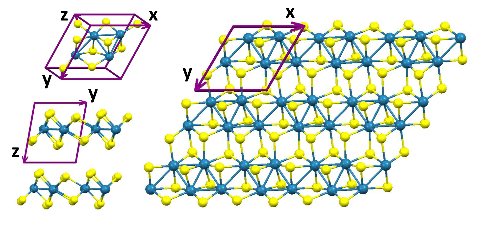
At the first step, we determined the equilibrium positions of the ions in the lattice by full self-consistent geometry optimization within DFT. The top and side views of the resulting structure are presented in Figure 1. The obtained lattice parameters and their comparison to experimental XRD data are given in the Supplementary.
At the second step, we employed two different DFT approaches (LDA and GGA) to calculate the three-dimensional band structure.
At the third step we calculated the diagonal components of the unit cell polarizability tensor via time dependent density functional theory (TDDFT) (see details in the Supplementary).
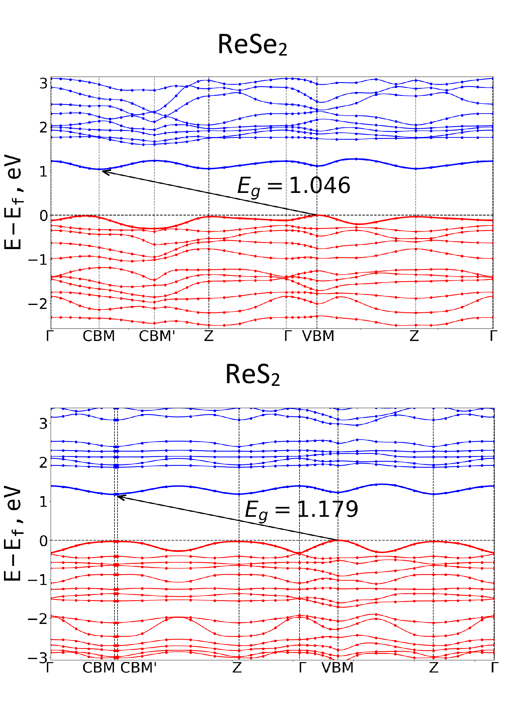
Most of the previous calculations of the band structure of the considered materials focused only on the dispersion along the special sets of directions, example being the 2D projection into the layers plane 13, 14. In the other cases, highly symmetric paths were chosen in the 3D BZ connecting three-dimensional special points, without exploring the structure of the whole BZ 15, 16 and thus missing the true band edges, which are crucially important for the determination of the optical response. The possible drawbacks of this approach were analyzed in detail in the recent work 10, where the necessity of the calculation of the band energies everywhere within the BZ and determination of the constant energy surfaces was stressed.
In the present paper we used the k-path, developed in Ref.10, and calculated the band structure using the following path: - CBM - CBM’ - Z - - VBM - VBM’ - Z - , where CBM - Conduction Band Minimum (LUMO), VBM - Valence Band Maximum (HOMO) and CBM’, VBM’ are the intersection points of the boundary surface of the Brillouin zone and the straight lines connecting and CBM or VBM points respectively. The paths from CBM’ or VBM’ points to the Z point run along the surface of the BZ containing Z point.
To find the k-points corresponding to the VBM and CBM we used the different grids in BZ - 6x6x6 and 7x7x7. The calculated values of the direct and indirect band gap are presented in Table 1 and compared with previously reported data 10, 15.
| LDA/GGA | LDA 10/GGA 10 | GGA+GW 15 | |
|---|---|---|---|
| indirect | 1.0043/1.0463 | 0.87/0.99 | - |
| direct (Z) | 1.0714/1.0909 | 0.97/1.00 | 1.38 |
| direct () | 1.3262/1.3421 | - | - |
| indirect | 1.1424/1.1790 | - | - |
| direct (Z) | 1.1908/1.2147 | - | 1.60 |
| direct () | 1.6809/1.7441 | - | 1.88 |
The obtained band structures of and are presented in Figure 2. It can be seen, that the energy of the lowest conduction and the highest valence bands depend only weakly on the wavevector, and the bands are close to the flat ones.
3.1 Optical response
In order to get the the optical response we employ the TDDFT approach, calculating the diagonal terms of the unit cell polarizability . The average dielectric susceptibility was found as the ratio of the polarization and the unit cell volume , . The dielectric permittivity was then found as . The spectra of the dielectric permittivities are shown in Fig. 3.
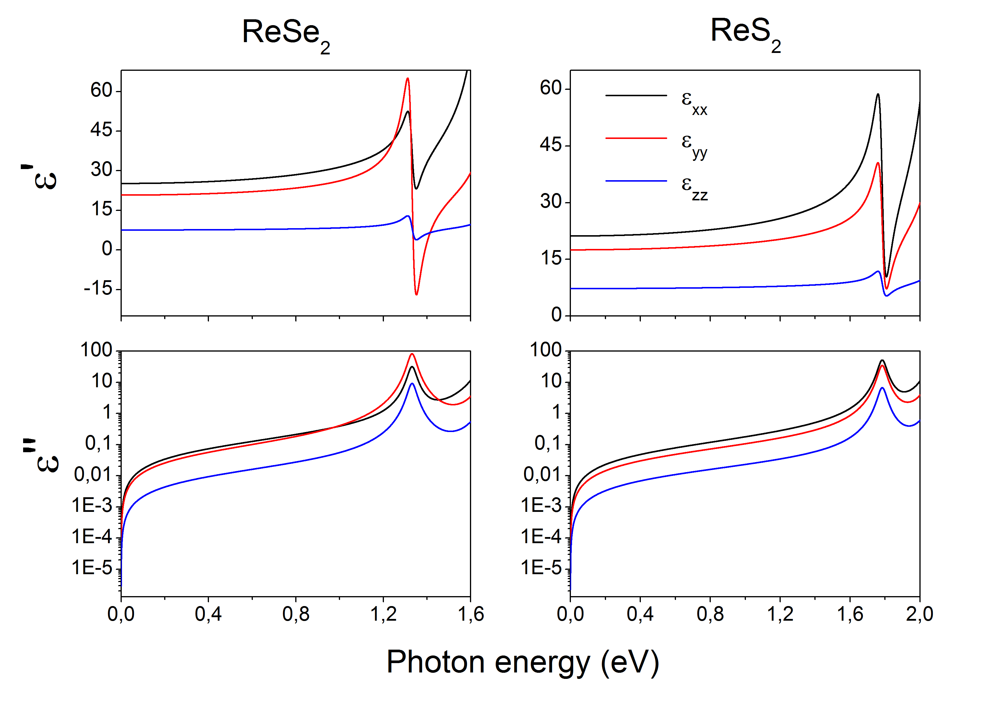
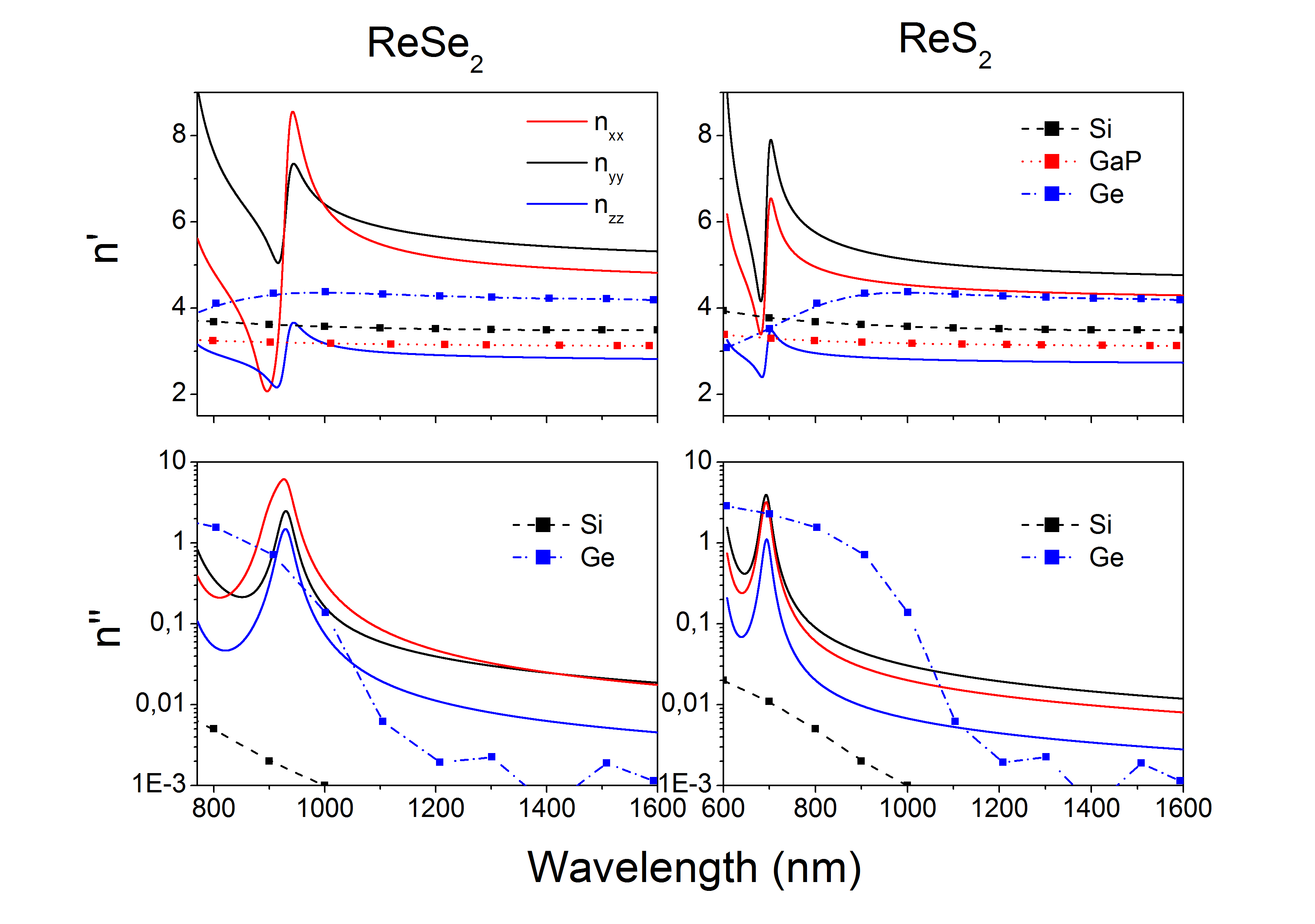
It can be seen that for both ReSe2 and ReS2 the absorption sharply increases only when the photon frequency approaches the band gap in point, 1.32 and 1.7 eV, respectively. Furthermore, we observe strong biaxial anisotropy for both crystals, stemming both from the layered structure of the material and reduced in-plane symmetry of the rhenium dichalcogenides 17. Noteworthy, large refractive index contrast and strong uniaxial anisotropy has been recently experimentally measured in bulk transition metal dichalcogenides 18, 19, 20 and hexagonal boron nitride 21. The pronounced biaxial anisotropy may be used for the the observation of the Dyakonov surface waves 22 in the rhenium dichalcogenide waveguides. One can see that the real parts of the in-plane components of the permittivity of ReSe2 exceed 25 in broad frequency range, which should correspond to high refractive index. Since for biaxial crystals the refractive index depends on the light propagation direction, we limit ourselves to the case when light travels along one of the three principal axes. In this case, the refractive index for each of the two polarizations is just a square root of the corresponding permittivity. The spectra of the refractive index components is shown in Fig. 4. One sees that in broad wavelengths range the refractive index exceeds 5 which is substantially larger that the index of the modern state of the art high-index materials such as c-Si 23, GaP 24 and Ge 25. The refractive index of ReS2 is smaller than that for ReSe2, but is still quite large. It should be noted that the imaginary part of the refractive index in this wavelengths range is negligibly small.
In our analysis, we have not accounted for the excitonic contribution to the dielectric permittivity, which can be substantial and would lead to the additional absorption losses at the frequencies slightly below the band gap. Nevertheless, since the range of large refractive index covers more than 0.5 eV below the band gap, it should be possible to detune from the exciton absorption lines to probe the lossless large refractive index.
Conclusions We established simple quantitative criterium for the search of high refrective index dielectric materials, expressed in terms of the single dimensionless parameter calculated as the ratio of the sum of the widths of conduction and valence bands and the bandgap. With the use of it, we found that ReSe2 is low loss material, possessing record high refractive index in a wide frequency range around 1 eV. Our conclusion is supported by the results of the DFT simulation of the optical response. Since currently there exist wast material databases containing the data on their bandstructures, the proposed criterion can be used for the automated search of the perspective candidates for the novel high-index materials for all-dielectric photonics.
4 Acknowledgement
This work was supported by the Ministry of Science and Higher Education of Russian Federation, goszadanie no. 2019-1246. The authors acknowledge the support from the mega-grant No. 14.Y26.31.0015 of the Ministry of Education and Science of the Russian Federation. I.A.S. acknowledges the support from the Icelandic research fund, grant No. 163082-051.
This material is available free of charge via the Internet at http://pubs.acs.org.
References
- Kuznetsov et al. 2016 Kuznetsov, A. I.; Miroshnichenko, A. E.; Brongersma, M. L.; Kivshar, Y. S.; Luk’yanchuk, B. Optically resonant dielectric nanostructures. Science 2016, 354
- Kivshar 2018 Kivshar, Y. All-dielectric meta-optics and non-linear nanophotonics. National Science Review 2018, 5, 144–158
- Mie 1908 Mie, G. Beiträge zur Optik trüber Medien, speziell kolloidaler Metallösungen. Annalen der physik 1908, 330, 377–445
- Kuznetsov et al. 2012 Kuznetsov, A. I.; Miroshnichenko, A. E.; Fu, Y. H.; Zhang, J.; Luk’Yanchuk, B. Magnetic light. Scientific reports 2012, 2, 492
- Decker et al. 2015 Decker, M.; Staude, I.; Falkner, M.; Dominguez, J.; Neshev, D. N.; Brener, I.; Pertsch, T.; Kivshar, Y. S. High-efficiency dielectric Huygens’ surfaces. Advanced Optical Materials 2015, 3, 813–820
- Arbabi et al. 2015 Arbabi, A.; Horie, Y.; Bagheri, M.; Faraon, A. Dielectric metasurfaces for complete control of phase and polarization with subwavelength spatial resolution and high transmission. Nature nanotechnology 2015, 10, 937–943
- Jahani and Jacob 2016 Jahani, S.; Jacob, Z. All-dielectric metamaterials. Nature nanotechnology 2016, 11, 23–36
- Shcherbakov et al. 2015 Shcherbakov, M. R.; Vabishchevich, P. P.; Shorokhov, A. S.; Chong, K. E.; Choi, D.-Y.; Staude, I.; Miroshnichenko, A. E.; Neshev, D. N.; Fedyanin, A. A.; Kivshar, Y. S. Ultrafast all-optical switching with magnetic resonances in nonlinear dielectric nanostructures. Nano letters 2015, 15, 6985–6990
- Schlickriede et al. 2020 Schlickriede, C.; Kruk, S. S.; Wang, L.; Sain, B.; Kivshar, Y.; Zentgraf, T. Nonlinear imaging with all-dielectric metasurfaces. Nano Letters 2020,
- Gunasekera et al. 2018 Gunasekera, S. M.; Wolverson, D.; Hart, L. S.; Mucha-Kruczynski, M. Electronic Band Structure of Rhenium Dichalcogenides. Journal of Electronic Materials 2018, 47, 4314–4320
- Zhao et al. 2015 Zhao, H.; Wu, J.; Zhong, H.; Guo, Q.; Wang, X.; Xia, F.; Yang, L.; Tan, P.; Wang, H. Interlayer interactions in anisotropic atomically thin rhenium diselenide. Nano Research 2015, 8, 3651–3661
- Giannozzi et al. 2009 Giannozzi, P. et al. QUANTUM ESPRESSO: a modular and open-source software project for quantum simulations of materials. Journal of Physics: Condensed Matter 2009, 21, 395502
- Dileep et al. 2016 Dileep, K.; Sahu, R.; Sarkar, S.; Peter, S. C.; Datta, R. Layer specific optical band gap measurement at nanoscale in MoS2 and ReS2 van der Waals compounds by high resolution electron energy loss spectroscopy. Journal of Applied Physics 2016, 119, 114309
- Wen et al. 2017 Wen, W. et al. Anisotropic Spectroscopy and Electrical Properties of 2D ReS2(1–x)Se2x Alloys with Distorted 1T Structure. Small 2017, 13, 1603788
- Echeverry and Gerber 2018 Echeverry, J. P.; Gerber, I. C. Theoretical investigations of the anisotropic optical properties of distorted and monolayers, bilayers, and in the bulk limit. Phys. Rev. B 2018, 97, 075123
- Arora et al. 2017 Arora, A.; Noky, J.; Drüppel, M.; Jariwala, B.; Deilmann, T.; Schneider, R.; Schmidt, R.; Del Pozo-Zamudio, O.; Stiehm, T.; Bhattacharya, A.; Krüger, P.; Michaelis de Vasconcellos, S.; Rohlfing, M.; Bratschitsch, R. Highly Anisotropic in-Plane Excitons in Atomically Thin and Bulklike ReSe2. Nano Letters 2017, 17, 3202–3207, PMID: 28414459
- Tian et al. 2016 Tian, H.; Tice, J.; Fei, R.; Tran, V.; Yan, X.; Yang, L.; Wang, H. Low-symmetry two-dimensional materials for electronic and photonic applications. Nano Today 2016, 11, 763–777
- Verre et al. 2019 Verre, R.; Baranov, D. G.; Munkhbat, B.; Cuadra, J.; Käll, M.; Shegai, T. Transition metal dichalcogenide nanodisks as high-index dielectric Mie nanoresonators. Nature nanotechnology 2019, 14, 679–683
- Busschaert et al. 2020 Busschaert, S.; Reimann, R.; Cavigelli, M.; Khelifa, R.; Jain, A.; Novotny, L. TMDC Resonators for Second Harmonic Signal Enhancement. arXiv preprint arXiv:2005.00894 2020,
- Ermolaev et al. 2020 Ermolaev, G.; Grudinin, D.; Stebunov, Y.; Kravets, V.; Duan, J.; Tselikov, G.; Voronin, K.; Yakubovsky, D.; Novikov, S.; Baranov, D., et al. Giant optical anisotropy in transition metal dichalcogenides for next-generation photonics. arXiv preprint arXiv:2006.00884 2020,
- Segura et al. 2018 Segura, A.; Artús, L.; Cuscó, R.; Taniguchi, T.; Cassabois, G.; Gil, B. Natural optical anisotropy of h-BN: Highest giant birefringence in a bulk crystal through the mid-infrared to ultraviolet range. Phys. Rev. Materials 2018, 2, 024001
- D’yakonov 1988 D’yakonov, M. New type of electromagnetic wave propagating at an interface. Sov. Phys. JETP 1988, 67, 714–716
- Philipp and Taft 1960 Philipp, H. R.; Taft, E. A. Optical Constants of Silicon in the Region 1 to 10 ev. Phys. Rev. 1960, 120, 37–38
- Adachi 1989 Adachi, S. Optical dispersion relations for GaP, GaAs, GaSb, InP, InAs, InSb, Journal of Applied Physics 1989, 66, 6030–6040
- Jellison Jr 1992 Jellison Jr, G. Optical functions of GaAs, GaP, and Ge determined by two-channel polarization modulation ellipsometry. Optical Materials 1992, 1, 151–160