current address: ]Lumileds Lighting Co., San Jose, CA 95131 USA.
Supplementary Information for “In Situ Microbeam Surface X-ray Scattering Reveals Alternating Step Kinetics During Crystal Growth”
Supplementary Methods 1:
X-ray Scattering
To characterize the behavior of and steps on a GaN single crystal (0001) surfaces, we performed in situ measurements of the CTRs during growth and evaporation in the OMVPE environment. For details on the GaN single crystal substrate, see vendor website (GANKIBANTM from SixPoint Materials, Inc., spmaterials.com). We used a chamber and goniometer at the Advanced Photon Source beamline 12ID-D which were designed for in situ surface X-ray scattering studies during growth Ju et al. (2017). For these experiments we used a modified chamber which had Be entrance and exit windows. A micron-scale X-ray beam illuminated a small surface area having a uniform step azimuth. To obtain sufficient signal, we used a wide-bandwidth “pink” beam setup similar to that described previously Ju et al. (2018, 2019). The beam incident on the sample had a typical intensity of photons per second at keV, in a spot size of m. At the incidence angle, this illuminated an area of m. X-ray scattering patterns were recorded using a photon counting area detector with a GaAs sensor having 512 512 pixels, 55 m pixel size, located m from the sample (Amsterdam Scientific Instruments LynX 1800). Slits downstream of the exit window block the scattering from the windows from reaching the region of the detector used to collect the CTR signal.
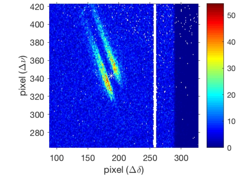
To process the X-ray data from the area detector, raw images were first corrected for detector flatfield, eliminating pixels with excessive noise, and the signal was normalized to the incident intensity. Supplementary Fig. 1 shows a typical corrected detector image, with streaks from the and CTRs. Because of the energy bandwidth of the pink beam Ju et al. (2019), the CTRs are broadened radially as well as being extended in the surface normal direction. To convert the images along an scan to reciprocal space, the coordinates of each pixel in each image were first calculated. The out-of-plane coordinate or varies across each image, following the Ewald sphere. The in-plane coordinates and were converted to in-plane radial and transverse components and relative to the central position. The intensities and values of each image were interpolated onto a fixed grid of and . We then interpolated the sequence of intensities from the scan at each and onto a grid of fixed values.
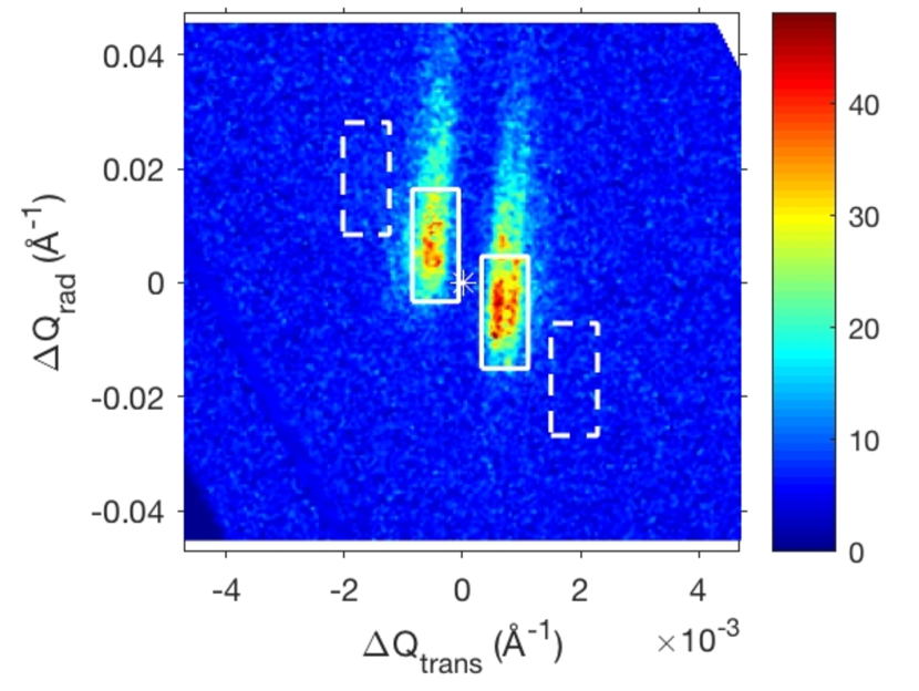
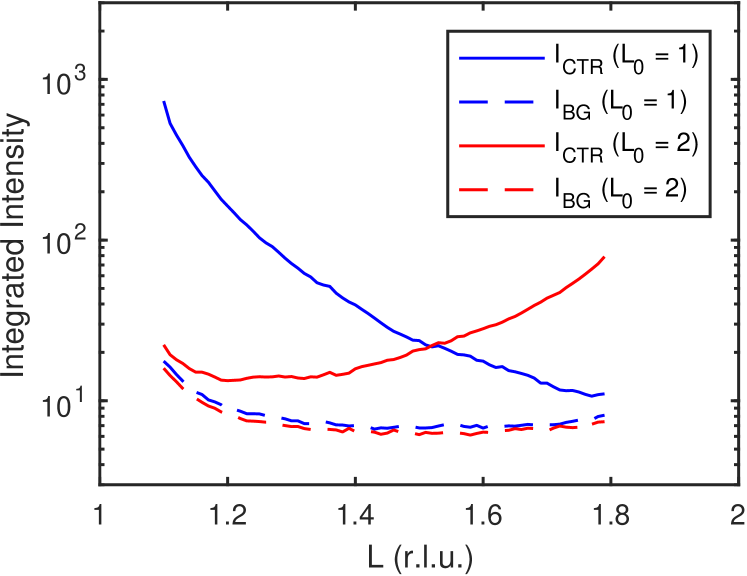
Supplementary Fig. 2 shows a typical cut through reciprocal space at fixed . The peaks from the and CTRs are conveniently separated in because of the deviation of the step azimuth from ; if the deviation had been zero, the peaks would have overlapped at because of the broadening in . Regions of and surrounding each CTR were defined to integrate the total intensity, with positions that vary with to follow the CTRs. Likewise adjacent regions were defined to integrate an equivalent volume of background scattering. Such regions are shown as solid and dashed rectangles, respectively, in Supplementary Fig. 2. Supplementary Fig. 3 shows the mean total CTR intensities and backgrounds in these regions as a function of for the scan between and for condition 4. The net CTR intensity was calculated by subtracting the background from the total for that CTR. We ran scans from to , to , and to on the and CTRs, skipping over the Bragg peaks to avoiding having the high intensity strike the detector. The range covered on each CTR varied depending upon the region covered by the detector in reciprocal space during the scan.
In order to determine whether exposure to the X-ray beam was affecting the OMVPE growth process, we periodically scanned the sample position while monitoring the CTR intensity. For the conditions reported here, there was no indication that the spot which had been illuminated differed in any way from the neighboring regions. During growth at higher temperatures (e.g. K), we did observe local effects of the X-ray beam on the surface morphology.
Supplementary Methods 2:
Net Growth Rates
Under the OMVPE conditions used, we observe that deposition of GaN is Ga transport limited (i.e. the deposition rate is proportional to the TEGa supply rate, nearly independent of and NH3 supply), and the net growth rate has a negative offset at zero TEGa supply corresponding to an evaporation rate that depends on and the carrier gas composition (e.g. presence or absence of H2). To determine the deposition rate for the conditions used in the X-ray study, we used the deposition efficiency (deposition rate per TEGa supply rate) determined from previous studies of CTR oscillations during layer-by-layer growth Perret et al. (2014); Ju et al. (2019). We also measured the evaporation rates at two higher temperatures and both carrier gas compositions (0% and 50% H2), and extrapolated them to the lower temperatures studied here.
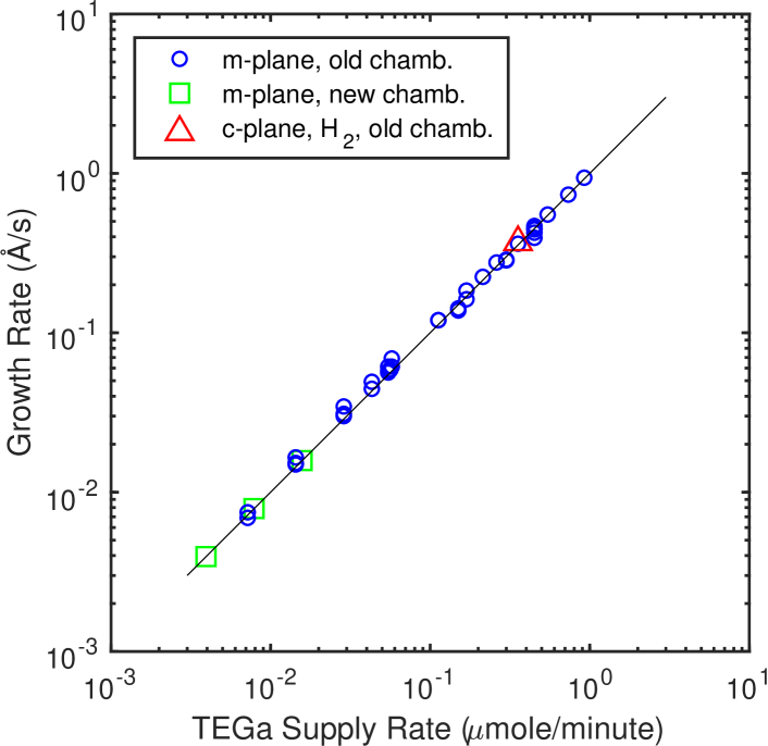
Supplementary Fig. 4 shows the growth rates measured from CTR oscillations during layer-by-layer growth as a function of TEGa supply Perret et al. (2014); Ju et al. (2019). In all cases the chamber flows were the same as in the X-ray study reported here (e.g. 2.7 slpm NH3, 267 mbar total pressure). Almost all data points are for growth on m-plane GaN in N2 carrier gas (0% H2), which exhibits layer-by-layer mode over a wide range of conditions. Data are shown from both a previous growth chamber (“old” chamber) Stephenson et al. (1999) and the current growth chamber (“new” chamber) Ju et al. (2017, 2019). The two chambers were designed to have the same flow geometry, and the growth behavior of both appear to be identical. The data points from the previous chamber range in temperature from K to K; the data points for the current chamber are for K. The line shown is a fit to the data from the current chamber, which gives a deposition efficiency of 1.0 (Å s-1)/(mole min-1). One data point is shown for growth on c-plane (0001) GaN in 50% N2 + 50% H2 carrier gas at K; layer-by-layer growth was only observed on (0001) GaN under this condition. It agrees with the m-plane data obtained in 0% H2 carrier, suggesting that the same deposition efficiency can be used for (0001) GaN in either 0% or 50% H2 carrier gas. We expect that there is negligible evaporation at K in either carrier gas.
To estimate the evaporation rate at the temperatures used in the X-ray study presented here (e.g. K), we used laser interferometry to observe the change in thickness of an (0001) GaN film on a sapphire substrate Ju et al. (2017); Koleske et al. (2005), under conditions of zero TEGa flow at higher . As the film thickness changes during growth or evaporation, the back-scattered laser intensity oscillates with time due to interference between light reflected from the film surface and the substrate/film interface, according to
| (1) |
where and are the envelope of the minima and maxima, which can vary with time as film roughness changes, and the thickness oscillation period is , where Å is the wavelength of the light and is the refractive index of GaN. This can be inverted to obtain the thickness evolution as
| (2) |
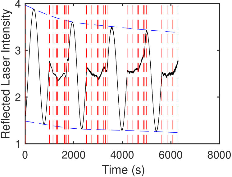
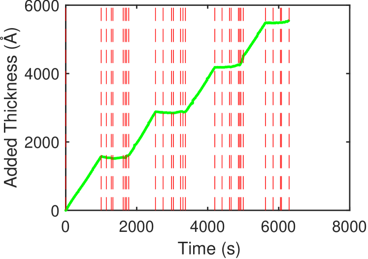
Supplementary Fig. 5 shows the evolution of the laser signal with time during the experiment. We began by growing a full oscillation at a high growth rate to obtain initial values for and . Once the signal had reach a value intermediate between these limits, where the phase of the oscillation is most accurately determined, we changed the TEGa flow to observe the net growth or evaporation rate at some fixed values of . Then we changed and/or the carrier gas concentration, and repeated the process starting with growing a full oscillation at a high rate. The blue dashed curves in Supplementary Fig. 5 show the interpolated and envelopes. Supplementary Fig. 6 shows the thickness change with time extracted with Supplementary Eq. (2), using a value of Å corresponding to Tapping and Reilly (1986); Touloulian et al. (1977). Supplementary Fig. 7 shows expanded regions of the thickness evolution, where we varied for specific and H2 fractions. The solid lines show linear fits to extract the net growth rate in Å s-1 at each value of . This is equal to , where is the growth rate in ML s-1 and is the thickness of a monolayer (ML).
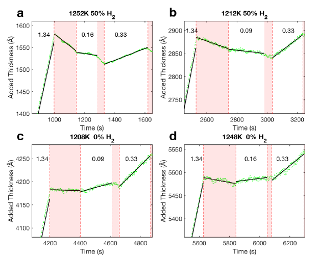
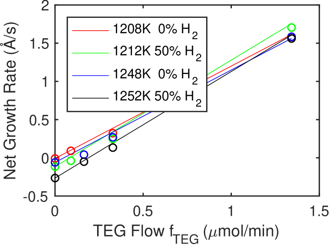
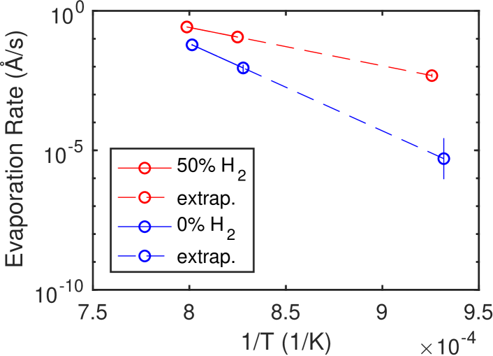
The extracted values of are given in Supplementary Table 1 and plotted in Supplementary Fig. 8 as a function of . We observe that becomes negative at due to evaporation, and that evaporation is more rapid at higher and when H2 is present in the carrier gas. These evaporation rates in 50% H2 are consistent with the rate of m-2s-1 or Å s-1 given in the literature Koleske et al. (2001) at a higher K with H2 and NH3 at a total pressure of mbar. Also given in Supplementary Table 1 are the deposition efficiencies obtained from linear fits to at the four values of for each and H2 fraction. The values are all similar to but slightly higher than the value of (Å s-1)/(mole min-1) that we have observed from growth oscillations during layer-by-layer growth at lower , described above Ju et al. (2019); Perret et al. (2014). The efficiency seems to be slightly larger for 50% H2 compared with 0% H2. This may indicate that the deposition efficiency can vary somewhat as the flow and diffusion fields vary in the chamber with or carrier gas composition.
To obtain the evaporation rate at the lower used in the X-ray experiments, we extrapolated the values at for 50% H2 or 0% H2 assuming Arrhenius behavior of the evaporation rate, as shown in Supplementary Fig. 9. The fitted activation energies are and eV in 50% and 0% H2, respectively. We obtain evaporation rates of Å s-1 at K with 50% H2, and Å s-1 (with error limits of a factor of 5) at K with 0% H2. We have used these evaporation rates, as well as the low-temperature deposition efficiency of (Å s-1)/(mole min-1) and the TEGa flow rates of or mole min-1, to calculate the net growth rates given in Table I in the main text for the 4 conditions studied.
| H2 | ||||
| (K) | in | (mole | (Å s-1) | (Å s-1)/ |
| carr. | min-1) | (mole min-1) | ||
| 1208 | 0% | 0.00 | ||
| 0.09 | ||||
| 0.33 | ||||
| 1.34 | ||||
| 1212 | 50% | 0.00 | ||
| 0.09 | ||||
| 0.33 | ||||
| 1.34 | ||||
| 1248 | 0% | 0.00 | ||
| 0.16 | ||||
| 0.33 | ||||
| 1.34 | ||||
| 1252 | 50% | 0.00 | ||
| 0.16 | ||||
| 0.33 | ||||
| 1.34 |
Supplementary Discussion 1:
Chemical potentials in OMVPE
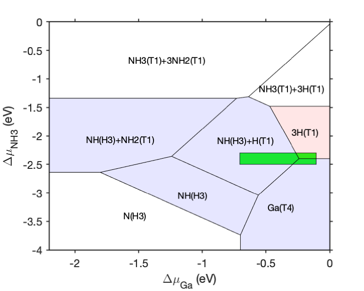
To calculate the CTR intensities to fit to the experimental profiles, we need to include the effect of reconstruction of the surface. The relaxed atomic structures and free energies of various surface reconstructions for GaN (0001) in the OMVPE environment containing NH3 and H2 have been calculated Van de Walle and Neugebauer (2002a); Walkosz et al. (2012), leading to a phase diagram that can be expressed in terms of the chemical potentials of Ga and NH3 Van de Walle and Neugebauer (2002b); Walkosz et al. (2012). In this section we estimate these chemical potentials from the conditions in our experiments, to locate the appropriate region of the phase diagram and identify the predicted reconstructions in this region.
Supplementary Fig. 10 shows the predicted surface phase diagram Walkosz et al. (2012). The vertical axis is the chemical potential of NH3 relative to its value at K. This can be expressed as
| (3) |
where is the free energy of NH3 gas at a pressure of 1 bar obtained from thermochemical tables Chase (1998), and is the partial pressure of NH3 in the experiment. These can be evaluated at the experimental conditions. For K, the tables give eV. Thus for bar, one obtains eV.
The horizontal axis in Supplementary Fig. 10 is the chemical potential of Ga relative elemental liquid Ga. This can be related to the activity of N2 using
| (4) |
where is the free energy of formation of GaN from liquid Ga and N2 gas at 1 bar, and is the activity (effective partial pressure) of N2.
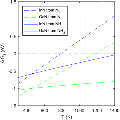
In OMVPE, a chemically active precursor such as ammonia is typically used to provide the high nitrogen activity required to grow group III nitrides. The need for this can be seen in Supplementary Fig. 11, which shows the free energies of the reactions to form GaN and InN from the condensed metallic elements and either vapor N2 or vapor NH3 at 1 bar Chase (1998); Ambacher et al. (1996). At typical temperatures used for growth of high quality single crystal films at high rates (e.g. 1000 K for InN, 1300 K for GaN), the formation energy from N2 is positive, indicating that the nitride is not stable and cannot be grown from N2 at 1 bar. In contrast, the formation energies of the nitrides (plus H2 at 1 bar) from the metals and NH3 are negative at all relevant growth temperatures, indicating that growth from 1 bar of NH3 is possible.
However, actual OMVPE conditions do not correspond with equilibrium, because the very high partial pressures of N2 and/or H2 that would correspond to equilibrium with NH3 at these temperatures are not allowed to accumulate. Thus, while formation of InN and GaN from NH3 is energetically favored under OMVPE conditions, decomposition of these nitrides into N2 is also energetically favored. This metastability is manifested in the oscillatory growth and decomposition of InN that has been observed Jiang et al. (2008). Thus the kinetics of the reaction steps that determine the nitrogen activity at the growth surface are critical to understanding and controlling OMPVE growth of metastable nitrides.
In previous work we have measured the trimethylindium (TMI) partial pressures required to condense InN and elemental In onto GaN (0001) Jiang et al. (2008). They can be analyzed to give experimentally determined values for the effective surface nitrogen activity arising from NH3 under OMVPE conditions. The experiments were carried out using a very similar growth chamber Stephenson et al. (1999) as that used for the in situ X-ray studies described below, using the same a total pressure of 0.267 bar, and the same NH3 and carrier flows (2.7 standard liters per minute (slpm) NH3 and 1.1 slpm N2 in the group V channel, 0.9 slpm N2 carrier gas for TMI in the group III channel). We have performed chamber flow modeling to calculate the equivalent TMI and NH3 partial pressures and above the center of the substrate surface as a function of inlet flows. At typical growth temperatures, an inlet flow of 0.184 mole min-1 TMI corresponds to bar, and an inlet flow of 2.7 slpm NH3 corresponds to bar.
| Quantity | Value as (K) |
|---|---|
| (eV) | |
| Ambacher et al. (1996) | |
| Ambacher et al. (1996) | |
| Jiang et al. (2008) | |
| Jiang et al. (2008) | |
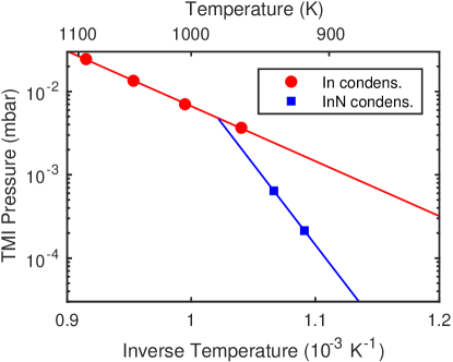
Supplementary Fig. 12 shows the - boundaries determined by in situ X-ray fluorescence and diffraction measurements for initial condensation of elemental In liquid or crystalline InN onto a GaN (0001) surface at bar Jiang et al. (2008). At TMI partial pressures above the boundaries shown, the condensed phases nucleate and grow on the surface; at lower , the condensed phases evaporate. The InN and In condensation boundaries intersect at 979 K.
A relationship between the nitrogen and indium activities at the InN condensation boundary can be obtained from the equilibrium
| (5) |
which gives the chemical potential expression
| (6) |
and the activity expression
| (7) |
where is the formation energy of InN from liquid In and N2 at 1 bar shown in Supplementary Fig. 12. We assume that the activity of In relative to liquid In at the InN boundary is equal to the ratio , giving
| (8) |
at the experimental condition, bar. Supplementary Eq. (7) can then be used to obtain the nitrogen activity relative to 1 bar (i.e. effective partial pressure of N2 in bar) for bar.
Supplementary Table 2 summarizes the calculations to obtain the nitrogen activity and under our OMVPE conditions. The value of eV at the experimental temperature K gives the horizontal coordinate on the phase diagram from Supplementary Eq. (4) as eV. The value of eV at the experimental temperature K gives the vertical coordinate on the phase diagram from Supplementary Eq. (3) as eV. This position is shown on the predicted surface phase diagram, Supplementary Fig. 10, with a rectangle representing the relatively large uncertainty in .
A recent study of reconstructions on GaN (0001) in the OMVPE environment Kempisty and Kangawa (2019) included the effects of additional entropy associated with adsorbed species, which leads to a phase diagram that varies somewhat with temperature, even when expressed in chemical potential coordinates. These effects tend to stabilize reconstructions with H adsorbates at higher , giving a larger region of phase stability for the 3H(T1) reconstruction than shown in Supplementary Fig. 10. This is consistent with our finding that the 3H(T1) reconstruction agrees best with the experimental CTRs for all conditions studied.
Supplementary Discussion 2:
Kink Density
The density of kinks on a step is determined by two terms: the minimum density that is geometrically required to give the average direction of the step, and the additional thermally generated kink pairs Burton et al. (1951). This can be analyzed in terms of the probabilities and for positive or negative kinks to occur at each lattice site on the step. For a close-packed surface with lattice parameter , the geometrical requirement gives
| (9) |
where is the angle of the step with respect to the atomic rows in the type directions. The probabilities must also satisfy
| (10) |
where is the energy cost to generate a kink pair, and we assume the kink probabilities are much smaller than unity.
For our sample with and Å, the geometrically required maximum average kink spacing is Å. If we estimate the kink pair energy as where eV is the bulk binding energy per molecule for GaN Xu et al. (2017), this gives an average kink spacing of Å at K.
Acknowledgements.
Work supported by the U.S Department of Energy (DOE), Office of Science, Office of Basic Energy Sciences, Materials Science and Engineering Division. Experiments were performed at the Advanced Photon Source beamline 12ID-D, a DOE Office of Science user facility operated by Argonne National Laboratory.References
- Ju et al. (2017) Guangxu Ju, Matthew J. Highland, Angel Yanguas-Gil, Carol Thompson, Jeffrey A. Eastman, Hua Zhou, Sean M. Brennan, G. Brian Stephenson, and Paul H. Fuoss, “An instrument for in situ coherent X-ray studies of metal-organic vapor phase epitaxy of III-nitrides,” Rev. Sci. Instrum. 88, 035113 (2017).
- Ju et al. (2018) Guangxu Ju, Matthew J. Highland, Carol Thompson, Jeffrey A. Eastman, Paul H. Fuoss, Hua Zhou, Roger Dejus, and G. Brian Stephenson, “Characterization of the X-ray coherence properties of an undulator beamline at the Advanced Photon Source,” J. of Synchrotron Radiat. 25, 1036–1047 (2018).
- Ju et al. (2019) Guangxu Ju, Dongwei Xu, Matthew J. Highland, Carol Thompson, Hua Zhou, Jeffrey A. Eastman, Paul H. Fuoss, Peter Zapol, Hyunjung Kim, and G. Brian Stephenson, “Coherent X-ray spectroscopy reveals the persistence of island arrangements during layer-by-layer growth,” Nat. Phys. 15, 589–594 (2019).
- Perret et al. (2014) Edith Perret, M. J. Highland, G. B. Stephenson, S. K. Streiffer, P. Zapol, P. H. Fuoss, A. Munkholm, and Carol Thompson, “Real-time x-ray studies of crystal growth modes during metal-organic vapor phase epitaxy of GaN on c- and m-plane single crystals,” Appl. Phys. Lett. 105, 051602 (2014).
- Stephenson et al. (1999) G. B. Stephenson, J. A. Eastman, O. Auciello, A. Munkholm, Carol Thompson, P. H. Fuoss, P. Fini, S. P. DenBaars, and J. S. Speck, “Real-time x-ray scattering studies of surface structure during metalorganic chemical vapor deposition of GaN,” MRS Bull. 24[1], 21 (1999).
- Koleske et al. (2005) D. D. Koleske, M. E. Coltrin, and M. J. Russell, “Using optical reflectance to measure GaN nucleation layer decomposition layer kinetics,” J. Cryst. Growth 279, 37–54 (2005).
- Tapping and Reilly (1986) J. Tapping and M. L. Reilly, “Index of refraction of sapphire between 24 and 1060 C for wavelengths of 633 and 799 nm,” J. Opt. Soc. Am. A 3, 610–616 (1986).
- Touloulian et al. (1977) Y. S. Touloulian, R. K. Kirby, R. E. Taylor, and T. Y. Lee, Thermal Expansion: Nonmetallic Solids, Vol. 13 (Springer, 1977) pp. 154–389.
- Koleske et al. (2001) D. D. Koleske, A. E. Wickenden, R. L. Henry, Culbertson. J. C., and M. E. Twigg, “GaN decomposition in H2 and N2 at MOVPE temperatures and pressures,” J. Cryst. Growth 223, 466–483 (2001).
- Van de Walle and Neugebauer (2002a) Chris G. Van de Walle and J. Neugebauer, “First-principles surface phase diagram for hydrogen on GaN surfaces,” Phys. Rev. Lett. 88, 066103 (2002a).
- Walkosz et al. (2012) Weronika Walkosz, Peter Zapol, and G. Brian Stephenson, “Metallicity of InN and GaN surfaces exposed to NH3,” Phys. Rev. B 85, 033308 (2012).
- Van de Walle and Neugebauer (2002b) Chris G. Van de Walle and J. Neugebauer, “Role of hydrogen in surface reconstructions and growth of GaN,” J. Vac. Sci. Technol. B 20, 1640–1646 (2002b).
- Chase (1998) Malcolm W. Chase, Jr., “NIST-JANAF thermochemical tables (4th edition),” J. Phys. Chem. Ref. Data, Monograph 9 , 1–1151 (1998).
- Ambacher et al. (1996) O. Ambacher, M. S. Brandt, R. Dimitrov, T. Metzger, M. Stutzmann, R. A. Fischer, A. Miehr, A. Bergmaier, and G. Dollinger, “Thermal stability and desorption of Group III nitrides prepared by metal organic chemical vapor deposition,” J. Vac. Sci. Technol. B 14, 3532–3542 (1996).
- Jiang et al. (2008) Fan Jiang, A. Munkholm, R.-V. Wang, S. K. Streiffer, Carol Thompson, P. H. Fuoss, K. Latifi, K. R. Elder, and G. B. Stephenson, “Spontaneous oscillations and waves during chemical vapor deposition of InN,” Phys. Rev. Lett. 101, 086102 (2008), (See online supplemental for trimethylindium (TMI) partial pressures required to condense InN and elemental In).
- Kempisty and Kangawa (2019) Pawel Kempisty and Yoshihiro Kangawa, “Evolution of the free energy of the GaN (0001) surface based on first-principles phonon calculations,” Phys. Rev. B 100, 085304 (2019).
- Burton et al. (1951) W. Burton, N. Cabrera, and F. Frank, “The growth of crystals and the equilibrium structure of their surfaces,” Philos. Trans. Royal. Soc. London Ser. A 243, 299 (1951).
- Xu et al. (2017) Dongwei Xu, Peter Zapol, G. Brian Stephenson, and Carol Thompson, “Kinetic Monte Carlo simulations of GaN homoepitaxy on c- and m-plane surfaces,” J. Chem. Phys. 146, 144702 (2017).