Charge collection efficiency in back-illuminated Charge-Coupled Devices.
Abstract
Low noise CCDs fully-depleted up to 675 micrometers have been identified as a unique tool for Dark Matter searches and low energy neutrino physics. The charge collection efficiency (CCE) for these detectors is a critical parameter for the performance of future experiments. We present here a new technique to characterize CCE in back-illuminated CCDs based on soft X-rays. This technique is used to characterize two different detector designs. The results demonstrate the importance of the backside processing for detection near threshold, showing that a recombination layer of a few microns significantly distorts the low energy spectrum. The studies demonstrate that the region of partial charge collection can be reduced to less than 1 m thickness with adequate backside processing.
1 Thick Fully-Depleted CCDs for Dark Matter and neutrino experiments
Charged Coupled Devices (CCD) with low readout noise and large active volume have been identified among the most promising detector technologies for the low mass direct dark matter search experiments, probing electron and nuclear recoils from sub-GeV DM [1, 2, 3, 4, 5]. The recent development of the Skipper-CCD [6, 7] demonstrated the ability to measure ionization events with sub-electron noise extending the reach of this technology to unprecedented low energies. Experiments based on this technology are planned for the coming years with total CCD active mass going from 100 grams to several kilograms [8, 9]. At the same time the low noise CCD technology has been implemented in low energy neutrino experiments [10, 11] and are planned for future developments[12].
There are several key performance parameters for the CCD sensors in future developments that are part of a significant R&D effort for future projects [8, 9, 12]. The most important performance requirements are the pixel dark current [7], readout noise optimization [13], Fano factor [14] and charge transport in the sensor [15].
The Charge Collection Efficiency (CCE) is defined as the fraction of the total charge produced during a ionization event that is collected in the CCD pixel for later readout. For a fully depleted detector, with a large electric field, CCE is approximately 100% [16] for the full active volume. In regions of the detector with lower electric field, CCE could be less than 100% due to charge recombination. Regions of partial CCE distort the measured spectrum of ionization events, affecting energy calibration and particle identification.
Back illuminated CCDs in astronomy are treated to have a thin entrance window for light, with low reflectivity. This is specially important when detectors are used for wavelength shorter than 500 nm [17, 18, 19]. A 500 nm photon has an absorption length of 1 m in Silicon, and any layer with partial charge collection (PCC) on the back surface will degrade the detection efficiency for blue light. The measurements presented in Ref.[20] compare the detection efficiency for visible photons with the reflectivity. These studies show that all photons with wavelength longer than 500 nm are fully detected, unless they are reflected on the back surface. These results show that the bulk of the detector has 100% CCE, and that any recombination on these sensors occurs only on the first 1m near the back surface.
For thick CCDs, as those used in dark matter [1, 2, 3, 4, 5, 6, 7] and neutrino experiments [10, 11], a backside ohmic contact is required in order to apply the needed substrate bias to fully deplete sensor [21]. At the same time, different processing techniques are used on the backside to reduce dark current. The backside processing of these sensors determines the field shaping near the surface, and has a large impact in the CCE for events in that region. We study here the CCE for back-illuminated detectors with more than 200 m thickness.
2 Determination of the backside CCE using X-rays
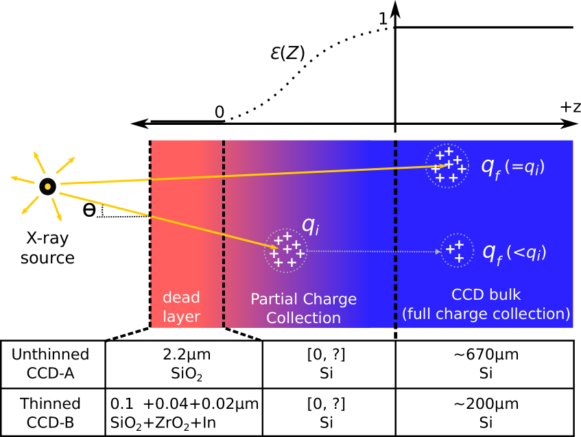
X-rays can be used to characterize the CCE near the back surface of a CCD. Figure 1 shows a cartoon of X-ray setup together with the most important variables that participate in the analysis. Some important aspects and definitions
-
•
The source emits photons with uniform angular distribution covering a full hemisphere. The angular distribution on the sensor depends on the geometry of the setup. We model the angular distribution by , where is measured as the angle of the incidence of the photon in the CCD compared to perpendicular direction to the back surface of the sensor.
-
•
The X-ray photons can reach the PCC layer and the bulk of the sensor volume. The interaction depth in the sensor depends on the incident angle and its probability distribution function (pdf) can be written as , where is the attenuation length of the photon.
-
•
X-rays produce an ionization charge packet with mean value , where is the energy of the photon and = 3.75 eV is the mean ionizing energy [14]. For now, we assume that the initial charge packet is the same for all photoelectric absorption events, we discuss later how the Fano noise affects the final results. The primary charge ionization is the same for the PCC layer and the bulk of the sensor as represented in Fig. 1.
-
•
is the CCE function in the backside of the detector. The function indicates the fraction of carriers that are collected by the pixel after drifting away from the PCC layer (carriers that do not recombine in the PCC layer). This function depends on the depth of the interaction. If the primary charge packet occurs deep in the PCC layer (far from the bulk of the sensor), carrier will have more time to recombine before they reach the bulk. Thus, increases monotonically.
-
•
is the charge that escapes from the PCC layer and can be collected and measured by the sensor. As illustrated in Fig. 1, this will depend on the interaction depth of the photon. We will refer as to the random variable accounting for the possible values of the X-ray events with pdf . The distribution of is the observable in our data.
From the previous definitions the measured charge can be expressed as
| (2.1) |
2.1 Determination of efficiency function using monochromatic X-ray source
The measured spectrum of events normalized by the total number of events () is an estimation of . We can then use it to estimate the cumulative distribution function (cdf) of :
where is such that , and
| (2.4) |
The measurements at low charge values are often affected by readout noise. In this case, we calculate the cdf integrating away from low charge values,
| (2.5) |
For each , we find such that where the efficiency is .
The method to calculate the CCE using one X-ray peak is summarized in the Table 2 of the Appendix.
2.2 Determination of efficiency function using an 55Fe source
55Fe X-ray source has an extensive use in the calibration of typical performance parameters of CCDs and other sensors [16]. In this article we extend its use to characterize the charge collection in the PCC layer using the methodology proposed in Section 2.1. The main characteristics of the three X-rays emitted by 55Fe are summarized in Table 1. X-rays have similar energy and attenuation length and therefore can be treated as a single X-ray line for the purpose of this analysis.
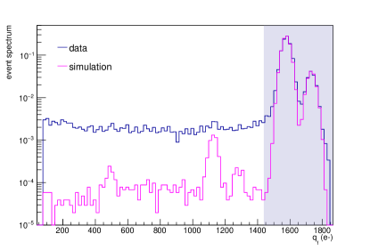
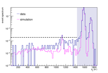
. XK Energy (keV) Mean e-h production () Intensity Attenuation length () 5887.65 1570 8.45 (14) 28.7 5898.75 1573 16.57 (27) 28.9 6490.45 1731 3.40 (7) 38.0
Then, pdf for the interaction as a function of depth are
and
for the and , respectively. With the same angular distribution in both cases.
where and , such that the depth cdf equals the measured cumulative distribution of events. and are the relative intensities determined by Table 1 normalized by the number of desintegrations. Since we assume a monotonically increasing function, then . Using a more condense notation
| (2.7) |
A recursive nonlinear numeric solver is used to find and simultaneously. Three features of the 55Fe source can be used to simplify the problem.
-
•
Larger -flux than -flux, since
-
•
is always greater than because of the difference in the attenuation length () and the fact that .
-
•
As becomes smaller than then becomes closer to , and therefore becomes closer to . In fact, and differ only 10%.
Most of the signal is dominated by the photon and a small effect is introduced by assuming a unique . This assumption allows to follow the same procedure presented in Section 2.1 to solve equation 2.7. Assuming the true collection efficiency at lays between and . A simple approximation is . The full method for an 55Fe source is summarized in Table 3, in the Appendix.
3 Experimental results
We study here two different CCDs.
CCD-A was designed by the LBNL Microsystems Laboratory [23] as part of the R&D effort for low energy neutrino experiments [10] and low mass direct dark matter search [3]. This is a rectangular CCD with 8 million square pixels of 15 m 15 m each. The CCD is fabricated in n-type substrate with a full thickness of 675 m. The resistivity of the substrate greater than 10000 -cm. The CCD is operated with 40V bias voltage that fully depletes the high-resistivity substrate using the method developed in Ref.[21]. In order to trap impurities that migrate during the sensor processing, a 1m thick in-situ doped polysilicon (ISDP) layer is deposited on the backside of the detector. This layer plays a critical role controlling the dark current of the detector. Additional layers of silicon nitride, phosphorous-doped polysilicon and silicon dioxide are added to the backside ( 2 m total thickness). Phosphorous can migrate into the high resistivity material producing a region of a few microns where charge can recombine before drifting to the collecting gates of the detector. This region constitutes the PCC layer that we characterize with 55Fe X-rays, as shown in Figure 1.
CCD-B is similar to CCD-A with a few important differences. The detector has 4 million pixels, with a thickness of 200 m. It is also fabricated in high resistivity n-type silicon. The backside of the sensor has been processed for astronomical imaging. A backside ohmic contact is formed by low-pressure, chemical-vapor deposition in-situ doped polycrystalline silicon (ISDP). This layer is made thin for good blue response, typically 10-20 nm, and is robust to over-depleted operation that is necessary to guarantee full depletion across the entire CCD. This detector is operated at bias voltage of 40 V. Because of its backside treatment, this detector is not expected to have significant charge recombination near the back surface. The detector is exposed to 55Fe X-rays on the backside, as shown in Figure 1.
The 55Fe was located 3.55 cm away from the CCDs. The effective depth distribution of interacting photons was calculated using a Monte Carlo simulation, and the result is
| (3.1) |
where () represents the intensity and () is the effective optical depth for the () spectral line. , , m, and m.
3.1 Results for CCD-A
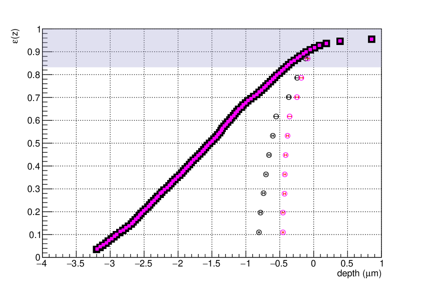
The spectrum of measured charge for CCD-A is shown in the top panel of Fig. 2, and compared with a Geant4[24] simulation assuming perfect CCE for the entire volume of the sensor (). The Kα and Kβ peaks from Table 1 are evident. The excess of reconstructed events to the left of these peaks is attributed to the PCC layer, where charge recombination produces a measurement below the peak energy. The bump in the simulation around 1100 e- is an escape peak, as discussed in Ref.[25]. This data is used to measure the CCE function following the prescription in Section 2.2, and the results are shown in the top panel of Fig.3. The depth scale is chosen such that . The shaded region corresponds to the energies between 5.4 keV and 7 keV where the events from and are dominant and systematic uncertainties are expected to be important. In this region the precise shape of curve is less reliable.
3.2 Results for CCD-B
The spectrum of measured charge for CCD-B is shown in the bottom panel of Fig.2, and compared with a Geant4 [24] simulation with perfect CCE. As for CCD-A, the Kα and Kβ spectral lines are evident, CCD-B has a different output stage producing higher resolution peaks [6]. The relative rate of events on the left of the peaks, are well below the rate observed for CCD-A and consistent with the simulation. These events are produced mostly by low probability Compton scattering of X-rays. The CCE function is determined as discussed in Section 2.2 and the results are shown in Fig.3 bottom panel, black circles. The measurement of is also performed after the predicted Compton spectrum is subtracted based on the simulation, the results are shown in bottom panel of Fig.3, magenta circles. As before, the horizontal axis is selected such that .
3.3 Conclusion
The results of CCD-A and CCD-B showed in Fig.3 demonstrate the large impact that the backside processing could have in the CCE for back-illuminated detectors. When a layer of a few microns with charge recombination is present on the CCD, the spectrum for low energy X-rays gets significantly distorted. The charge recombination generates a significant number of lower energy events in the spectrum. The backside processing performed in detectors optimized for astronomical instruments eliminates this issue for the most part, as shown with CCD-B. The generation of low energy events constitute a major concern for experiments looking for rare signals near the detector threshold [1, 2, 3, 4, 5, 6, 7, 10, 11].
The results obtained here for CCD-B, optimized for astronomical imaging, are consistent with the observations of detection efficiency and reflectivity in Ref.[20].
A new technique was introduced here to characterize the CCE for back-illuminated CCDs, this technique can easily be generalized to other semiconductor detectors. The technique uses tools that are commonly available at the detector characterization laboratories. As shown here, the new method is capable of measuring a PCC layer of a few micrometers. The sensitivity to a very thin PCC layer is limited by the energy of the 55Fe X-rays, and the technique could be easily extended for much thinner recombination layers using lower energy X-rays. This technique will be a powerful tool in the optimization of detectors for the next generation of low threshold experiments looking for rare events such as dark matter, or coherent neutrino nucleus scattering[9, 12].
Appendix: Details of the method
The details of the method to measure the CCE in the backside of a back-illuminated CCD are presented in Table 2. The details of method used with the 55Fe source having two X-ray lines is presented in Table 3.
| 1) Calculate angular distribution of incident photons: |
| Based on the geometry of the experiment evaluate . |
| 2) Calculate depth distribution of events: |
| , where is the attenuation length of the photon. Then, calculate the cdf (or from Eq. (2.5)). |
| 3) Make a spectrum of measured events: |
| Calculate the spectrum of events reconstructed from the data and normalize it by total number of events (). This is the estimation . |
| 4) Calculate integral of the measured spectrum up to a charge : |
| Calculate cdf either (from Eq. 2.2), or (from Eq. 2.5). |
| 5) Find : |
| Find that equals the cdf of the interaction depth with the cumulative proportion of measured events. This is , or . |
| 6) Calculate the efficiency at : |
| . |
| 7) Repeat steps 4, 5 and 6 for a different to complete . |
| 1) Calculate angular distribution of incident photons: |
| Based on the geometry of the experiment evaluate . |
| 2) Calculate depth distribution of events: |
| , where is the attenuation length of the photon. Then, calculate the cumulative distribution (or from equation 2.5). |
| 3) Make an spectrum of measured events: |
| Calculate the spectrum of events reconstructed from the data and normalize it by total number of events (). This is the estimation . |
| 4) Calculate integral of the measured spectrum up to a charge : |
| Calculate cumulative distributions either (from Eq. 2.2), or (from Eq. 2.5). |
| 5) Find : |
| Find that equals the cdf of the interaction depth with the cumulative proportion of measured events. This is , or . |
| 6) Calculate the efficiency at : |
| 7) Repeat steps 4, 5 and 6 for a different to complete . |
Acknowledgments
We thank the SiDet team at Fermilab for the support on the operations of CCDs and Skipper-CCDs, specially Kevin Kuk and Andrew Lathrop. We are grateful to Oscar von Uri for taking care of no-solo-bar problem. This work was supported by Fermilab under DOE Contract No. DE-AC02-07CH11359. This manuscript has been authored by Fermi Research Alliance, LLC under Contract No. DE-AC02-07CH11359 with the U.S. Department of Energy, Office of Science, Office of High Energy Physics. The United States Government retains and the publisher, by accepting the article for publication, acknowledges that the United States Government retains a non-exclusive, paid-up, irrevocable, world-wide license to publish or reproduce the published form of this manuscript, or allow others to do so, for United States Government purposes.
References
- Aguilar-Arevalo et al. [2016] A. Aguilar-Arevalo et al. (DAMIC), Phys. Rev. D94, 082006 (2016), arXiv:1607.07410 [astro-ph.CO] .
- Aguilar-Arevalo et al. [2017] A. Aguilar-Arevalo et al. (DAMIC), Phys. Rev. Lett. 118, 141803 (2017), arXiv:1611.03066 [astro-ph.CO] .
- Aguilar-Arevalo et al. [2019a] A. Aguilar-Arevalo et al. (DAMIC), Phys. Rev. Lett. 123, 181802 (2019a), arXiv:1907.12628 [astro-ph.CO] .
- Crisler et al. [2018] M. Crisler, R. Essig, J. Estrada, G. Fernandez, J. Tiffenberg, M. Sofo haro, T. Volansky, and T.-T. Yu (SENSEI), Phys. Rev. Lett. 121, 061803 (2018), arXiv:1804.00088 [hep-ex] .
- Abramoff et al. [2019] O. Abramoff et al. (SENSEI), Phys. Rev. Lett. 122, 161801 (2019), arXiv:1901.10478 [hep-ex] .
- Tiffenberg et al. [2017] J. Tiffenberg, M. Sofo-Haro, A. Drlica-Wagner, R. Essig, Y. Guardincerri, S. Holland, T. Volansky, and T.-T. Yu, Phys. Rev. Lett. 119, 131802 (2017), arXiv:1706.00028 [physics.ins-det] .
- Barak et al. [2020] L. Barak, I. M. Bloch, M. Cababie, G. Cancelo, L. Chaplinsky, F. Chierchie, M. Crisler, A. Drlica-Wagner, R. Essig, J. Estrada, E. Etzion, G. Fernandez Moroni, D. Gift, S. Munagavalasa, A. Orly, D. Rodrigues, A. Singal, M. Sofo Haro, L. Stefanazzi, J. Tiffenberg, S. Uemura, T. Volansky, and T.-T. Yu, arXiv e-prints , arXiv:2004.11378 (2020), arXiv:2004.11378 [astro-ph.CO] .
- Settimo [2020] M. Settimo, arXiv e-prints , arXiv:2003.09497 (2020), arXiv:2003.09497 [hep-ex] .
- [9] The Oscura project is an R&D effort supported by Department of Energy to develop 10 kg skipper-CCD dark matter search.
- Aguilar-Arevalo et al. [2019b] A. Aguilar-Arevalo et al. (CONNIE Collaboration), Phys. Rev. D 100, 092005 (2019b).
- Connie Collaboration et al. [2020] Connie Collaboration, A. Aguilar-Arevalo, X. Bertou, C. Bonifazi, G. Cancelo, B. A. Cervantes-Vergara, C. Chavez, J. C. D’Olivo, J. C. Dos Anjos, J. Estrada, A. R. Fernandes Neto, G. Fernandez-Moroni, A. Foguel, R. Ford, F. Izraelevitch, B. Kilminster, H. P. Lima, M. Makler, J. Molina, P. Mota, I. Nasteva, E. Paolini, C. Romero, Y. Sarkis, M. S. Haro, J. Tiffenberg, and C. Torres, Journal of High Energy Physics 2020, 54 (2020), arXiv:1910.04951 [hep-ex] .
- [12] The Violeta Collaboration is planning a kg-scale Skipper-CCD experiment at a nuclear reactor facility.
- Cancelo et al. [2020] G. Cancelo, C. Chavez, F. Chierchie, J. Estrada, G. Fernandez Moroni, E. E. Paolini, M. Sofo Haro, A. Soto, L. Stefanazzi, J. Tiffenberg, K. Treptow, N. Wilcer, and T. Zmuda, arXiv e-prints , arXiv:2004.07599 (2020), arXiv:2004.07599 [astro-ph.IM] .
- Rodrigues et al. [2020] D. Rodrigues et al., (2020), arXiv:2004.11499 [physics.ins-det] .
- Sofo Haro et al. [2019] M. Sofo Haro, G. Fernandez Moroni, and J. Tiffenberg, arXiv e-prints , arXiv:1906.11379 (2019), arXiv:1906.11379 [physics.ins-det] .
- Janesick [2001] J. R. Janesick, Scientific charge-coupled devices, Vol. 83 (SPIE press, 2001).
- Nikzad et al. [1994] S. Nikzad, M. E. Hoenk, P. J. Grunthaner, R. W. Terhune, F. J. Grunthaner, R. Winzenread, M. M. Fattahi, H.-F. Tseng, and M. P. Lesser, in Proceedings of the SPIE, Society of Photo-Optical Instrumentation Engineers (SPIE) Conference Series, Vol. 2198, edited by D. L. Crawford and E. R. Craine (1994) pp. 907–915.
- Hamden et al. [2016] E. T. Hamden, A. D. Jewell, C. A. Shapiro, S. R. Cheng, T. M. Goodsall, J. Hennessy, M. Hoenk, T. Jones, S. Gordon, H. R. Ong, D. Schiminovich, D. C. Martin, and S. Nikzad, Journal of Astronomical Telescopes, Instruments, and Systems 2, 036003 (2016), arXiv:1701.02733 [astro-ph.IM] .
- Bebek et al. [2017] C. J. Bebek, J. H. Emes, D. E. Groom, S. Haque, S. E. Holland, P. N. Jelinsky, A. Karcher, W. F. Kolbe, J. S. Lee, N. P. Palaio, D. J. Schlegel, G. Wang, R. Groulx, R. Frost, J. Estrada, and M. Bonati, Journal of Instrumentation 12, C04018 (2017).
- Fabricius et al. [2006] M. H. Fabricius, C. J. Bebek, D. E. Groom, A. Karcher, and N. A. Roe, in Proceedings of the SPIE, Society of Photo-Optical Instrumentation Engineers (SPIE) Conference Series, Vol. 6068, edited by M. M. Blouke (2006) pp. 144–154.
- Holland et al. [2003] S. E. Holland, D. E. Groom, N. P. Palaio, R. J. Stover, and M. Wei, IEEE Transactions on Electron Devices 50, 225 (2003).
- Bé et al. [2006] M.-M. Bé, V. Chisté, C. Dulieu, E. Browne, C. Baglin, V. Chechev, N. Kuzmenko, R. Helmer, F. Kondev, D. MacMahon, and K. Lee, Table of Radionuclides, Monographie BIPM-5, Vol. 3 (Bureau International des Poids et Mesures, Pavillon de Breteuil, F-92310 Sèvres, France, 2006).
- [23] Https://engineering.lbl.gov/microsystems-laboratory/.
- [24] Https://geant4.web.cern.ch.
- Jaeckel and Roy [2010] J. Jaeckel and S. Roy, Phys. Rev. D82, 125020 (2010), arXiv:1008.3536 [hep-ph] .