Optical Determination of the Band Gap and Band Tail
of Epitaxial Ag2ZnSnSe4 at Low Temperature
Abstract
We report on the precise determination of both the band gap and the characteristic energy of the band tail of localized defect states, for monocrystalline Ag2ZnSnSe4. Both photoluminescence excitation and time-resolved photoluminescence studies lead to meV, and meV, at 6 K. The interest of the methodology developed here is to account quantitatively for the time-resolved photoluminescence and photoluminescence excitation spectra by only considering standard textbook density of states, and state filling effects. Such an approach is different from the one most often used to evaluate the energy extent of the localized states, namely by measuring the energy shift between the photoluminescence emission and the excitation one — the so-called Stokes shift. The advantage of the present method is that no arbitrary choice of the low power excitation has to be done to select the photoluminescence emission spectrum and its peak energy.
pacs:
78.40.Fy,78.20.-e,78.55.-m,78.47.jdI Introduction
The occurrence of a band tail just below the band gap in the absorption spectra, when adding impurities to a pure crystal was first reported a long time ago by F. Urbach et al. Urbach (1953); *Moser1956_PR102 in AgCl crystals containing copper as an impurity. The observed band tail was well described by a single exponential and attributed to localized states created by the Cu-Ag cation disorder. Such analytic contribution to account for optical properties of doped semiconductors was then found to be verified and useful in a huge number of cases, especially when dealing with localized, substitutional impurities. More recently, as an example, the optical signature of impurity-impurity interactions in copper-containing II-VI alloy semiconductors has been identified by systematically comparing optical absorption and emission spectra Bhattacharyya et al. (2018). We show here such an experimental, optical approach; we quantitatively analyze photoluminescence excitation data (reflecting the density of states) and time-resolved emission spectra (reflecting the evolution of the electron-hole population), using a single exponential shape for the localized states, as proposed by Urbach. This allows us to accurately determine the band gap and the energy extent of the band tail in the case of Ag2ZnSnSe4, a new promising material for solar energy conversion.
Indeed, by contrast to solar cells based on chalcopyrites such as Cu(In,Ga)(S,Se)2 and zinc blende structures (CdTe), for which a power conversion efficiency (PCE) above 20% has been achieved Green et al. (2019), kësterite-based solar cells such as Cu2ZnSn(S,Se)4 (CZTSSe) only reached 12.6% PCE Wang et al. (2014). This limited performance is mainly related to a large open-circuit voltage () deficit, as evidenced by the above CZTSSe record cell, which attains only 59% of the Shockley-Queisser limit for , whereas it reaches 80% of this limit for both the short circuit current and the fill factor Wang et al. (2014).
Several hypotheses have been drawn to explain such a limitation. Among them, the presence of a large band tail of localized states below the extended state bands is considered to be one of the main culprits, as it diminishes the effective bandgap, and consequently the available Gokmen et al. (2013); it also induces the localization of charge carriers, and thereby reduces their collection efficiency in devices.
The presence of large densities of intrinsic native point defects, as predicted by Density Functional Theory (DFT) calculations Chen et al. (2013, 2010, 2012), can directly influence the generation, separation and recombination of photo-generated electron-hole pairs. For CZTSSe, a large density of acceptor Cu anti-sites and Cu vacancies V has been calculated, given that both these point defects have the lowest formation energies Chen et al. (2013). Moreover, these point defects are stabilized by the formation of self-compensated neutral defect complexes made of triplets of exchange atoms such as [2Cu + Sn]. In other words, the disorder in the cation sublattice, especially between Cu and Zn, strongly influences the occurrence of such defect clusters Chen et al. (2010, 2012), and is then directly responsible for the presence of potential fluctuations Romero et al. (2011): large amounts of these defects are likely to form band tailing, and believed to be one of the main reasons for the deficit Gokmen et al. (2013); Rey et al. (2018). This issue is of particular importance, which is why we pursued our optical investigation in depth.
Such band tails have been studied qualitatively by optical spectroscopy: mainly photoluminescence (PL) as a function of temperature and excitation power Tanaka et al. (2006); Leitao et al. (2011); Lin et al. (2015); Oueslati et al. (2015); Sendler et al. (2016); Lang et al. (2017); Grossberg et al. (2012); *Grossberg2014_CAP14, but also by PL excitation spectroscopy (PLE), which reveals the density of states in the presence of potential fluctuations Siebentritt et al. (2005); Bleuse et al. (2018), and by time-resolved photoluminescence spectroscopy (TR-PL), which gives information about the localization and transfer of carriers between the band tail states, as was done on CZTS single crystals Lang et al. (2017); Bleuse et al. (2018): all these data have been analyzed as a function of the order/disorder degree in the quaternary structure Bleuse et al. (2018); Timmo et al. (2017).
The substitution of copper by silver is one of the proposed methods to reduce the density of defect states. The motivation for Ag2ZnSnSe4 (AZTSe) or (Cu2-xAgx)ZnSnSe4 derives from the reduced Ag anti-sites concentration that was theoretically predicted by DFT calculations, as a consequence of a much larger formation energy Nakamura et al. (2011); Yuan et al. (2015); Chagarov et al. (2016) for Ag than for Cu anti-sites. Then, if the anti-site defects between atoms of column I and II of the periodic table are indeed the main cause of band tailing, Ag2ZnSnSe4 has the potential to significantly reduce the problem and to allow for larger .
Such a substitution was successfully used Cui et al. (2014); Gershon et al. (2016a); Hages et al. (2016) to observe an improved efficiency, mainly due to a 8–10% improvement of as compared to the baseline CZTSSe device. More precisely, it has been estimated, from room temperature optical data, that the band tailing effect is dramatically suppressed for AZTSe (pure-Ag) samples Gershon et al. (2016a).
In this work, we study single crystal, stoechiometric Ag2ZnSnSe4 epilayers, as they offer a way to reduce the ambiguity on the nature of defects by eliminating grain boundaries. Complementary, low temperature optical experiments are compared : (i) the variation of the PLE intensity as a function of excitation photon energy; (ii) the evolution in time and energy of the TR-PL emission after a short pulse excitation; (iii) the variations of PL spectra with excitation power density. All these data are analyzed with a quantitative model that enables us to accurately determine both the band gap and the energy extent of the localized states band tail, which appears just below the band gap. These experimental data also evidence the transfer mechanisms that occur between the localized states, within this band tail.
II Experimental measurements
The samples are grown in a MBE chamber using four Knudsen cells for Ag, Zn, Sn, and Se, without post treatment of the layer. The beam equivalent pressures of the four elements were measured by a gauge pressure meter positioned at the location of the sample. The AZTSe layers are grown on a (001) InAs substrate kept a temperature of 460 \celsius with a growth rate of 4 nm per minute. X-ray diffraction and Raman spectroscopy are used to check the absence of secondary phases, as was done on CZTSe Curé et al. (2017).
For optical spectroscopy, both steady-state and time-resolved micro-photoluminescence experiments are carried out at cryogenic temperatures (6 K) in a helium-flow, optical cryostat. Electron-hole pair injection in the AZTSe layer is provided by a Ti:sapphire laser (Coherent Mira), operating either in steady-state mode or in pulsed mode with 200 fs-long pulses, and a repetition rate set by a cavity dumper at either 246 kHz (extracting one pulse every 222) or 501 kHz (every 109). The laser excitation is focused down to a 1.5-m diameter spot on the sample with the same microscope objective (0.4 numerical aperture) that collects the luminescence signal. For PLE experiments, the excitation source is a 1 kW, halogen lamp coupled to a monochromator. The emission of the AZTSe layer is then spectrally dispersed by a 640 mm-focal length monochromator and detected by a silicon CCD (Andor DU420A-BRDD, for steady-state PL and PLE) or a silicon avalanche photodiode (Perkin-Elmer SPCM AQR-15, for TR-PL).
Low-temperature TR-PL spectra are measured at a series of about 20 different photon energies, evenly spaced from 1100 to 1370 meV, over a time window of about 600 ns, with 50-ps time bins. This gives a full view over the relaxation and recombination processes involved in the Ag2ZnSnSe4 sample. For each of the nearly 12000 time bins, a low-resolution PL spectrum is therefore available for analysis. The temporal instrument response of the TR-PL setup, measured with the excitation laser pulses, presents a time resolution of about 400 ps, which is associated with the time jitter of the avalanche photodiode. To provide a clean measurement of the PL decay, the TR-PL measurements are conducted at a 3-W average pumping power.
III Photoluminescence excitation
PLE experiments allow us to measure the threshold of the optical absorption, for the direct evaluation of the AZTSe band gap at low temperature. Fig.1 shows the PLE integrated emission intensity for a detection energy window between 1.05 and 1.09 eV. Knowing that such PLE data do not simply reflect the absorption spectrum but include also the relaxation processes to the detection energy, we measured these PLE spectra over various detection energy windows (not shown here): the spectra are similar whatever the detection energy with an uncertainty of meV, showing that the PLE spectra can be, in this instance, considered to be essentially proportional to the absorption coefficient Klingshirn (2012), itself proportional to the density of states.
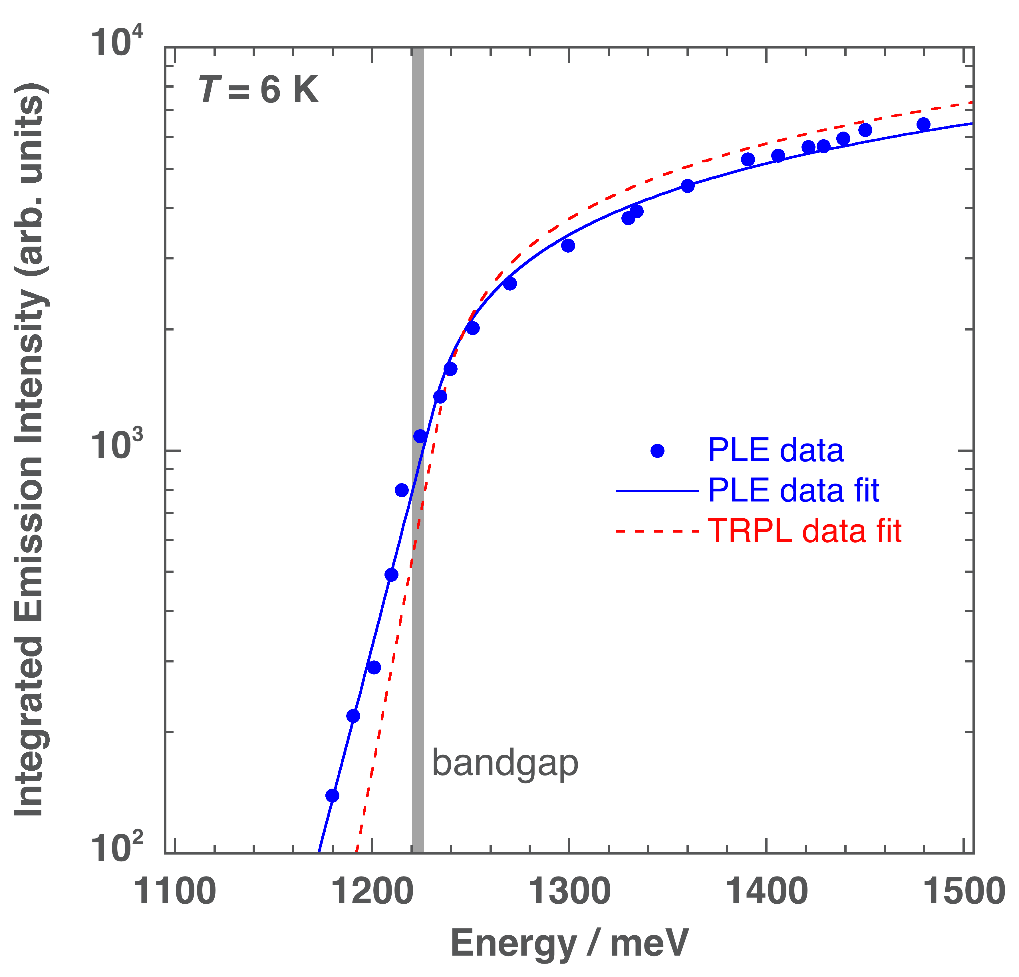
The bandgap is therefore estimated from fitting the PLE data with a square root density of states in the band, above the band gap, typical of direct band gap semiconductors, and a density of band tail states in the gap — related to the localized states — described by a single exponential, as first proposed by Urbach Urbach (1953), which appears to be well adapted to the case at hand.
More precisely, we model the density of states of such a direct band gap semiconductor as:
| (1) |
where is, as usual, the width of the band gap, and is the characteristic energy that scales the extent of the Urbach tail density of localized defect states in the gap; is a global amplitude factor. With the above definition, and its derivative are both continuous functions at the connection energy . This is requested by the smooth behavior of the experimental data around the band gap.
The best least squares fit of the experimental data of figure 1 with this model function is obtained with the values meV, and meV. The grey vertical line in figure 1 covers the energy interval between the values taken from the fits of the PLE data — 1220.4 meV, and TR-PL data — 1226.3 meV (see below).
IV Time-resolved photoluminescence
Another way to estimate the band gap, and the extent of the band tail of localized states just below, is to perform a study of TR-PL spectra Gokmen et al. (2013); Bleuse et al. (2018). These spectra are reported in figure 2 for various time delays after a 1.55 eV, -fs long, pulsed excitation111See Supplemental Material at [URL] for an animated version of a larger subset (144 spectra) of the experimental data and corresponding curve fits, from 0.5 to 200 ns. In figure 2(a), the rise of the TR-PL signal is plotted on a linear scale, which shows a maximum intensity at a 0.90-ns delay: this should correspond to the fast relaxation of the energy of hot carriers within the bands. Then, in figure 2(b), the subsequent signal decay exhibits a red energy shift that increases with time. This reveals the transfer of carriers within a band tail of states below the band gap, from the highest states to the lowest ones, on a much longer time scale — of the order of 100 ns.
These transfers between states of differing energies explain why, in such a case, a decay curve measured at a single photon energy can only accidentally give rise to a single exponential, and would account for only meaningless characteristic transition times.
In the present case, the time-dependent spectra are plotted, on a semi-logarithmic scale, for time delays in a geometric series222Figure 2(b) shows 9 spectra for delays from 1 to 200 ns, geometrically “equidistant”, i.e. for delays separated by a factor , rounded to the time resolution, which is here the time bin width: 50 ps.. In such a scheme, if the PL decay were following a power law dependence on time Mourad et al. (2012); Hages et al. (2017), the intensity maxima between two successive curves should be visually equidistant on this semi-logarithmic plot: it is not the case here, at least for times up to ns, as the larger the time, the closer the spectra look, which evidences that the PL intensity peak decrease is slower than any power law, therefore slower than any exponential. For times larger than ns, the data is not so clear, and a power law behaviour cannot be fully excluded.
From this, we can then infer that the carriers at the origin of the emission in the band tail are not fully independent, since the power law decay inherent to bimolecular recombination Mourad et al. (2012) is absent for delays below 25 ns. It is also worth mentioning here that, at room temperature, such a carrier redistribution in CZTSSe was found to occur over only a much shorter, 1 ns time scale, and on an energy range of only 10 meV Hages et al. (2017).
To get a more quantitative account of our data, we use the following analysis methodology: each of these low-resolution, TR-PL spectra is fitted with a function that is the product of the above density of states (eq. 1) with a Fermi occupation function:
| (2) |
Since the band gap and the Urbach tail extent do not depend on time, the fitting procedure is two-step: the nearly 2000 spectra, from 0.50 ns to 100 ns after the excitation pulse, are fitted333A Levenberg-Marquardt algorithm is used. with the function , keeping the values of and constant, with only 3 parameters varying with time: , , and . The cumulated errors between data and fitted values over these 2000 spectra then represent a global error for the chosen (, ) pair. This is then repeated to find the optimal and values that minimize this global error 444The minimization search goes over the rectangle meV2, where a single global minimum is found at (1226.3; 16.8) meV..

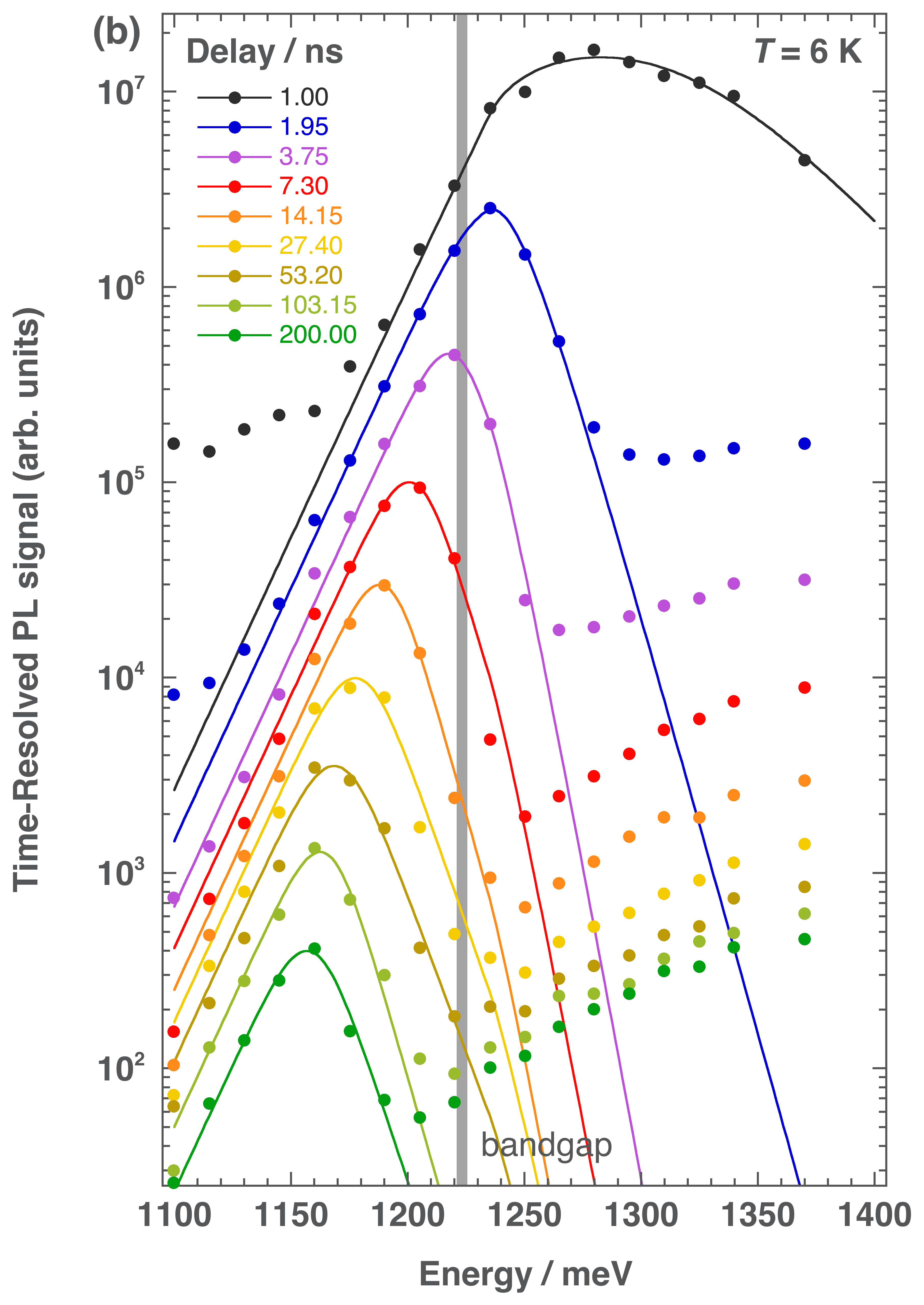
The results of this two-step procedure are given in figure 2, showing the fits (full lines) together with experimental data (points): a bandgap meV, and an Urbach tail characteristic energy meV are precisely found, along with the time variation of the parameters , , and . This determination of and is in good agreement with the one deduced above from the PLE experiments. As in figure 1, the grey vertical line in figure 2 covers the energy interval from 1220.4 to 1226.3 meV.
One must however take note that we do not currently understand the exact nature of the emission that is always observed on the high energy side of the spectra ( eV) ; this emission is also observed in steady-state PL spectra (see figure 3). As it is clearly distinguished from the emission peak, it is not taken into account in our data analysis, .
V Discussion
It is clear from this analysis that the maxima of the TR-PL peak, for very short time delays after the pulse, are at energies larger than (figure 2(a)), and correspond to the recombination of hot carriers, before and along energy relaxation from phonon emission. On the other hand, for delays larger than ns, the maxima of the TR-PL peak occur at energies lower than , and are related to carrier recombination involving localized states in the band tail.
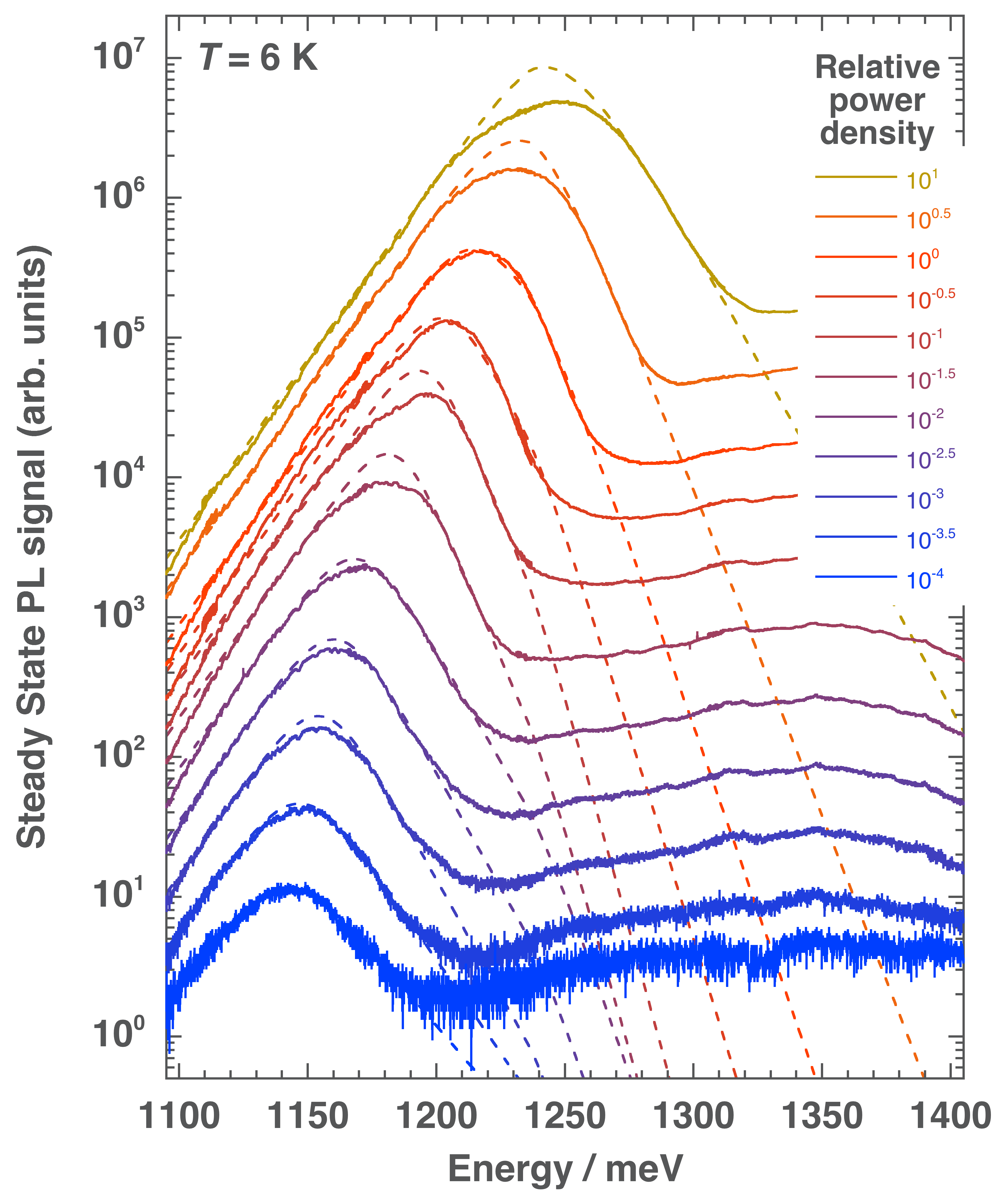
Considering the parameters extracted from the model, the Fermi energy is — for delays larger than 1 ns — a decreasing function of time that closely follows the peak energy maxima, as expected from the characteristics of our model function . This superposition of with the energy variation of the peak maxima is confirmed with steady-state PL spectra as a function of power excitation (see fig.3). There, by varying the power density over five orders of magnitude, the PL maxima are shifted by meV, from 1145 to 1245 meV, as are the values of (see figure 4).
In both sets of experimental data — steady-state PL as a function of power excitation and TR-PL, the emission spectra can be related to the steady-state or instantaneous carrier density. PL peak and Fermi energies, as well as carrier temperatures should therefore correspond when the carrier densities match. This correspondence is attempted in figure 4 where we adjust the excitation power and time scales to show that peak energy and full width at half maximum (FWHM) pairs exhibit similar trends between steady-state and time-resolved PL. This shows that, for delays larger than ns, the carrier populations in TR-PL measurements are probably close to thermal equilibrium.
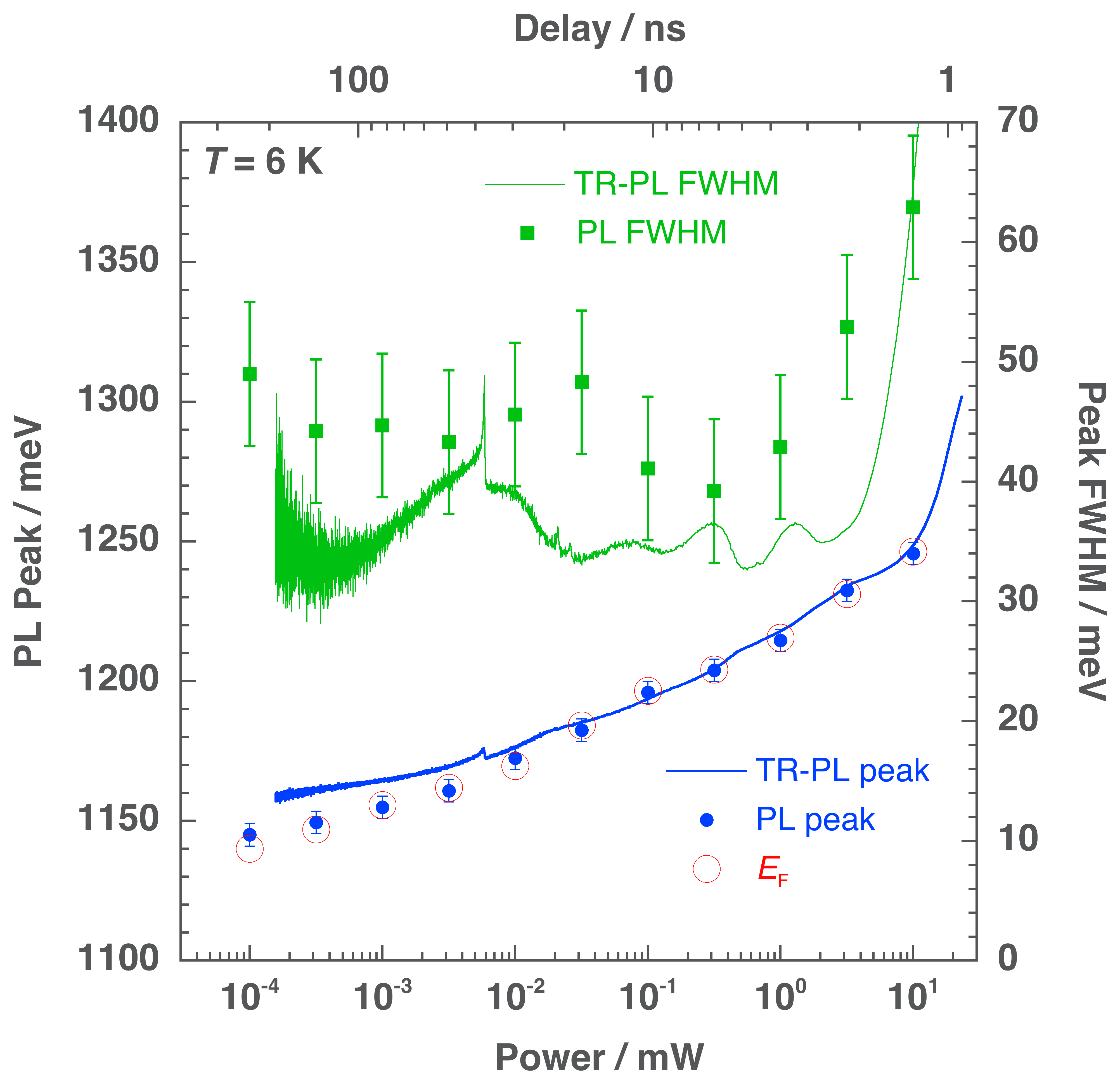
Our second fit parameter, the “temperature” , which is directly related to the peak FWHM, decreases as a function of time and saturates, at delays larger than 5 ns, to a value of meV, which is equivalent to K: this temperature, much larger than the bath one (6 K), shows the limitation of our model to account for weakly-populated discrete defect states in the band tail. Nevertheless, these values of between 1 and 200 ns can be, used to estimate the FWHM (full green line in figure 4), which shows values between 35 and 70 meV, fully accounting for the TR-PL experimental data. These are in very good agreement with the peak FWHM deduced from steady-state PL spectra (green squares), and a factor of 2 smaller than the FWHM usually measured on pure copper kësterites compounds Bleuse et al. (2018); Timmo et al. (2017), which lie between 70 and 110 meV, even for the most ordered CZTS monocrystalline samples.
VI Conclusion
This work reports on a precise determination of the band gap of monocrystalline Ag2ZnSnSe4 at low temperature. Both photoluminescence excitation and time-resolved photoluminescence lead to a value of at 6 K equal to meV. It is worth noting that such values are much lower than the ones reported at room temperature for polycristalline thin films: figuring diffuse reflectance data in a Tauc plot, W. Gong et al Gong et al. (2015) obtained a value of eV, whereas Gershon et al. Gershon et al. (2016b) deduced a value of 1.35 eV from External Quantum Efficiency data, in agreement with their room-temperature PL emission maximum. Variations of the gap values can however be strongly dependent on the selenization temperature, i.e. Se content, as pointed out by Jiang et al. Jiang et al. (2019) who reported band gap values between 1.33 eV and 1.59 eV. Our results nevertheless indicate that the usual behavior of semiconductor band gap — a decrease with temperature because of electron-phonon coupling, does not hold here: further studies as a function of temperature are under way to elucidate this unexpected behavior.
This work also presents a quantitative methodology to precisely deduce the band gap and the characteristic energy for the extent of the tail of localized states, from the PLE and TR-PL data. Such an approach is different from the one usually used, namely measuring the energy shift between the PL emission and the absorption PLE threshold (the Stokes shift). The advantage of the present method is that no arbitrary choice of the low power excitation has to be done to select the PL emission spectrum and its peak energy (see figure 4).
Finally, with this systematic optical spectroscopy study and the above analysis methodology, the characteristic energy of the band tail in this new Ag2ZnSnSe4 material is found to be meV, which leads to a photoluminescence FWHM that is half those usually reported for even the most-ordered Cu-based kësterites compounds.
Acknowledgements.
This research was supported by the french ANR program “Carnot Energies du Futur”, under the project name CAZTS.References
- Urbach (1953) F. Urbach, Physical Review 92, 1324 (1953).
- Moser and Urbach (1956) F. Moser and F. Urbach, Physical Review 102, 1519 (1956).
- Bhattacharyya et al. (2018) B. Bhattacharyya, K. Gahlot, R. Viswanatha, and A. Pandey, The Journal of Physical Chemistry Letters 9, 635 (2018), pMID: 29337575, https://doi.org/10.1021/acs.jpclett.7b03087 .
- Green et al. (2019) M. A. Green, Y. Hishikawa, E. D. Dunlop, D. H. Levi, J. Hohl-Ebinger, M. Yoshita, and A. W. Y. Ho-Baillie, Progress in Photovoltaics 27, 3 (2019).
- Wang et al. (2014) W. Wang, M. T. Winkler, O. Gunawan, T. Gokmen, T. K. Todorov, Y. Zhu, and D. B. Mitzi, Advanced Energy Materials 4 (2014), 10.1002/aenm.201301465.
- Gokmen et al. (2013) T. Gokmen, O. Gunawan, T. K. Todorov, and D. B. Mitzi, Applied Physics Letters 103 (2013), 10.1063/1.4820250.
- Chen et al. (2013) S. Chen, A. Walsh, X.-G. Gong, and S.-H. Wei, Advanced Materials 25, 1522 (2013).
- Chen et al. (2010) S. Chen, J.-H. Yang, X. G. Gong, A. Walsh, and S.-H. Wei, Physical Review B 81 (2010), 10.1103/PhysRevB.81.245204.
- Chen et al. (2012) S. Chen, L.-W. Wang, A. Walsh, X. G. Gong, and S.-H. Wei, Applied Physics Letters 101 (2012), 10.1063/1.4768215.
- Romero et al. (2011) M. J. Romero, H. Du, G. Teeter, Y. Yan, and M. M. Al-Jassim, Physical Review B 84 (2011), 10.1103/PhysRevB.84.165324.
- Rey et al. (2018) G. Rey, G. Larramona, S. Bourdais, C. Chone, B. Delatouche, A. Jacob, G. Dennler, and S. Siebentritt, Solar Energy Materials and Solar Cells 179, 142 (2018).
- Tanaka et al. (2006) K. Tanaka, Y. Miyamoto, H. Uchiki, K. Nakazawa, and H. Araki, Physica Status Solidi A-Applications and Materials Science 203, 2891 (2006).
- Leitao et al. (2011) J. P. Leitao, N. M. Santos, P. A. Fernandes, P. M. P. Salome, A. F. da Cunha, J. C. Gonzalez, G. M. Ribeiro, and F. M. Matinaga, Physical Review B 84 (2011), 10.1103/PhysRevB.84.024120.
- Lin et al. (2015) X. Lin, A. Ennaoui, S. Levcenko, T. Dittrich, J. Kavalakkatt, S. Kretzschmar, T. Unold, and M. C. Lux-Steiner, Applied Physics Letters 106 (2015), 10.1063/1.4905311.
- Oueslati et al. (2015) S. Oueslati, G. Brammertz, M. Buffiere, C. Koeble, T. Oualid, M. Meuris, and J. Poortmans, Solar Energy Materials and Solar Cells 134, 340 (2015).
- Sendler et al. (2016) J. Sendler, M. Thevenin, F. Werner, A. Redinger, S. Li, C. Hagglund, C. Platzer-Bjorkman, and S. Siebentritt, Journal of Applied Physics 120 (2016), 10.1063/1.4962630.
- Lang et al. (2017) M. Lang, C. Zimmermann, C. Kraemmer, T. Renz, C. Huber, H. Kalt, and M. Hetterich, Physical Review B 95 (2017), 10.1103/PhysRevB.95.155202.
- Grossberg et al. (2012) M. Grossberg, J. Krustok, J. Raudoja, and T. Raadik, Applied Physics Letters 101 (2012), 10.1063/1.4750249.
- Grossberg et al. (2014) M. Grossberg, T. Raadik, J. Raudoja, and J. Krustok, Current Applied Physics 14, 447 (2014).
- Siebentritt et al. (2005) S. Siebentritt, N. Papathanasiou, and M. Lux-Steiner, Physica Status Solidi B-Basic Solid State Physics 242, 2627 (2005).
- Bleuse et al. (2018) J. Bleuse, F. Ducroquet, and H. Mariette, Journal of Electronic Materials 47, 4282 (2018).
- Timmo et al. (2017) K. Timmo, M. Kauk-Kuusik, M. Pilvet, T. Raadik, M. Altosaar, M. Danilson, M. Grossberg, J. Raudoja, and K. Emits, Thin Solid Films 633, 122 (2017), 13th E-MRS Spring Meeting, Lille, France, May 02–06, 2016.
- Nakamura et al. (2011) S. Nakamura, T. Maeda, T. Tabata, and T. Wada (2011) pp. 2771–2774, 26th European Photovoltaic Solar Energy Conference (PV-SEC).
- Yuan et al. (2015) Z.-K. Yuan, S. Chen, H. Xiang, X.-G. Gong, A. Walsh, J.-S. Park, I. Repins, and S.-H. Wei, Advanced Functional Materials 25, 6733 (2015).
- Chagarov et al. (2016) E. Chagarov, K. Sardashti, A. C. Kummel, Y. S. Lee, R. Haight, and T. S. Gershon, Journal of Chemical Physics 144 (2016), 10.1063/1.4943270.
- Cui et al. (2014) H. Cui, X. Liu, F. Liu, X. Hao, N. Song, and C. Yan, Applied Physics Letters 104 (2014), 10.1063/1.4863951.
- Gershon et al. (2016a) T. Gershon, Y. S. Lee, P. Antunez, R. Mankad, S. Singh, D. Bishop, O. Gunawan, M. Hopstaken, and R. Haight, Advanced Energy Materials 6 (2016a), 10.1002/aenm.201502468.
- Hages et al. (2016) C. J. Hages, M. J. Koeper, and R. Agrawal, Solar Energy Materials and Solar Cells 145, 342 (2016).
- Curé et al. (2017) Y. Curé, S. Pouget, V. Reita, and H. Boukari, Scripta Materialia 130, 200 (2017).
- Klingshirn (2012) C. F. Klingshirn, “Experimental methods,” in Semiconductor Optics (Springer, Berlin, Heidelberg, 2012) Chap. 25, p. 738.
- Note (1) See Supplemental Material at [URL] for an animated version of a larger subset (144 spectra) of the experimental data and corresponding curve fits, from 0.5 to 200 ns.
- Note (2) Figure 2(b) shows 9 spectra for delays from 1 to 200 ns, geometrically “equidistant”, i.e. for delays separated by a factor , rounded to the time resolution, which is here the time bin width: 50 ps.
- Mourad et al. (2012) D. Mourad, J.-P. Richters, L. Gérard, R. André, J. Bleuse, and H. Mariette, Physical Review B 86 (2012), 10.1103/PhysRevB.86.195308.
- Hages et al. (2017) C. J. Hages, A. Redinger, S. Levcenko, H. Hempel, M. J. Koeper, R. Agrawal, D. Greiner, C. A. Kaufmann, and T. Unold, Advanced Energy Materials 7 (2017), 10.1002/aenm.201700167.
- Note (3) A Levenberg-Marquardt algorithm is used.
- Note (4) The minimization search goes over the rectangle meV2, where a single global minimum is found at (1226.3; 16.8) meV.
- Gong et al. (2015) W. Gong, T. Tabata, K. Takei, M. Morihama, T. Maeda, and T. Wada, Physica Status Solidi C: Current Topics in Solid State Physics 12, 700 (2015), 19th International Conference on Ternary and Multinary Compounds (ICTMC), Niigata, Japan, Sep 01–05, 2014.
- Gershon et al. (2016b) T. Gershon, K. Sardashti, O. Gunawan, R. Mankad, S. Singh, Y. S. Lee, J. A. Ott, A. Kummel, and R. Haight, Advanced Energy Materials 6 (2016b), 10.1002/aenm.201601182.
- Jiang et al. (2019) Y. Jiang, B. Yao, J. Jia, Z. Ding, R. Deng, D. Liu, Y. Sui, H. Wang, and Y. Li, Journal of Applied Physics 125 (2019), 10.1063/1.5055895.